©
Semiconductor Components Industries, LLC, 2003
May, 2003 - Rev. 4
1
Publication Order Number:
NCP803/D
NCP803
Very Low Supply Current
3-Pin Microprocessor
Reset Monitor
The NCP803 is a cost-effective system supervisor circuit designed
to monitor V
CC
in digital systems and provide a reset signal to the host
processor when necessary. No external components are required.
The reset output is driven active within 10
µ
sec of V
CC
falling
through the reset voltage threshold. Reset is maintained active for a
minimum of 140 msec after V
CC
rises above the reset threshold. The
NCP803 has an open drain active-low RESET output. The output of
the NCP803 is guaranteed valid down to V
CC
= 1.0 V and is available
in a SOT-23 package.
The NCP803 is optimized to reject fast transient glitches on the V
CC
line. Low supply current of 1.0
µ
A (V
CC
= 3.2 V) make this device
suitable for battery powered applications.
Features
∑
Precision V
CC
Monitor for 2.5 V, 3.0 V, 3.3 V, and 5.0 V Supplies
∑
Precision Monitoring Voltages from 1.6 V to 4.9 V Available
in 100 mV Steps
∑
140 msec Guaranteed Minimum RESET Output Duration
∑
RESET Output Guaranteed to V
CC
= 1.0 V
∑
Low 1.0
µ
A Supply Current
∑
V
CC
Transient Immunity
∑
Small SOT-23 Package
∑
No External Components
∑
Wide Operating Temperature: -40
∞
C to 105
∞
C
Typical Applications
∑
Computers
∑
Embedded Systems
∑
Battery Powered Equipment
∑
Critical
µ
P Power Supply Monitoring
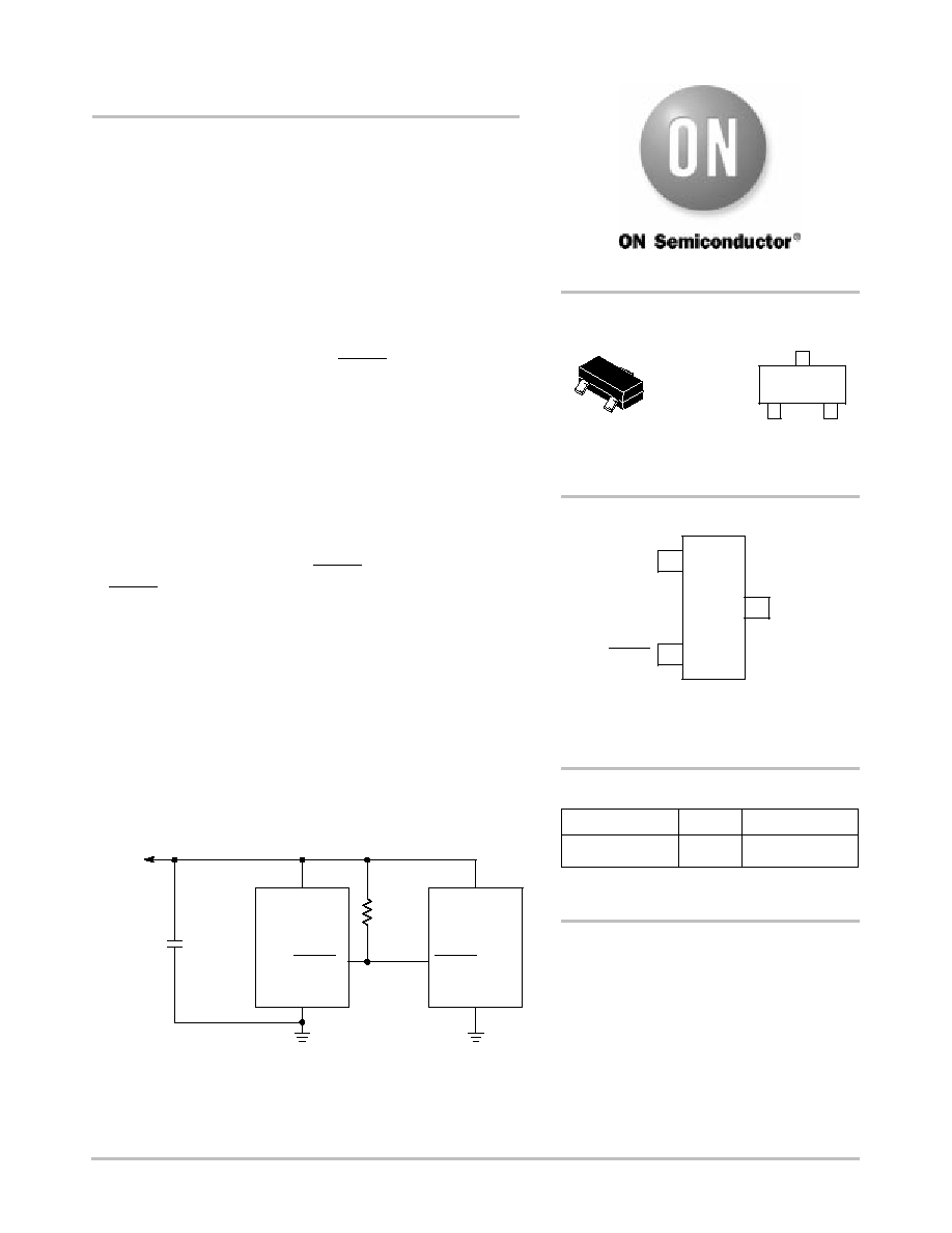
V
CC
V
CC
V
CC
RESET
RESET
NCP803
GND
GND
Figure 1. Typical Application Diagram
µ
P
0
0
R
pull- up
C = 100 nF
SOT-23
(TO-236)
CASE 318
Device
Package
Shipping
ORDERING INFORMATION
NCP803SNxxxT1
SOT-23
3000/Tape & Reel
PIN CONFIGURATION
3
1
2
V
CC
GND
RESET
SOT-23*
NOTE: *SOT-23 is equivalent to JEDEC (TO-236)
(Top View)
See general marking information in the device marking
section on page 6 of this data sheet.
DEVICE MARKING INFORMATION
xxx = Specific Device Code
M = Monthly Date Code
MARKING
DIAGRAM
3
2
1
xxxM
2
1
3
NOTE: The "xxx" denotes a suffix for V
cc
voltage threshold
options - see page 6 for more details.
http://onsemi.com
NCP803
http://onsemi.com
2
PIN DESCRIPTION
Pin No.
Symbol
Description
¡¡¡¡
¡¡¡¡
1
¡¡¡¡¡¡¡
¡¡¡¡¡¡¡
GND
¡¡¡¡¡¡¡¡¡¡¡¡¡¡¡¡¡¡¡¡¡¡¡¡
¡¡¡¡¡¡¡¡¡¡¡¡¡¡¡¡¡¡¡¡¡¡¡¡
Ground
¡¡¡¡
¡
¡¡
¡
¡¡¡¡
2
¡¡¡¡¡¡¡
¡
¡¡¡¡¡
¡
¡¡¡¡¡¡¡
RESET
¡¡¡¡¡¡¡¡¡¡¡¡¡¡¡¡¡¡¡¡¡¡¡¡
¡
¡¡¡¡¡¡¡¡¡¡¡¡¡¡¡¡¡¡¡¡¡¡
¡
¡¡¡¡¡¡¡¡¡¡¡¡¡¡¡¡¡¡¡¡¡¡¡¡
RESET output remains low while V
CC
is below the reset voltage threshold, and for 240 msec (typ.)
after V
CC
rises above reset threshold.
¡¡¡¡
¡¡¡¡
3
¡¡¡¡¡¡¡
¡¡¡¡¡¡¡
V
CC
¡¡¡¡¡¡¡¡¡¡¡¡¡¡¡¡¡¡¡¡¡¡¡¡
¡¡¡¡¡¡¡¡¡¡¡¡¡¡¡¡¡¡¡¡¡¡¡¡
Supply Voltage: C = 100 nF is recommended as a bypass capacitor between V
CC
and GND.
ABSOLUTE MAXIMUM RATINGS*
(Note 1)
Rating
Symbol
Value
Unit
Supply Voltage (V
CC
to GND)
V
CC
6.0
V
RESET
-0.3 to (V
CC
+ 0.3)
V
Input Current, V
CC
20
mA
Output Current, RESET
20
mA
dV/dt (V
CC
)
100
V/
µ
sec
Thermal Resistance, Junction to Air
R
q
JA
491
∞
C/W
Operating Temperature Range
T
A
-40 to +105
∞
C
Storage Temperature Range
T
stg
-65 to +150
∞
C
Lead Temperature (Soldering, 10 Seconds)
T
sol
+260
∞
C
Latch-up performance:
Negative
I
Latch- up
150
mA
*Maximum Ratings are those values beyond which damage to the device may occur.
1. This device series contains ESD protection and exceeds the following tests:
Human Body Model 4000 V per MIL-STD-883, Method 3015.
Machine Model Method 400 V.
2. The maximum package power dissipation limit must not be exceeded.
PD
+
TJ(max)
*
TA
R
q
JA
with T
J(max)
= 150
∞
C

NCP803
http://onsemi.com
3
ELECTRICAL CHARACTERISTICS
T
A
= -40
∞
C to +105
∞
C unless otherwise noted. Typical values are at T
A
= +25
∞
C. (Note 3)
Characteristic
Symbol
Min
Typ
Max
Unit
V
CC
Range
T
A
= 0
∞
C to +70
∞
C
T
A
= -40
∞
C to +105
∞
C
1.0
1.2
-
-
5.5
5.5
V
Supply Current
V
CC
= 3.3 V
T
A
= -40
∞
C to +85
∞
C
T
A
= 85
∞
C to +105
∞
C
V
CC
= 5.5 V
T
A
= -40
∞
C to +85
∞
C
T
A
= 85
∞
C to +105
∞
C
I
CC
-
-
-
-
0.5
-
0.8
-
1.2
2.0
1.8
2.5
µ
A
Reset Threshold (Note 4)
NCP803SN463
T
A
= +25
∞
C
T
A
= -40
∞
C to +85
∞
C
T
A
= +85
∞
C to +105
∞
C
NCP803SN438
T
A
= +25
∞
C
T
A
= -40
∞
C to +85
∞
C
T
A
= +85
∞
C to +105
∞
C
NCP803SN308
T
A
= +25
∞
C
T
A
= -40
∞
C to +85
∞
C
T
A
= +85
∞
C to +105
∞
C
NCP803SN293
T
A
= +25
∞
C
T
A
= -40
∞
C to +85
∞
C
T
A
= +85
∞
C to +105
∞
C
NCP803SN263
T
A
= +25
∞
C
T
A
= -40
∞
C to +85
∞
C
T
A
= +85
∞
C to +105
∞
C
NCP803SN232
T
A
= +25
∞
C
T
A
= -40
∞
C to +85
∞
C
T
A
= +85
∞
C to +105
∞
C
NCP803SN160
T
A
= +25
∞
C
T
A
= -40
∞
C to +85
∞
C
T
A
= +85
∞
C to +105
∞
C
V
TH
4.56
4.51
4.39
4.31
4.27
4.16
3.04
3.00
2.92
2.89
2.85
2.78
2.59
2.55
2.50
2.29
2.26
2.20
1.58
1.56
1.52
4.63
-
-
4.38
-
-
3.08
-
-
2.93
-
-
2.63
-
-
2.32
-
-
1.60
-
-
4.70
4.75
4.87
4.45
4.49
4.60
3.11
3.15
3.23
2.96
3.00
3.08
2.66
2.70
2.76
2.35
2.38
2.44
1.62
1.64
1.68
V
Reset Temperature Coefficient
-
30
-
ppm/
∞
C
V
CC
to Reset Delay V
CC
= V
TH
to (V
TH
- 100 mV)
-
10
-
µ
sec
Reset Active Timeout Period
140
240
460
msec
RESET Output Voltage Low
V
CC
= V
TH
- 0.2 V
1.6 V
v
V
TH
v
2.0 V, I
SINK
= 0.5 mA
2.1 V
v
V
TH
v
4.0 V, I
SINK
= 1.2 mA
4.1 V
v
V
TH
v
4.9 V, I
SINK
= 3.2 mA
V
OL
-
-
0.3
V
RESET Leakage Current
V
CC
u
V
TH
, RESET De-asserted
I
LEAK
-
-
1
µ
A
3. Production testing done at T
A
= 25
∞
C, over temperature limits guaranteed by design.
4. Contact your ON Semiconductor sales representative for other threshold voltage options.
NCP803
http://onsemi.com
4
APPLICATIONS INFORMATION
V
CC
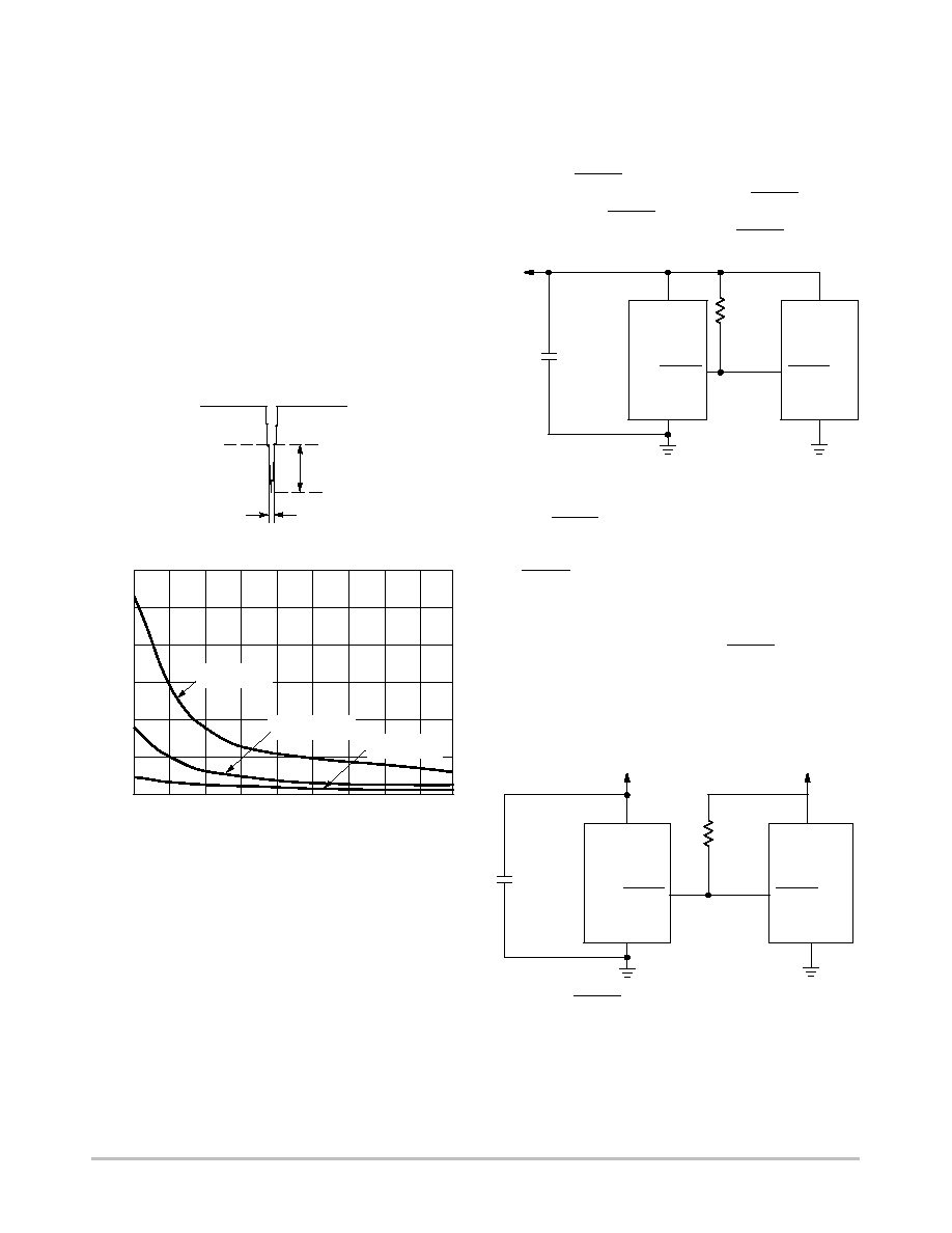
Transient Rejection
The NCP803 provides accurate V
CC
monitoring and reset
timing during power-up, power-down, and brownout/sag
conditions, and rejects negative-going transients (glitches)
on the power supply line. Figure 2 shows the maximum
transient duration vs. maximum negative excursion
(overdrive) for glitch rejection. Any combination of
duration and overdrive which lies under the curve will not
generate a reset signal. Combinations above the curve are
detected as a brownout or power-down. Typically, transient
that goes 100 mV below the reset threshold and lasts 5
µ
s or
less will not cause a reset pulse. Transient immunity can be
improved by adding a capacitor in close proximity to the V
CC
pin.
Figure 2. Maximum Transient Duration vs. Overdrive
for Glitch Rejection at 25
∞
C
Duration
V
TH
Overdrive
V
CC
10
250
200
40
30
MAXIMUM
TRANSIENT DURA
TION (
µ
s) I
50
300
RESET COMPARATOR OVERDRIVE (mV)
0
60
150
100
20
50
70
80
90 100
V
TH
= 3.08 V
V
TH
= 1.6 V
V
TH
= 4.9 V
Processors With Bidirectional I/O Pins
Some
µ
P's (such as Motorola 68HC11) have
bi-directional reset pins which interface easily with the
Open Drain RESET output of the NCP803. As shown in
Figure 3, one can connect directly to the RESET output of
the NCP803 to the RESET pin of the
µ
P. The pull-up resistor
avoids an undetermined voltage of the RESET pin.
Figure 3. Interfacing to Bidirectional Reset I/O
V
CC
V
CC
V
CC
RESET
RESET
NCP803
GND
GND
µ
P
0
0
R
pull- up
C = 100 nF
NCP803 RESET Output Allows Use With Two Power
Supplies
In numerous applications the pull-up resistor placed on
the RESET output is connected to the supply voltage
monitored by the IC. Nevertheless, a different supply
voltage can also power this output and so level-shift from
the monitored supply to reset the
µ
P. However, if the
NCP803's supply goes below 1 V, the RESET output ability
to sink current will decrease and the result is a high state on
the pin even though the supply's IC is under the threshold
level. This occurs at a V
CC
level that depends on the R
pull- up
value and the voltage to which it is connected.
Figure 4. RESET Output with Two Power Supplies
V
CC
V
CC
RESET
RESET
NCP803
GND
GND
µ
P
0
0
R
pull- up
C = 100 nF
+3.3 V
+5.0 V

NCP803
http://onsemi.com
5
TYPICAL CHARACTERISTICS
1.4
1.2
1.0
0.8
0.6
0.4
0.2
0
0.5
1.5
2.5
3.5
4.5
5.5
-40
-20
0
20
40
60
80
0.993
SUPPLY VOLTAGE (V)
TEMPERATURE (
∞
C)
105
∞
C
Figure 5. Supply Current vs. Supply Voltage
1.4
1.2
1.0
0.8
0.6
0.4
0.2
0
SUPPLY VOLTAGE (V)
SUPPL
Y CURRENT (
m
A)
SUPPL
Y CURRENT (
m
A)
1.6
1.8
85
∞
C
25
∞
C
-40
∞
C
0
∞
C
0.5
1.5
2.5
3.5
4.5
5.5
105
∞
C
85
∞
C
25
∞
C
-40
∞
C
0
∞
C
V
TH
= 3.08 V
1.4
1.2
1.0
0.8
0.6
0.4
0.2
0
0.5
1.5
2.5
3.5
4.5
5.5
SUPPLY VOLTAGE (V)
105
∞
C
1.6
85
∞
C
25
∞
C
-40
∞
C
0
∞
C
SUPPL
Y CURRENT (
m
A)
V
TH
= 4.90 V
NORMALIZED V
TH
VOL
T
AGE
0.994
0.995
0.996
0.997
0.998
0.999
1.000
1.001
100
120
V
TH
= 3.08 V
V
TH
= 4.90 V
-40
-20
0
20
40
60
80
200
TEMPERATURE (
∞
C)
POWER-UP RESET TIMEOUT (mS)
210
220
230
240
250
260
270
280
100
120
V
TH
= 1.60 V
V
TH
= 3.08 V
V
TH
= 4.90 V
V
TH
= 1.60 V
V
TH
= 1.60 V
-40
-20
0
20
40
60
80
0
TEMPERATURE (
∞
C)
POWER-DOWN RESET TIMEOUT (
m
S)
50
100
150
200
250
300
350
100
V
TH
= 1.60 V
V
TH
= 3.08 V
V
TH
= 4.90 V
Figure 6. Supply Current vs. Supply Voltage
Figure 7. Supply Current vs. Supply Voltage
Figure 8. Normalized Reset Threshold Voltage
vs. Temperature
Figure 9. Power-up Reset Timeout vs. Temperature
Figure 10. Power-down Reset Timeout vs.
Temperature (Overdrive = 20 mV)
NCP803
http://onsemi.com
6
TAPING FORM
PIN 1
USER DIRECTION OF FEED
Component Taping Orientation for 3L SOT-23 (JEDEC-236) Devices
Standard Reel Component Orientation
(Mark Right Side Up)
DEVICE
MARKING
SOT-23
Package
Carrier Width (W)
Pitch (P)
Part Per Full Reel
Reel Size
8 mm
4 mm
3000
7 inches
Tape & Reel Specifications Table
MARKING AND THRESHOLD INFORMATION
ON Semicond ctor Part #
V
*
Marking (Note 5)
ON Semiconductor Part #
V
TH
*
Marking (Note 5)
NCP803SN160T1
1.60
SCQM
NCP803SN232T1
2.32
SQRM
NCP803SN263T1
2.63
SQCM
NCP803SN293T1
2.93
SQDM
NCP803SN308T1
3.08
SQEM
NCP803SN438T1
4.38
SQFM
NCP803SN463T1
4.63
SQGM
*Contact your ON Semiconductor sales representative for other threshold voltage options.
5. M = Monthly Date Code

NCP803
http://onsemi.com
7
PACKAGE DIMENSIONS
SOT-23
PLASTIC PACKAGE (TO-236)
CASE 318-08
ISSUE AH
D
J
K
L
A
C
B S
H
G
V
3
1
2
DIM
A
MIN
MAX
MIN
MAX
MILLIMETERS
0.1102 0.1197
2.80
3.04
INCHES
B 0.0472 0.0551
1.20
1.40
C 0.0350 0.0440
0.89
1.11
D 0.0150 0.0200
0.37
0.50
G 0.0701 0.0807
1.78
2.04
H 0.0005 0.0040
0.013
0.100
J 0.0034 0.0070
0.085
0.177
K 0.0140 0.0285
0.35
0.69
L 0.0350 0.0401
0.89
1.02
S 0.0830 0.1039
2.10
2.64
V 0.0177 0.0236
0.45
0.60
NOTES:
1. DIMENSIONING AND TOLERANCING PER ANSI
Y14.5M, 1982.
2. CONTROLLING DIMENSION: INCH.
3. MAXIMUM LEAD THICKNESS INCLUDES LEAD
FINISH THICKNESS. MINIMUM LEAD THICKNESS
IS THE MINIMUM THICKNESS OF BASE
MATERIAL.
4. 318-03 AND -07 OBSOLETE, NEW STANDARD
318-08.

NCP803
http://onsemi.com
8
ON Semiconductor and are registered trademarks of Semiconductor Components Industries, LLC (SCILLC). SCILLC reserves the right to make
changes without further notice to any products herein. SCILLC makes no warranty, representation or guarantee regarding the suitability of its products for any
particular purpose, nor does SCILLC assume any liability arising out of the application or use of any product or circuit, and specifically disclaims any and all
liability, including without limitation special, consequential or incidental damages. "Typical" parameters which may be provided in SCILLC data sheets and/or
specifications can and do vary in different applications and actual performance may vary over time. All operating parameters, including "Typicals" must be
validated for each customer application by customer's technical experts. SCILLC does not convey any license under its patent rights nor the rights of others.
SCILLC products are not designed, intended, or authorized for use as components in systems intended for surgical implant into the body, or other applications
intended to support or sustain life, or for any other application in which the failure of the SCILLC product could create a situation where personal injury or death
may occur. Should Buyer purchase or use SCILLC products for any such unintended or unauthorized application, Buyer shall indemnify and hold SCILLC
and its officers, employees, subsidiaries, affiliates, and distributors harmless against all claims, costs, damages, and expenses, and reasonable attorney fees
arising out of, directly or indirectly, any claim of personal injury or death associated with such unintended or unauthorized use, even if such claim alleges that
SCILLC was negligent regarding the design or manufacture of the part. SCILLC is an Equal Opportunity/Affirmative Action Employer.
PUBLICATION ORDERING INFORMATION
JAPAN: ON Semiconductor, Japan Customer Focus Center
2-9-1 Kamimeguro, Meguro-ku, Tokyo, Japan 153-0051
Phone: 81-3-5773-3850
ON Semiconductor Website: http://onsemi.com
For additional information, please contact your local
Sales Representative.
NCP803/D
SENSEFET is a trademark of Semiconductor Components Industries, LLC.
Literature Fulfillment:
Literature Distribution Center for ON Semiconductor
P.O. Box 5163, Denver, Colorado 80217 USA
Phone: 303-675-2175 or 800-344-3860 Toll Free USA/Canada
Fax: 303-675-2176 or 800-344-3867 Toll Free USA/Canada
Email: ONlit@hibbertco.com
N. American Technical Support: 800-282-9855 Toll Free USA/Canada