 | –≠–ª–µ–∫—Ç—Ä–æ–Ω–Ω—ã–π –∫–æ–º–ø–æ–Ω–µ–Ω—Ç: NCS2001 | –°–∫–∞—á–∞—Ç—å:  PDF PDF  ZIP ZIP |
©
Semiconductor Components Industries, LLC, 2002
November, 2002 - Rev. 8
1
Publication Order Number:
NCS2001/D
NCS2001
0.9 V, Rail-to-Rail, Single
Operational Amplifier
The NCS2001 is an industry first sub-one volt operational amplifier
that features a rail-to-rail common mode input voltage range, along
with rail-to-rail output drive capability. This amplifier is guaranteed
to be fully operational down to 0.9 V, providing an ideal solution for
powering applications from a single cell Nickel Cadmium (NiCd) or
Nickel Metal Hydride (NiMH) battery. Additional features include no
output phase reversal with overdriven inputs, trimmed input offset
voltage of 0.5 mV, extremely low input bias current of 40 pA, and a
unity gain bandwidth of 1.4 MHz at 5.0 V. The tiny NCS2001 is the
ideal solution for small portable electronic applications and is
available in the space saving SOT23-5 and SC70-5 packages with
two industry standard pinouts.
Features
∑
0.9 V Guaranteed Operation
∑
Rail-to-Rail Common Mode Input Voltage Range
∑
Rail-to-Rail Output Drive Capability
∑
No Output Phase Reversal for Over- Driven Input Signals
∑
0.5 mV Trimmed Input Offset
∑
10 pA Input Bias Current
∑
1.4 MHz Unity Gain Bandwidth at
"2.5 V, 1.1 MHz at "0.5 V
∑
Tiny SC70-5 and SOT23-5 Packages
Typical Applications
∑
Single Cell NiCd/NiMH Battery Powered Applications
∑
Cellular Telephones
∑
Pagers
∑
Personal Digital Assistants
∑
Electronic Games
∑
Digital Cameras
∑
Camcorders
∑
Hand Held Instruments
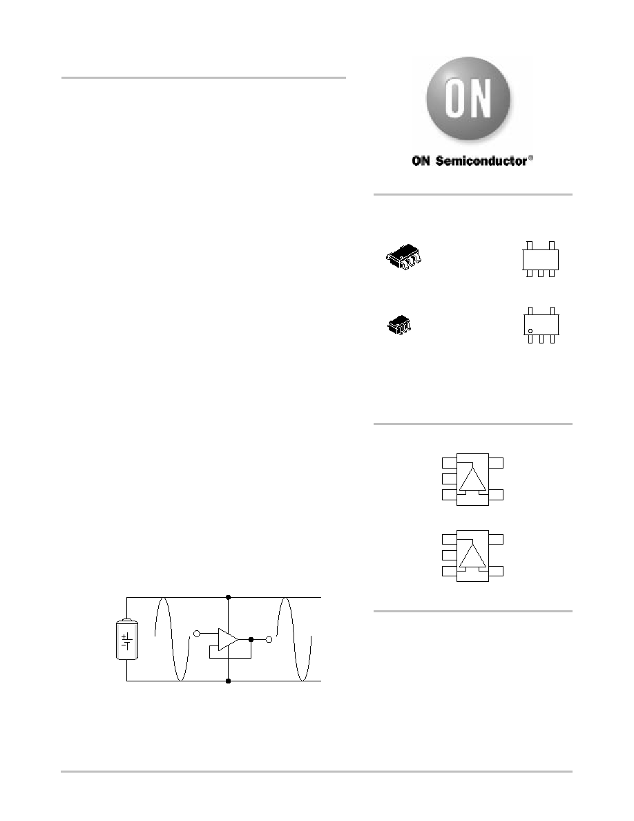
Figure 1. Typical Application
This device contains 63 active transistors.
-
+
0.8 V
to
7.0 V
Rail to Rail Input
Rail to Rail Output
ORDERING INFORMATION
SOT23-5
(TSOP-5/SC59-5)
SN SUFFIX
CASE 483
PIN CONNECTIONS
1
V
OUT
V
CC
Non-Inverting
Input
2
3
5
4
V
EE
Inverting
Input
Style 1 Pinout (SN1T1, SQ1T1)
+ -
1
V
OUT
V
EE
Non-Inverting
Input
2
3
5
4
V
CC
Inverting
Input
Style 2 Pinout (SN2T1, SQ2T1)
+ -
MARKING
DIAGRAMS
1
5
AAxYW
x = G for SN1
H for SN2
I for SQ1
J for SQ2
1 2
3
4
5
SC70-5
(SC-88A /SOT-353)
SQ SUFFIX
CASE 419A
AAx
M
1
5
1
5
Y = Year
W = Work Week
M = Date Code
See detailed ordering and shipping information in the
dimensions section on page 15 of this data sheet.
http://onsemi.com

NCS2001
http://onsemi.com
2
MAXIMUM RATINGS
Rating
Symbol
Value
Unit
Supply Voltage (V
CC
to V
EE
)
V
S
7.0
V
Input Differential Voltage Range (Note 1)
V
IDR
V
EE
-300 mV to
7.0 V
V
Input Common Mode Voltage Range (Note 1)
V
ICR
V
EE
-300 mV to
7.0 V
V
Output Short Circuit Duration (Note 2)
t
Sc
Indefinite
sec
Junction Temperature
T
J
150
∞
C
Power Dissipation and Thermal Characteristics
SOT23-5 Package
Thermal Resistance, Junction to Air
Power Dissipation @ T
A
= 70
∞
C
SC70-5 Package
Thermal Resistance, Junction to Air
Power Dissipation @ T
A
= 70
∞
C
R
q
JA
P
D
R
q
JA
P
D
235
340
280
286
∞
C/W
mW
∞
C/W
mW
Storage Temperature Range
T
stg
-65 to 150
∞
C
ESD Protection at any Pin Human Body Model (Note 3)
V
ESD
2000
V
1. Either or both inputs should not exceed the range of V
EE
-300 mV to V
EE
+7.0 V.
2. Maximum package power dissipation limits must be observed to ensure that the maximum junction temperature is not exceeded.
T
J
= T
A
+ (P
D
R
q
JA
)
3. ESD data available upon request.
DC ELECTRICAL CHARACTERISTICS
(V
CC
= 2.5 V, V
EE
= -2.5 V, V
CM
= V
O
= 0 V, R
L
to Gnd, T
A
= 25
∞
C unless otherwise noted.)
Characteristics
Symbol
Min
Typ
Max
Unit
Input Offset Voltage
V
CC
= 0.45 V, V
EE
= -0.45 V
T
A
= 25
∞
C
T
A
= 0
∞
C to 70
∞
C
T
A
= -40
∞
C to 105
∞
C
V
CC
= 1.5 V, V
EE
= -1.5 V
T
A
= 25
∞
C
T
A
= 0
∞
C to 70
∞
C
T
A
= -40
∞
C to 105
∞
C
V
CC
= 2.5 V, V
EE
= -2.5 V
T
A
= 25
∞
C
T
A
= 0
∞
C to 70
∞
C
T
A
= -40
∞
C to 105
∞
C
V
IO
-6.0
-8.5
-9.5
-6.0
-7.0
-7.5
-6.0
-7.5
-7.5
0.5
-
-
0.5
-
-
0.5
-
-
6.0
8.5
9.5
6.0
7.0
7.5
6.0
7.5
7.5
mV
Input Offset Voltage Temperature Coefficient (R
S
= 50)
T
A
= -40
∞
C to 105
∞
C
D
V
IO
/
D
T
-
8.0
-
m
V/
∞
C
Input Bias Current (V
CC
= 1.0 V to 5.0 V)
I
IB
-
10
-
pA
Input Common Mode Voltage Range
V
ICR
-
V
EE
to V
CC
-
V
Large Signal Voltage Gain
V
CC
= 0.45 V, V
EE
= -0.45 V
R
L
= 10 k
R
L
= 2.0 k
V
CC
= 1.5 V, V
EE
= -1.5 V
R
L
= 10 k
R
L
= 2.0 k
V
CC
= 2.5 V, V
EE
= -2.5 V
R
L
= 10 k
R
L
= 2.0 k
A
VOL
-
-
-
-
20
15
40
20
40
40
40
40
-
-
-
-
-
-
kV/V
NCS2001
http://onsemi.com
3
DC ELECTRICAL CHARACTERISTICS (continued)
(V
CC
= 2.5 V, V
EE
= -2.5 V, V
CM
= V
O
= 0 V, R
L
to Gnd, T
A
= 25
∞
C unless otherwise noted.)
Characteristics
Unit
Max
Typ
Min
Symbol
Output Voltage Swing, High State Output (V
ID
= +0.5 V)
V
CC
= 0.45 V, V
EE
= -0.45 V
T
A
= 25
∞
C
R
L
= 10 k
R
L
= 2.0 k
T
A
= 0
∞
C to 70
∞
C
R
L
= 10 k
R
L
= 2.0 k
T
A
= -40
∞
C to 105
∞
C
R
L
= 10 k
R
L
= 2.0 k
V
CC
= 1.5 V, V
EE
= -1.5 V
T
A
= 25
∞
C
R
L
= 10 k
R
L
= 2.0 k
T
A
= 0
∞
C to 70
∞
C
R
L
= 10 k
R
L
= 2.0 k
T
A
= -40
∞
C to 105
∞
C
R
L
= 10 k
R
L
= 2.0 k
V
CC
= 2.5 V, V
EE
= -2.5 V
T
A
= 25
∞
C
R
L
= 10 k
R
L
= 2.0 k
T
A
= 0
∞
C to 70
∞
C
R
L
= 10 k
R
L
= 2.0 k
T
A
= -40
∞
C to 105
∞
C
R
L
= 10 k
R
L
= 2.0 k
V
OH
0.40
0.35
0.40
0.35
0.40
0.35
1.45
1.40
1.45
1.40
1.45
1.40
2.45
2.40
2.45
2.40
2.45
2.40
0.494
0.466
-
-
-
-
1.498
1.480
-
-
-
-
2.498
2.475
-
-
-
-
-
-
-
-
-
-
-
-
-
-
-
-
-
-
-
-
-
-
V
Output Voltage Swing, Low State Output (V
ID
= -0.5 V)
V
CC
= 0.45 V, V
EE
= -0.45 V
T
A
= 25
∞
C
R
L
= 10 k
R
L
= 2.0 k
T
A
= 0
∞
C to 70
∞
C
R
L
= 10 k
R
L
= 2.0 k
T
A
= -40
∞
C to 105
∞
C
R
L
= 10 k
R
L
= 2.0 k
V
CC
= 1.5 V, V
EE
= -1.5 V
T
A
= 25
∞
C
R
L
= 10 k
R
L
= 2.0 k
T
A
= 0
∞
C to 70
∞
C
R
L
= 10 k
R
L
= 2.0 k
T
A
= -40
∞
C to 105
∞
C
R
L
= 10 k
R
L
= 2.0 k
V
CC
= 2.5 V, V
EE
= -2.5 V
T
A
= 25
∞
C
R
L
= 10 k
R
L
= 2.0 k
T
A
= 0
∞
C to 70
∞
C
R
L
= 10 k
R
L
= 2.0 k
T
A
= -40
∞
C to 105
∞
C
R
L
= 10 k
R
L
= 2.0 k
V
OL
-
-
-
-
-
-
-
-
-
-
-
-
-
-
-
-
-
-
-0.494
-0.480
-
-
-
-
-1.493
-1.480
-
-
-
-
-2.492
-2.479
-
-
-
-
-0.40
-0.35
-0.40
-0.35
-0.40
-0.35
-1.45
-1.40
-1.45
-1.40
-1.45
-1.40
-2.45
-2.40
-2.45
-2.40
-2.45
-2.40
V
NCS2001
http://onsemi.com
4
DC ELECTRICAL CHARACTERISTICS (continued)
(V
CC
= 2.5 V, V
EE
= -2.5 V, V
CM
= V
O
= 0 V, R
L
to Gnd, T
A
= 25
∞
C unless otherwise noted.)
Characteristics
Unit
Max
Typ
Min
Symbol
Common Mode Rejection Ratio (V
in
= 0 to 5.0 V)
CMRR
60
70
-
dB
Power Supply Rejection Ratio (V
CC
= 0.5 V to 2.5 V, V
EE
= -2.5 V)
PSRR
55
65
-
dB
Output Short Circuit Current
V
CC
= 0.45 V, V
EE
= -0.45 V, V
ID
=
"
0.4 V
Source Current High Output State
Sink Current Low Output State
V
CC
= 1.5 V, V
EE
= -1.5 V, V
ID
=
"
0.5 V
Source Current High Output State
Sink Current Low Output State
V
CC
= 2.5 V, V
EE
= -2.5 V, V
ID
=
"
0.5 V
Source Current High Output State
Sink Current Low Output State
I
SC
0.5
-
15
-
40
-
1.2
-3.0
29
-40
76
-96
-
-1.5
-
-20
-
-50
mA
Power Supply Current (Per Amplifier, V
O
= 0 V)
V
CC
= 0.45 V, V
EE
= -0.45 V
T
A
= 25
∞
C
T
A
= 0
∞
C to 70
∞
C
T
A
= -40
∞
C to 105
∞
C
V
CC
= 1.5 V, V
EE
= -1.5 V
T
A
= 25
∞
C
T
A
= 0
∞
C to 70
∞
C
T
A
= -40
∞
C to 105
∞
C
V
CC
= 2.5 V, V
EE
= -2.5 V
T
A
= 25
∞
C
T
A
= 0
∞
C to 70
∞
C
T
A
= -40
∞
C to 105
∞
C
I
D
-
-
-
-
-
-
-
-
-
0.51
-
-
0.72
-
-
0.82
-
-
1.10
1.10
1.10
1.40
1.40
1.40
1.50
1.50
1.50
mA
AC ELECTRICAL CHARACTERISTICS
(V
CC
= 2.5 V, V
EE
= -2.5 V, V
CM
= V
O
= 0 V, R
L
to Gnd, T
A
= 25
∞
C unless otherwise noted.)
Characteristics
Symbol
Min
Typ
Max
Unit
Differential Input Resistance (V
CM
= 0 V)
R
in
-
u
1.0
-
tera
W
Differential Input Capacitance (V
CM
= 0 V)
C
in
-
3.0
-
pF
Equivalent Input Noise Voltage (f = 1.0 kHz)
e
n
-
100
-
nV/
Hz
Gain Bandwidth Product (f = 100 kHz)
V
CC
= 0.45 V, V
EE
= -0.45 V
V
CC
= 1.5 V, V
EE
= -1.5 V
V
CC
= 2.5 V, V
EE
= -2.5 V
GBW
-
-
0.5
1.1
1.3
1.4
-
-
-
MHz
Gain Margin (R
L
= 10 k, C
L
= 5.0 pf)
Am
-
6.5
-
dB
Phase Margin (R
L
= 10 k, C
L
= 5.0 pf)
f
m
-
60
-
Deg
Power Bandwidth (V
O
= 4.0 Vpp, R
L
= 2.0 k, THD = 1.0%, A
V
= 1.0)
BW
P
-
80
-
kHz
Total Harmonic Distortion (V
O
= 4.0 Vpp, R
L
= 2.0 k, A
V
= 1.0)
f = 1.0 kHz
f = 10 kHz
THD
-
-
0.008
0.08
-
-
%
Slew Rate (V
S
=
"
2.5 V, V
O
= -2.0 V to 2.0 V, R
L
= 2.0 k, A
V
= 1.0)
Positive Slope
Negative Slope
SR
1.0
1.0
1.6
1.6
6.0
6.0
V/
m
s
NCS2001
http://onsemi.com
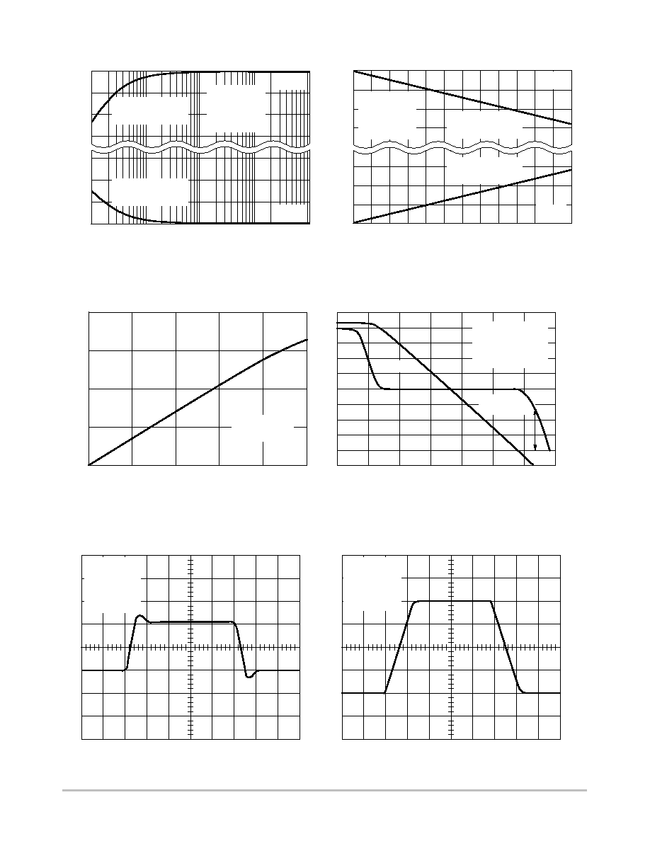
5
1.0
20
80
10 k
60
100 k
1.0 k
100
1.0 M
40
0
10
V
CC
= 2.5 V
V
EE
= -2.5 V
R
L
= 10 k to Gnd
T
A
= 25
∞
C
100
10 M
Phase
Margin = 60
∞
Gain
Phase
0
45
90
135
180
t, time (1.0
m
s/Div)
t, time (500 ns/Div)
V
S
=
±
2.5 V
R
L
= 10 k
C
L
= 10 pf
A
V
= 1.0
T
A
= 25
∞
C
T
A
, Ambient Temperature (
∞
C)
Figure 2. Split Supply Output Saturation vs.
Load Resistance
Figure 3. Split Supply Output Saturation vs.
Load Current
Figure 4. Input Bias Current vs. Temperature
Figure 5. Gain and Phase vs. Frequency
Figure 6. Transient Response
Figure 7. Slew Rate
0
100
1.0 k
10 k
100 k
1.0 M
R
L
, Load Resistance (
W
)
0.2
0.4
0.6
-0.6
-0.4
-0.2
0
V
CC
V
EE
High State Output
Sourcing Current
Low State Output
Sinking Current
V
CC
= 2.5 V
V
EE
= -2.5 V
R
L
to Gnd
T
A
= 25
∞
C
0
0
2.0
8.0
10
12
I
L
, Load Current (mA)
0.1
0.2
0.3
-0.3
-0.2
-0.1
0
V
CC
V
EE
High State Output
Sourcing Current
Low State Output
Sinking Current
V
CC
= 2.5 V
V
EE
= -2.5 V
I
L
to Gnd
T
A
= 25
∞
C
4.0
6.0
V
S
=
±
2.5 V
A
V
= 1.0
R
L
= 10 k
C
L
= 10 pF
T
A
= 25
∞
C
A
VO
L
, Gain (dB)
V
sat
, Output Saturation V
oltage (V)
I
IB
, Input Current (pA)
f, Frequency (Hz)
F
m, Excess Phase (
∞
)
1000
100
1.0
0
0
25
50
75
100
125
10
V
CC
= 2.5 V
V
EE
= -2.5 V
500 mV/div
50 mV/div
V
sat
, Output Saturation V
oltage (V)