©
Semiconductor Components Industries, LLC, 2005
August, 2005 - Rev. 8
1
Publication Order Number:
LM317/D
LM317, NCV317
1.5 A Adjustable Output,
Positive Voltage Regulator
The LM317 is an adjustable 3-terminal positive voltage regulator
capable of supplying in excess of 1.5 A over an output voltage range of
1.2 V to 37 V. This voltage regulator is exceptionally easy to use and
requires only two external resistors to set the output voltage. Further, it
employs internal current limiting, thermal shutdown and safe area
compensation, making it essentially blow-out proof.
The LM317 serves a wide variety of applications including local, on
card regulation. This device can also be used to make a programmable
output regulator, or by connecting a fixed resistor between the
adjustment and output, the LM317 can be used as a precision current
regulator.
Features
∑
Output Current in Excess of 1.5 A
∑
Output Adjustable between 1.2 V and 37 V
∑
Internal Thermal Overload Protection
∑
Internal Short Circuit Current Limiting Constant with Temperature
∑
Output Transistor Safe-Area Compensation
∑
Floating Operation for High Voltage Applications
∑
Available in Surface Mount D
2
PAK-3, and Standard 3-Lead
Transistor Package
∑
Eliminates Stocking many Fixed Voltages
∑
Pb-Free Packages are Available
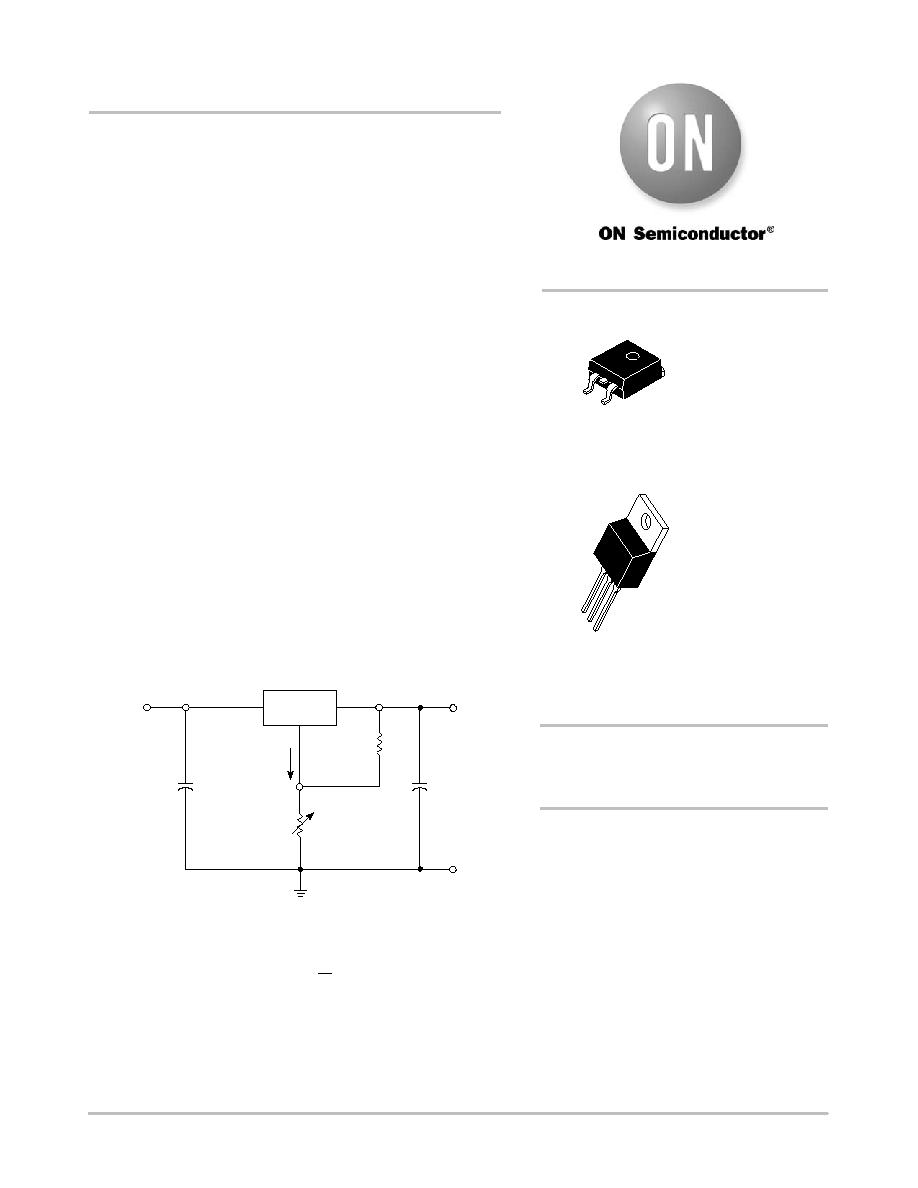
Figure 1. Standard Application
*
* C
in
is required if regulator is located an appreciable distance from power supply filter.
** C
O
is not needed for stability, however, it does improve transient response.
Since I
Adj
is controlled to less than 100
mA, the error associated with this term is
negligible in most applications.
Vout + 1.25 V 1 )
R
2
R
1
) I
Adj
R
2
LM317
V
in
V
out
R
1
240
R
2
Adjust
I
Adj
C
in
*
0.1
mF
+ C
O
**
1.0
mF
TO-220
T SUFFIX
CASE 221A
Pin 1. Adjust
2. V
out
3. V
in
D
2
PAK-3
D2T SUFFIX
CASE 936
Heatsink surface (shown as terminal 4 in
case outline drawing) is connected to Pin 2.
3
1
2
Heatsink surface connected to Pin 2.
3
1
2
http://onsemi.com
See detailed ordering and shipping information in the package
dimensions section on page 10 of this data sheet.
ORDERING INFORMATION
See general marking information in the device marking
section on page 10 of this data sheet.
DEVICE MARKING INFORMATION
LM317, NCV317
http://onsemi.com
2
MAXIMUM RATINGS
Rating
Symbol
Value
Unit
Input-Output Voltage Differential
V
I
-V
O
40
Vdc
Power Dissipation
Case 221A
T
A
= +25
∞
C
P
D
Internally Limited
W
Thermal Resistance, Junction-to-Ambient
q
JA
65
∞
C/W
Thermal Resistance, Junction-to-Case
q
JC
5.0
∞
C/W
Case 936 (D
2
PAK-3)
T
A
= +25
∞
C
P
D
Internally Limited
W
Thermal Resistance, Junction-to-Ambient
q
JA
70
∞
C/W
Thermal Resistance, Junction-to-Case
q
JC
5.0
∞
C/W
Operating Junction Temperature Range
T
J
-55 to +150
∞
C
Storage Temperature Range
T
stg
-65 to +150
∞
C
Maximum ratings are those values beyond which device damage can occur. Maximum ratings applied to the device are individual stress limit
values (not normal operating conditions) and are not valid simultaneously. If these limits are exceeded, device functional operation is not implied,
damage may occur and reliability may be affected.
ELECTRICAL CHARACTERISTICS
(V
I
-V
O
= 5.0 V; I
O
= 0.5 A for D2T and T packages; T
J
= T
low
to T
high
(Note 1); I
max
and P
max
(Note 2); unless otherwise noted.)
Characteristics
Figure
Symbol
Min
Typ
Max
Unit
Line Regulation (Note 3), T
A
= +25
∞
C, 3.0 V
V
I
-V
O
40 V
1
Reg
line
-
0.01
0.04
%/V
Load Regulation (Note 3), T
A
= +25
∞
C, 10 mA
I
O
I
max
V
O
5.0 V
V
O
5.0 V
2
Reg
load
-
-
5.0
0.1
25
0.5
mV
% V
O
Thermal Regulation, T
A
= +25
∞
C (Note 4), 20 ms Pulse
Reg
therm
-
0.03
0.07
% V
O
/W
Adjustment Pin Current
3
I
Adj
-
50
100
m
A
Adjustment Pin Current Change, 2.5 V
V
I
-V
O
40 V,
10 mA
I
L
I
max
, P
D
P
max
1, 2
D
I
Adj
-
0.2
5.0
m
A
Reference Voltage, 3.0 V
V
I
-V
O
40 V,
10 mA
I
O
I
max
, P
D
P
max
3
V
ref
1.2
1.25
1.3
V
Line Regulation (Note 3), 3.0 V
V
I
-V
O
40 V
1
Reg
line
-
0.02
0.07
% V
Load Regulation (Note 3), 10 mA
I
O
I
max
V
O
5.0 V
V
O
5.0 V
2
Reg
load
-
-
20
0.3
70
1.5
mV
% V
O
Temperature Stability (T
low
T
J
T
high
)
3
T
S
-
0.7
-
% V
O
Minimum Load Current to Maintain Regulation (V
I
-V
O
= 40 V)
3
I
Lmin
-
3.5
10
mA
Maximum Output Current
V
I
-V
O
15 V, P
D
P
max,
T Package
V
I
-V
O
= 40 V, P
D
P
max
, T
A
= +25
∞
C, T Package
3
I
max
1.5
0.15
2.2
0.4
-
-
A
RMS Noise, % of V
O
, T
A
= +25
∞
C, 10 Hz
f
10 kHz
N
-
0.003
-
% V
O
Ripple Rejection, V
O
= 10 V, f = 120 Hz (Note 5)
Without C
Adj
C
Adj
= 10
m
F
4
RR
-
66
65
80
-
-
dB
Long-Term Stability, T
J
= T
high
(Note 6), T
A
= +25
∞
C for
Endpoint Measurements
3
S
-
0.3
1.0
%/1.0 k
Hrs.
Thermal Resistance Junction-to-Case, T Package
R
q
JC
-
5.0
-
∞
C/W
1. T
low
to T
high
= 0
∞
to +125
∞
C, for LM317T, D2T. T
low
to T
high
= - 40
∞
to +125
∞
C, for LM317BT, BD2T, T
low
to T
high
= - 55
∞
to +150
∞
C, for
NCV317BT, BD2T.
2. I
max
= 1.5 A, P
max
= 20 W
3. Load and line regulation are specified at constant junction temperature. Changes in V
O
due to heating effects must be taken into account
separately. Pulse testing with low duty cycle is used.
4. Power dissipation within an IC voltage regulator produces a temperature gradient on the die, affecting individual IC components on the die.
These effects can be minimized by proper integrated circuit design and layout techniques. Thermal Regulation is the effect of these
temperature gradients on the output voltage and is expressed in percentage of output change per watt of power change in a specified time.
5. C
Adj
, when used, is connected between the adjustment pin and ground.
6. Since Long-Term Stability cannot be measured on each device before shipment, this specification is an engineering estimate of average
stability from lot to lot.
LM317, NCV317
http://onsemi.com
3
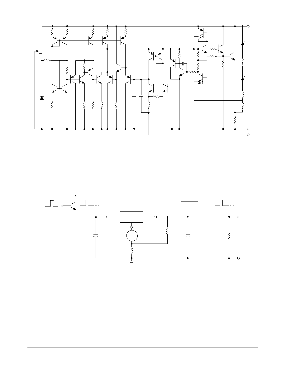
Figure 2. Representative Schematic Diagram
This device contains 29 active transistors.
310
310
230
120
5.6 k
V
in
170
6.3 V
160
12 k
5.0 pF
6.8 k
13 k
6.3 V
105
4.0
0.1
V
out
Adjust
12.5 k
2.4 k
30pF
6.3 V
125 k
135
190
12.4 k
3.6 k 5.8 k 110
5.1 k
6.7 k
510
200
30pF
Figure 3. Line Regulation and
D
I
Adj
/Line Test Circuit
* Pulse testing required.
*
1% Duty Cycle
*
is suggested.
*
V
CC
V
IH
V
IL
V
in
V
out
R
L
+
1.0
mF
C
O
240
1%
R
1
Adjust
R
2
1%
C
in
0.1
mF
I
Adj
LM317
Line Regulation (% V)
+
|V
OH
≠V
OL
|
|V
OL
|
x 100
V
OH
V
OL
LM317, NCV317
http://onsemi.com
4
Figure 4. Load Regulation and
D
I
Adj
/Load Test Circuit
Figure 5. Standard Test Circuit
Figure 6. Ripple Rejection Test Circuit
V
O
LM317
V
O
(min Load)
- V
O
(max Load)
* Pulse testing required.
*
1% Duty Cycle is suggested.
Load Regulation (mV) = V
O
(min Load) - V
O
(max Load)
Load Regulation (% V
O
) =
x 100
V
O
(min Load)
V
O
(max Load)
C
in
0.1
mF
Adjust
R
2
1%
C
O
1.0
mF
+
*
R
L
(max Load)
R
L
(min Load)
V
out
R
1
240
1%
V
I
V
in
I
Adj
I
L
* Pulse testing required.
*
1% Duty Cycle is suggested.
V
in
V
out
Adjust
R
1
240
1%
+
1.0
mF
C
O
R
L
C
in
R
2
1%
To Calculate R
2
: V
out
= I
SET
R
2
+ 1.250 V
To Calculate R
2
:
Assume I
SET
= 5.25 mA
I
L
I
Adj
I
SET
V
ref
V
O
V
I
0.1
mF
V
in
V
out
V
out
= 10 V
R
L
C
in
0.1
mF
Adjust
R
1
240
1%
D
1
*
1N4002
C
O
+
1.0
mF
24 V
14 V
R
2
1.65 k
1%
C
Adj
10
mF
+
* D
1
Discharges C
Adj
if output is shorted to Ground.
f = 120 Hz
LM317
LM317
V
O
(min Load)
LM317, NCV317
http://onsemi.com
5
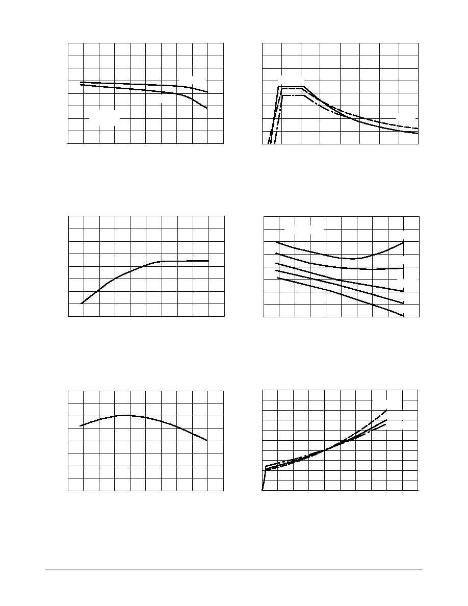
Figure 7. Load Regulation
Figure 8. Current Limit
Figure 9. Adjustment Pin Current
Figure 10. Dropout Voltage
Figure 11. Temperature Stability
Figure 12. Minimum Operating Current
V
out
,
OUTPUT
VOL
T
AGE CHANGE (%)
V
in
= 15 V
V
out
= 10 V
I out
, OUTPUT
CURRENT
(A)
,
ADJUSTMENT
PIN
CURRENT
(
A)
Adj
I
, INPUT-OUTPUT
VOL
T
AGE
in
out
V-
V
ref
V
,
REFERENCE VOL
T
AGE
(V)
I B
, QUIESCENT
CURRENT
(mA)
DIFFERENTIAL
(Vdc)
0.4
0.2
0
-0.2
-0.4
-0.6
-0.8
-1.0
4.0
3.0
2.0
1.0
0
70
65
60
55
50
45
40
35
3.0
2.5
2.0
1.5
1.0
1.26
1.25
1.24
1.23
1.22
5.0
4.5
4.0
3.5
3.0
2.5
2.0
1.5
1.0
0.5
0
-50
-25
0
25
50
75
100
125
150
T
J
, JUNCTION TEMPERATURE (
∞C)
0
10
20
30
40
V
in
-V
out
, INPUT-OUTPUT VOLTAGE DIFFERENTIAL (Vdc)
-50
-25
0
25
50
75
100
125
150
T
J
, JUNCTION TEMPERATURE (
∞C)
-50
-25
0
25
50
75
100
125
150
T
J
, JUNCTION TEMPERATURE (
∞C)
-50
-25
0
25
50
75
100
125
150
T
J
, JUNCTION TEMPERATURE (
∞C)
0
10
20
30
40
V
in
-V
out
, INPUT-OUTPUT VOLTAGE DIFFERENTIAL (Vdc)
1.0 A
+150
∞C
I
L
= 0.5 A
I
L
= 1.5 A
-55
∞C
150
∞C
T
J
= 25
∞C
DV
out
= 100 mV
I
L
= 1.5 A
500 mA
200 mA
20 mA
+25
∞C
T
J
= -55
∞C