
©
Semiconductor Components Industries, LLC, 2003
August, 2003 - Rev. 1
1
Publication Order Number:
NCV4279B/D
NCV4279B
5.0 V Micropower 150 mA
LDO Linear Regulator with
DELAY, Adjustable RESET,
and Monitor FLAG
The NCV4279B is a 5.0 V precision micropower voltage regulator.
The output current capability is 150 mA.
The output voltage is accurate within
±
2.0% with a maximum
dropout voltage of 0.6 V at 150 mA. Low quiescent current is a feature
drawing only 90
mA with a 100 mA load. This part is ideal for any and
all battery operated microprocessor equipment.
Microprocessor control logic includes an active RESET (with
DELAY), and a FLAG monitor which can be used to provide an early
warning signal to the microprocessor of a potential impending RESET
signal. The use of the FLAG monitor allows the microprocessor to
finish any signal processing before the RESET shuts the
microprocessor down.
The active RESET circuit operates correctly at an output voltage as
low as 1.0 V. The RESET function is activated during the power up
sequence or during normal operation if the output voltage drops
outside the regulation limits.
The reset threshold voltage can be decreased by the connection of
external resistor divider to R
ADJ
lead.
The regulator is protected against reverse battery, short circuit, and
thermal overload conditions. The device can withstand load dump
transients making it suitable for use in automotive environments. The
device has also been optimized for EMC conditions.
Features
∑
5.0 V
±
2.0% Output
∑
Low 90
mA Quiescent Current
∑
Active RESET
∑
Adjustable Reset
∑
150 mA Output Current Capability
∑
Fault Protection
-
+60 V Peak Transient Voltage
-
-15 V Reverse Voltage
-
Short Circuit
-
Thermal Overload
∑
Early Warning through FLAG/MON Leads
∑
Internally Fused Leads in SO-14 and SO-20L Packages
∑
NCV Prefix for Automotive and Other Applications Requiring Site
and Control Changes
http://onsemi.com
SO-20L
DW SUFFIX
CASE 751D
1
20
SO-14
D SUFFIX
CASE 751A
1
14
PIN CONNECTIONS
FLAG
RESET
V
OUT
NC
GND
GND
GND
GND
1
14
GND
GND
V
IN
DELAY
MON
R
ADJ
MARKING DIAGRAMS
1
NCV4279B
AWLYWW
14
A
= Assembly Location
WL, L
= Wafer Lot
YY, Y
= Year
WW, W = Work Week
1
NCV4279B
AWLYYWW
20
1
20
NC
NC
GND
GND
GND
GND
GND
GND
GND
GND
NC
NC
V
IN
DELAY
MON
R
ADJ
V
OUT
NC
FLAG
RESET
SO-20L
SO-14
SO-8
D SUFFIX
CASE 751
1
8
1
4279B
ALYW
8
GND
DELAY
1
8
RESET
R
ADJ
FLAG
MON
V
OUT
V
IN
SO-8
ORDERING INFORMATION
See detailed ordering and shipping information in the package
dimensions section on page 10 of this data sheet.

NCV4279B
http://onsemi.com
2
V
OUT
GND
V
IN
R
ADJ
NCV4279B
10
µ
F
10 k
R
RST
RESET
10
µ
F
Microprocessor
Delay
C
DELAY
V
BAT
V
DD
FLAG
Figure 1. Application Diagram
MON
R
FLG
10 k
I/O
I/O
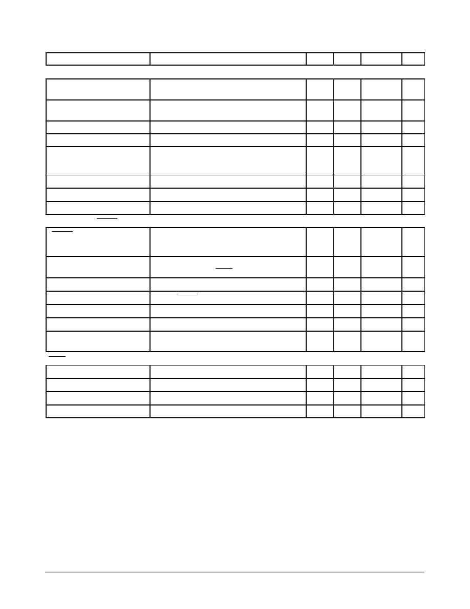
MAXIMUM RATINGS*
{
Rating
Value
Unit
V
IN
(DC)
-15 to 45
V
Peak Transient Voltage (46 V Load Dump @ V
IN
= 14 V)
60
V
Operating Voltage
45
V
V
OUT
(DC)
16
V
Voltage Range (RESET, FLAG)
-0.3 to 10
V
Input Voltage Range (MON)
-0.3 to 10
V
ESD Susceptibility (Human Body Model)
2.0
kV
Junction Temperature, T
J
-40 to +150
∞
C
Storage Temperature, T
S
-55 to 150
∞
C
Package Thermal Resistance, SO-8:
Junction-to-Case, R
JC
Junction-to-Ambient, R
JA
45
165
∞
C/W
Package Thermal Resistance, SO-14 (Fused) Minimum Pad Data:
Junction-to-Case, R
JC
Junction-to-Ambient, R
JA
Junction-to-Pin, R
JP
(Note 3)
15
110
33
∞
C/W
Package Thermal Resistance, SO-20L (Fused) Minimum Pad Data:
Junction-to-Case, R
JC
Junction-to-Ambient, R
JA
Junction-to-Pin, R
JP
(Note 4)
12
82
26
∞
C/W
Lead Temperature Soldering:
Reflow: (SMD styles only) (Notes 1, 2)
240 peak
∞
C
1. 60 second maximum above 183
∞
C.
2. -5
∞
C/+0
∞
C allowable conditions.
3. Measured to pin 9.
4. Measured to pin 12.
*The maximum package power dissipation must be observed.
During the voltage range which exceeds the maximum tested voltage of V
IN
, operation is assured, but not specified. Wider limits may apply.
Thermal dissipation must be observed closely.
NCV4279B
http://onsemi.com
3
ELECTRICAL CHARACTERISTICS
(I
OUT
= 1.0 mA, -40
∞
C
T
J
125
∞
C; 6.0 V < V
IN
< 26 V; unless otherwise specified.)
Characteristic
Test Conditions
Min
Typ
Max
Unit
Output Stage
Output Voltage
9.0 V < V
IN
< 16 V, 100
m
A
I
OUT
150 mA
6.0 V < V
IN
< 26 V, 100
m
A
I
OUT
150 mA
4.90
4.85
5.0
5.0
5.10
5.15
V
V
Dropout Voltage (V
IN
- V
OUT
)
I
OUT
= 150 mA
I
OUT
= 100
m
A
-
-
400
100
600
150
mV
mV
Load Regulation
V
IN
= 14 V, 5.0 mA
I
OUT
150 mA
-30
5.0
30
mV
Line Regulation
[V
OUT
(typ) + 1.0] < V
IN
< 26 V, I
OUT
= 1.0 mA
-
15
60
mV
Quiescent Current, (I
Q
)
Active Mode
I
OUT
= 100
m
A, V
IN
= 12 V, Delay = 3.0 V, MON = 3.0 V
I
OUT
= 75 mA, V
IN
= 14 V, Delay = 3.0 V, MON = 3.0 V
I
OUT
150 mA, V
IN
= 14 V, Delay = 3.0 V, MON = 3.0 V
-
-
-
90
4.0
12
125
6.0
19
m
A
mA
mA
Current Limit
-
151
300
-
mA
Short Circuit Output Current
V
OUT
= 0 V
40
190
-
mA
Thermal Shutdown
(Guaranteed by Design)
150
180
-
∞
C
Reset Function (RESET)
RESET Threshold
HIGH (V
RH
)
LOW (V
RL
)
V
OUT
Increasing
V
OUT
Decreasing
4.55
4.50
4.70
4.60
0.98
◊
V
OUT
0.97
◊
V
OUT
V
V
Output Voltage
Low (V
RLO
)
1.0 V
V
OUT
V
RL
, R
RESET
= 10 k
-
0.1
0.4
V
Delay Switching Threshold (V
DT
)
-
1.4
1.8
2.2
V
Reset Delay Low Voltage
V
OUT
< RESET Threshold Low(min)
-
-
0.1
V
Delay Charge Current
DELAY = 1.0 V, V
OUT
> V
RH
1.5
2.5
3.5
m
A
Delay Discharge Current
DELAY = 1.0 V, V
OUT
= 1.5 V
5.0
-
-
mA
Reset Adjust Switching Voltage
(V
R(ADJ)
)
-
1.23
1.31
1.39
V
FLAG/Monitor
Monitor Threshold
Increasing and Decreasing
1.10
1.20
1.31
V
Hysteresis
-
20
50
100
mV
Input Current
MON = 2.0 V
-0.5
0.1
0.5
m
A
Output Saturation Voltage
MON = 0 V, I
FLAG
= 1.0 mA
-
0.1
0.4
V

NCV4279B
http://onsemi.com
4
PACKAGE PIN DESCRIPTION
Package Pin Number
SO-8
SO-14
SO-20L
Pin Symbol
Function
3
1
1
R
ADJ
Reset Adjust. If not needed connect to ground.
4
2
2
DELAY
Timing capacitor for RESET function.
5
3-5, 10-12
4-7, 14-17
GND
Ground. All GND leads must be connected to Ground
.
-
6
3, 8, 9, 13, 18
NC
No connection.
6
7
10
RESET
Active reset (accurate to V
OUT
1.0 V)
7
8
11
FLAG
Open collector output from early warning comparator.
8
9
12
V
OUT
±
2.0%, 150 mA output.
1
13
19
V
IN
Input Voltage.
2
14
20
MON
Monitor. Input for early warning comparator. If not needed connect to V
OUT.
TYPICAL PERFORMANCE CHARACTERISTICS
-40
V
OUT
(V)
4.98
Temperature (
∞
C)
4.99
5.00
5.01
-25 -10
125
5
20
35
50
65
80
95
110
V
OUT
= 5.0 V
V
IN
= 14 V
I
OUT
= 5.0 mA
Figure 2. Output Voltage vs. Temperature
Figure 3. Quiescent Current vs. Output Current
Figure 4. Quiescent Current vs. Output Current
+25
∞
C
-40
∞
C
0
I
Q
(mA)
0
I
OUT
(mA)
0.2
0.4
0.6
0.8
1.0
1.2
5
10
15
20
25
+125
∞
C
V
IN
= 12 V
0
I
Q
(mA)
0
I
OUT
(mA)
2
4
6
8
10
12
14
15
30
45
60
140
75
90
105 120 135
+25
∞
C
-40
∞
C
+125
∞
C
V
IN
= 12 V
6
I
Q
(mA)
0
V
IN
(V)
1
2
3
4
5
6
7
8
10
12
14
26
16
18
20
22
24
I
OUT
= 10 mA
I
OUT
= 50 mA
I
OUT
= 100 mA
T = 25
∞
C
Figure 5. Quiescent Current vs. Input Voltage

NCV4279B
http://onsemi.com
5
TYPICAL PERFORMANCE CHARACTERISTICS
Figure 6. Quiescent Current vs. Input Voltage
I
OUT
= 100
m
A
6
I
Q
(
µ
A)
0
V
IN
(V)
20
49
60
80
100
120
8
10
12
14
26
16
18
20
22
24
T = 25
∞
C
+25
∞
C
-40
∞
C
+125
∞
C
0
Dropout V
oltage (mV)
0
I
OUT
(mA)
150
200
250
300
350
400
450
25
50
75
100
150
50
100
125
Figure 7. Dropout Voltage vs. Output Current
1
10
100
1000
0
10 20 30 40 50 60 70 80 90 100110120130140150
Unstable Region
Stable Region
C
Vout
= 10
m
F
Figure 8. Output Capacitor ESR
ESR (
W
)
OUTPUT CURRENT (mA)
Figure 9. Output Stability with Output
Capacitor Change
0.01
0.1
1
10
100
1000
0
10
20
30
50
60
70
80
90
100 110
OUTPUT CURRENT (mA)
ESR (
W
)
C
Vout
= 10
m
F
C
Vout
= 0.1
m
F
Unstable Region
Stable Region
40