©
Semiconductor Components Industries, LLC, 2004
September, 2004 - Rev. 19
1
Publication Order Number:
NCV8501/D
NCV8501 Series
Micropower 150 mA LDO
Linear Regulators
with ENABLE, DELAY,
RESET, and Monitor FLAG
The NCV8501 is a family of precision micropower voltage
regulators. Their output current capability is 150 mA. The family has
output voltage options for adjustable, 2.5 V, 3.3 V, 5.0 V, 8.0 V, and 10 V.
The output voltage is accurate within
±
2.0% with a maximum
dropout voltage of 0.6 V at 150 mA. Low quiescent current is a feature
drawing only 90
mA with a 100 mA load. This part is ideal for any and
all battery operated microprocessor equipment.
Microprocessor control logic includes an active RESET (with
DELAY), and a FLAG monitor which can be used to provide an early
warning signal to the microprocessor of a potential impending RESET
signal. The use of the FLAG monitor allows the microprocessor to
finish any signal processing before the RESET shuts the
microprocessor down.
The active RESET circuit operates correctly at an output voltage as
low as 1.0 V. The RESET function is activated during the power up
sequence or during normal operation if the output voltage drops
outside the regulation limits.
The regulator is protected against reverse battery, short circuit, and
thermal overload conditions. The device can withstand load dump
transients making it suitable for use in automotive environments. The
device has also been optimized for EMC conditions.
Features
∑
Output Voltage Options: Adjustable, 2.5 V, 3.3 V, 5.0 V, 8.0 V, 10 V
∑
±
2.0% Output
∑
Low 90
mA Quiescent Current
∑
Fixed or Adjustable Output Voltage
∑
Active RESET
∑
ENABLE
∑
150 mA Output Current Capability
∑
Fault Protection
+60 V Peak Transient Voltage
-15 V Reverse Voltage
Short Circuit
Thermal Overload
∑
Early Warning through FLAG/MON Leads
∑
NCV Prefix for Automotive and Other Applications Requiring Site
and Change Control
∑
Pb-Free Packages are Available
SO-8
D SUFFIX
CASE 751
1
8
See detailed ordering and shipping information in the package
dimensions section on page 13 of this data sheet.
ORDERING INFORMATION
SOIC 16 LEAD
WIDE BODY
EXPOSED PAD
PDW SUFFIX
CASE 751R
1
16
http://onsemi.com
1
8501x
ALYW
8
SO-8
SOW-16
E PAD
8501x
AWLYYWW
1
16
x
= Voltage Ratings as Indicated Below:
A = Adjustable
2 = 2.5 V
3 = 3.3 V
5 = 5.0 V
8 = 8.0 V
1 = 10 V
A
= Assembly Location
WL, L
= Wafer Lot
YY, Y
= Year
WW, W = Work Week
MARKING DIAGRAMS
NCV8501 Series
http://onsemi.com
2
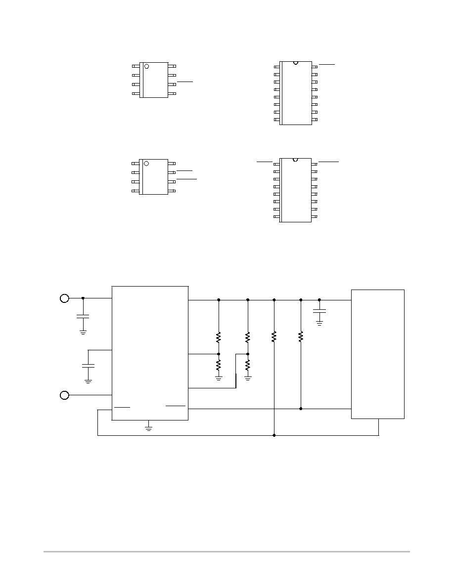
GND
NC
1
8
FLAG
ENABLE
V
ADJ
MON
V
OUT
V
IN
PIN CONNECTIONS, ADJUSTABLE OUTPUT
SO-8
GND
DELAY
1
8
RESET
ENABLE
FLAG
MON
V
OUT
V
IN
PIN CONNECTIONS, FIXED OUTPUT
SO-8
ENABLE
MON
1
16
NC
V
IN
NC
NC
NC
NC
GND
NC
NC
NC
NC
V
OUT
FLAG
V
ADJ
SOW-16 E PAD
ENABLE
MON
1
16
DELAY
V
IN
NC
NC
NC
NC
GND
NC
NC
NC
NC
V
OUT
RESET
FLAG
SOW-16 E PAD
V
OUT
GND
V
IN
NCV8501
10
m
F
10 k
R
RST
RESET
10
m
F
Microprocessor
DELAY
C
DELAY
V
BAT
V
DD
FLAG
Figure 1. Application Diagram
MON
R
FLG
10 k
V
ADJ
(Adjustable
Output Only)
I/O
I/O
ENABLE
NCV8501 Series
http://onsemi.com
3
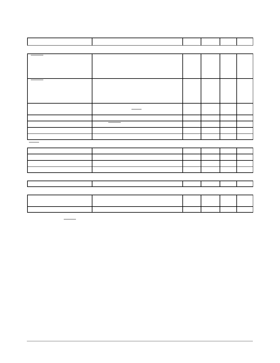
MAXIMUM RATINGS*
Rating
Value
Unit
V
IN
(dc)
-15 to 45
V
Peak Transient Voltage (46 V Load Dump @ V
IN
= 14 V)
60
V
Operating Voltage
45
V
V
OUT
(dc)
16
V
Voltage Range (RESET, FLAG)
-0.3 to 10
V
Input Voltage Range (MON)
-0.3 to 10
V
Input Voltage Range (ENABLE)
-0.3 to 10**
V
ESD Susceptibility (Human Body Model)
2.0
kV
Junction Temperature, T
J
-40 to +150
∞
C
Storage Temperature, T
S
-55 to 150
∞
C
Package Thermal Resistance, SO-8:
Junction-to-Case, R
q
JC
Junction-to-Ambient, R
q
JA
45
165
∞
C/W
∞
C/W
Package Thermal Resistance, SOW-16 E PAD:
Junction-to-Case, R
q
JC
Junction-to-Ambient, R
q
JA
Junction-to-Pin, R
q
JP
(Note 1)
15
56
35
∞
C/W
∞
C/W
∞
C/W
Lead Temperature Soldering:
Reflow: (SMD styles only) (Note 2)
240 peak
260 Peak (Pb-Free)
(Note 3)
∞
C
Maximum ratings are those values beyond which device damage can occur. Maximum ratings applied to the device are individual stress limit
values (not normal operating conditions) and are not valid simultaneously. If these limits are exceeded, device functional operation is not implied,
damage may occur and reliability may be affected.
*During the voltage range which exceeds the maximum tested voltage of V
IN
, operation is assured, but not specified. Wider limits may apply.
Thermal dissipation must be observed closely.
**Reference Figure 14 for switched-battery ENABLE application.
1. Measured to pin 16.
2. 150 second maximum above 183
∞
C, Pb-Free - 150 second maximum above 217
∞
C.
3. -5
∞
C / +0
∞
C allowable conditions, applies to both Pb and Pb-Free devices.
NCV8501 Series
http://onsemi.com
4
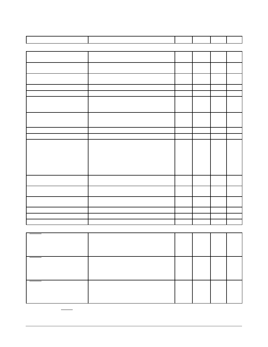
ELECTRICAL CHARACTERISTICS
(I
OUT
= 1.0 mA, ENABLE = 5.0 V, -40
∞
C
T
J
125
∞
C; V
IN
dependent on voltage option
(Note 4); unless otherwise specified.)
Characteristic
Test Conditions
Min
Typ
Max
Unit
Output Stage
Output Voltage for 2.5 V Option
6.5 V < V
IN
< 16 V, 100
m
A
I
OUT
150 mA
5.5 V < V
IN
< 26 V, 100
m
A
I
OUT
150 mA
2.450
2.425
2.5
2.5
2.550
2.575
V
V
Output Voltage for 3.3 V Option
7.3 V < V
IN
< 16 V, 100
m
A
I
OUT
150 mA
5.5 V < V
IN
< 26 V, 100
m
A
I
OUT
150 mA
3.234
3.201
3.3
3.3
3.366
3.399
V
V
Output Voltage for 5.0 V Option
9.0 V < V
IN
< 16 V, 100
m
A
I
OUT
150 mA
6.0 V < V
IN
< 26 V, 100
m
A
I
OUT
150 mA
4.90
4.85
5.0
5.0
5.10
5.15
V
V
Output Voltage for 8.0 V Option
9.0 V < V
IN
< 26 V, 100
m
A
I
OUT
150 mA
7.76
8.0
8.24
V
Output Voltage for 10 V Option
11 V < V
IN
< 26 V, 100
m
A
I
OUT
150 mA
9.7
10
10.3
V
Output Voltage for Adjustable Option
V
OUT
= V
ADJ
(Unity Gain)
6.5 V < V
IN
< 16 V, 100
m
A < I
OUT
< 150 mA
5.5 V < V
IN
< 26 V, 100
m
A < I
OUT
< 150 mA
1.254
1.242
1.280
1.280
1.306
1.318
V
V
Dropout Voltage (V
IN
- V
OUT
)
(5.0 V, 8.0 V, 10 V, and
Adj. > 5.0 V Options Only)
I
OUT
= 150 mA
I
OUT
= 1.0 mA
-
-
400
100
600
150
mV
mV
Load Regulation
V
IN
= 14 V, 5.0 mA
I
OUT
150 mA
-30
5.0
30
mV
Line Regulation
[V
OUT
(Typ) + 1.0] < V
IN
< 26 V, I
OUT
= 1.0 mA
-
15
60
mV
Quiescent Current, Low Load
2.5 V Option
3.3 V Option
5.0 V Option
8.0 V Option
10 V Option
Adjustable Option
I
OUT
= 100
m
A, V
IN
= 12 V, MON = V
OUT
-
-
-
-
-
-
90
90
90
100
100
50
125
125
125
150
150
75
m
A
m
A
m
A
m
A
m
A
m
A
Quiescent Current, Medium Load
All Options
I
OUT
= 75 mA, V
IN
= 14 V, MON = V
OUT
-
4.0
6.0
mA
Quiescent Current, High Load
All Options
I
OUT
= 150 mA, V
IN
= 14 V, MON = V
OUT
-
12
19
mA
Quiescent Current, (I
Q
)
Sleep Mode
ENABLE = 0 V, V
IN
= 12 V
-
12
30
m
A
Current Limit
-
151
300
-
mA
Short Circuit Output Current
V
OUT
= 0 V
40
190
-
mA
Thermal Shutdown
(Guaranteed by Design)
150
180
-
∞
C
Reset Function (RESET)
RESET Threshold for 2.5 V Option
HIGH (V
RH
)
LOW (V
RL
)
5.5 V
V
IN
26 V (Note 5)
V
OUT
Increasing
V
OUT
Decreasing
2.28
2.25
2.350
2.300
0.98
◊
V
OUT
0.97
◊
V
OUT
V
V
RESET Threshold for 3.3 V Option
HIGH (V
RH
)
LOW (V
RL
)
5.5 V
V
IN
26 V (Note 5)
V
OUT
Increasing
V
OUT
Decreasing
3.00
2.97
3.102
3.036
0.98
◊
V
OUT
0.97
◊
V
OUT
V
V
RESET Threshold for 5.0 V Option
HIGH (V
RH
)
LOW (V
RL
)
V
OUT
Increasing
V
OUT
Decreasing
4.55
4.50
4.70
4.60
0.98
◊
V
OUT
0.97
◊
V
OUT
V
V
4. Voltage range specified in the Output Stage of the Electrical Characteristics in boldface type.
5. For V
IN
5.5 V, a RESET = Low may occur with the output in regulation.
NCV8501 Series
http://onsemi.com
5
ELECTRICAL CHARACTERISTICS
(I
OUT
= 1.0 mA, ENABLE = 5.0 V, -40
∞
C
T
J
125
∞
C; V
IN
dependent on voltage option
(Note 4); unless otherwise specified.)
Characteristic
Unit
Max
Typ
Min
Test Conditions
Reset Function (RESET)
RESET Threshold for 8.0 V Option
HIGH (V
RH
)
LOW (V
RL
)
V
OUT
Increasing
V
OUT
Decreasing
6.86
6.80
7.52
7.36
0.98
◊
V
OUT
0.97
◊
V
OUT
V
V
RESET Threshold for 10 V Option
HIGH (V
RH
)
LOW (V
RL
)
V
OUT
Increasing
V
OUT
Decreasing
8.60
8.50
9.40
9.20
0.98
◊
V
OUT
0.97
◊
V
OUT
V
V
Output Voltage
Low (V
RLO
)
1.0 V
V
OUT
V
RL
, R
RESET
= 10 k
-
0.1
0.4
V
DELAY Switching Threshold (V
DT
)
-
1.4
1.8
2.2
V
DELAY Low Voltage
V
OUT
< RESET Threshold Low(min)
-
-
0.1
V
DELAY Charge Current
DELAY = 1.0 V, V
OUT
> V
RH
1.5
2.5
3.5
m
A
DELAY Discharge Current
DELAY = 1.0 V, V
OUT
= 1.5 V
5.0
-
-
mA
FLAG/Monitor
Monitor Threshold
Increasing and Decreasing
1.10
1.20
1.31
V
Hysteresis
-
20
50
100
mV
Input Current
MON = 2.0 V
-0.5
0.1
0.5
m
A
Output Saturation Voltage
MON = 0 V, I
FLAG
= 1.0 mA
-
0.1
0.4
V
Voltage Adjust (Adjustable Output only)
Input Current
V
ADJ
= 1.28 V
-0.5
-
0.5
m
A
ENABLE
Input Threshold
Low
High
-
3.0
-
-
0.5
-
V
V
Input Current
ENABLE = 5.0 V
-
1.0
5.0
m
A
4. Voltage range specified in the Output Stage of the Electrical Characteristics in boldface type.
5. For V
IN
5.5 V, a RESET = Low may occur with the output in regulation.

NCV8501 Series
http://onsemi.com
6
PACKAGE PIN DESCRIPTION, ADJUSTABLE OUTPUT
Package Pin Number
SO-8
SOW-16
E PAD
Pin Symbol
Function
1
7
V
IN
Input Voltage.
2
8
MON
Monitor. Input for early warning comparator. If not needed connect to V
OUT.
3
9
ENABLE
ENABLE control for the IC. A high powers the device up.
4
3-6, 10-12,
14, 15
NC
No connection.
5
13
GND
Ground. All GND leads must be connected to Ground
.
6
16
FLAG
Open collector output from early warning comparator.
7
1
V
ADJ
Voltage Adjust. A resistor divider from V
OUT
to this lead sets the output voltage.
8
2
V
OUT
±
2.0%, 150 mA output.
PACKAGE PIN DESCRIPTION, FIXED OUTPUT
Package Pin Number
SO-8
SOW-16
E PAD
Pin Symbol
Function
1
7
V
IN
Input Voltage.
2
8
MON
Monitor. Input for early warning comparator. If not needed connect to V
OUT.
3
9
ENABLE
ENABLE control for the IC. A high powers the device up.
4
10
DELAY
Timing capacitor for RESET function.
5
13
GND
Ground. All GND leads must be connected to Ground
.
6
16
RESET
Active reset (accurate to V
OUT
1.0 V)
7
1
FLAG
Open collector output from early warning comparator.
8
2
V
OUT
±
2.0%, 150 mA output.
-
3-6, 11, 12,
14, 15
NC
No connection.
NCV8501 Series
http://onsemi.com
7
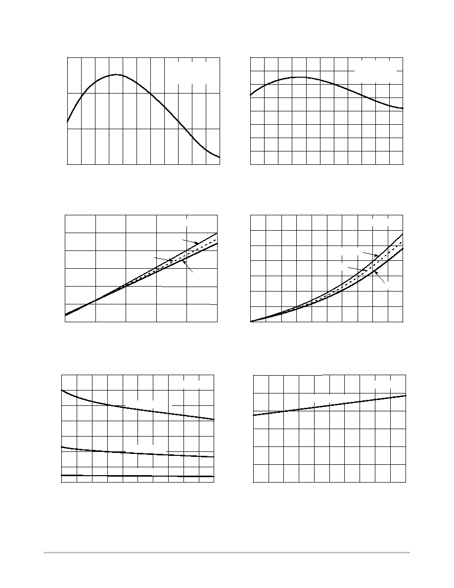
TYPICAL PERFORMANCE CHARACTERISTICS
-40
V
OUT
(V)
4.98
Temperature (
∞
C)
4.99
5.00
5.01
-25 -10
125
5
20
35
50
65
80
95
110
V
OUT
= 5.0 V
V
IN
= 14 V
I
OUT
= 5.0 mA
Figure 2. Output Voltage vs. Temperature
-40
V
OUT
(V)
3.27
Temperature (
∞
C)
3.32
3.33
3.35
-25 -10
125
5
20
35
50
65
80
95
110
3.34
3.29
3.30
3.31
3.28
V
OUT
= 3.3 V
V
IN
= 14 V
I
OUT
= 5.0 mA
Figure 3. Output Voltage vs. Temperature
Figure 4. Quiescent Current vs. Output Current
Figure 5. Quiescent Current vs. Output Current
+25
∞
C
-40
∞
C
0
I
Q
(mA)
0
I
OUT
(mA)
0.2
0.4
0.6
0.8
1.0
1.2
5
10
15
20
25
+125
∞
C
V
IN
= 12 V
0
I
Q
(mA)
0
I
OUT
(mA)
2
4
6
8
10
12
14
15
30
45
60
140
75
90
105 120 135
+25
∞
C
-40
∞
C
+125
∞
C
V
IN
= 12 V
6
I
Q
(mA)
0
V
IN
(V)
1
2
3
4
5
6
7
8
10
12
14
26
16
18
20
22
24
I
OUT
= 10 mA
I
OUT
= 50 mA
I
OUT
= 100 mA
T = 25
∞
C
Figure 6. Quiescent Current vs. Input Voltage
Figure 7. Quiescent Current vs. Input Voltage
I
OUT
= 100
m
A
6
I
Q
(
m
A)
0
V
IN
(V)
20
49
60
80
100
120
8
10
12
14
26
16
18
20
22
24
T = 25
∞
C
NCV8501 Series
http://onsemi.com
8
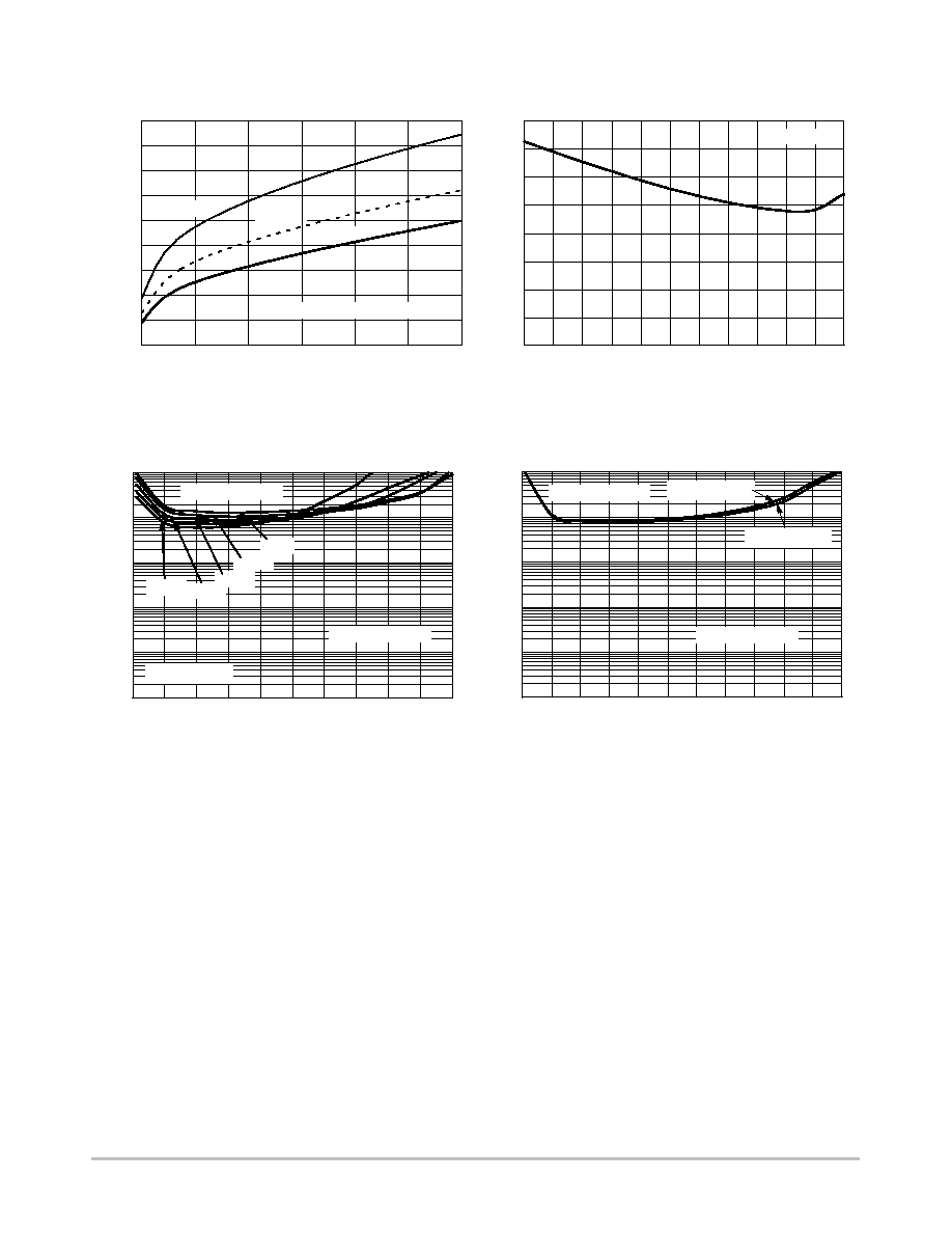
TYPICAL PERFORMANCE CHARACTERISTICS
+25
∞
C
-40
∞
C
+125
∞
C
0
Dropout
V
oltage (mV)
0
I
OUT
(mA)
150
200
250
300
350
400
450
25
50
75
100
150
50
100
125
Figure 8. Dropout Voltage vs. Output Current
V
OUT
= 5.0 V, 8.0 V, or 10 V
Quiescent Current (
m
A)
0
2
4
6
8
10
12
16
14
-40
Temperature (
∞
C)
-25 -10
125
5
20
35
50
65
80
95
110
Figure 9. Sleep Mode I
Q
vs. Temperature
V
IN
= 12 V
0.01
0.1
1.0
10
100
1000
0
10
20
30
50
60
70
80
90
100 110
OUTPUT CURRENT (mA)
ESR (
W
)
C
Vout
= 10
m
F
C
Vout
= 0.1
m
F
Unstable Region
Stable Region
40
0.01
0.1
1.0
10
100
1000
0
10
20
30
40
50
60
70
80
90
100
OUTPUT CURRENT (mA)
ESR (
W
)
C
VOUT
= 10
m
F
10 V
8 V
5 V
3.3 V
2.5 V
Unstable Region
Stable Region
Figure 10. Output Stability with Output
Voltage Change
Figure 11. Output Stability with Output
Capacitor Change
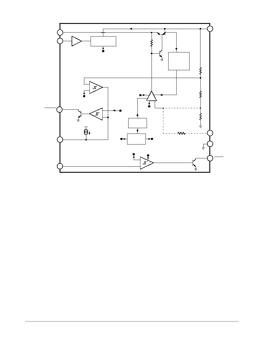
NCV8501 Series
http://onsemi.com
9
V
IN
RESET
V
OUT
FLAG
Delay
Figure 12. Block Diagram
GND
MON
Current Source
(Circuit Bias)
Current Limit
Sense
Error Amplifier
V
BG
I
BIAS
V
BG
V
BG
I
BIAS
I
BIAS
V
BG
I
BIAS
+ -
+
-
+
-
+
-
+
Bandgap
Reference
Thermal
Protection
1.8 V
3.0
m
A
20 k
Adjustable
Version only
V
ADJ
ENABLE
Fixed Voltage only
NCV8501 Series
http://onsemi.com
10
CIRCUIT DESCRIPTION
REGULATOR CONTROL FUNCTIONS
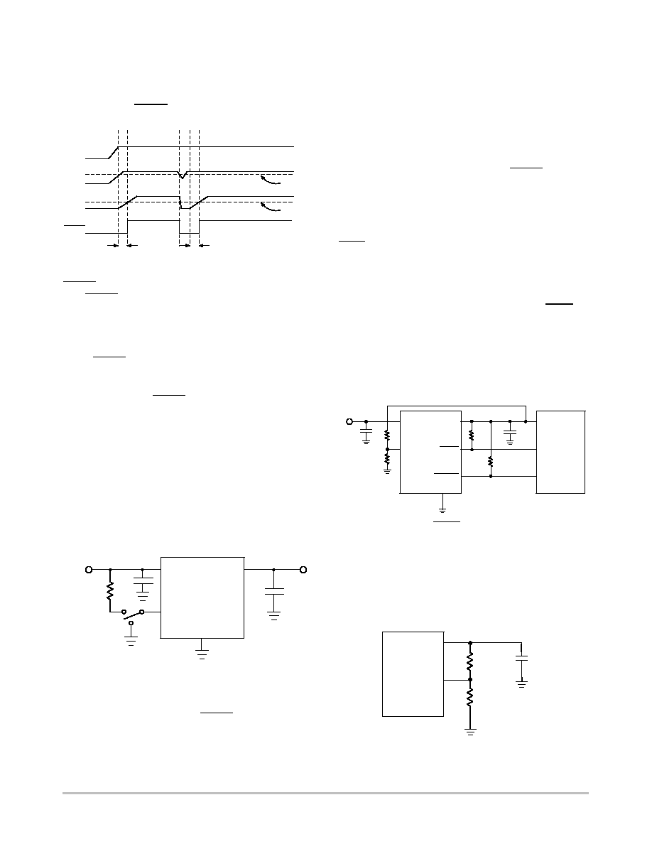
The NCV8501 contains the microprocessor compatible
control function RESET (Figure 13).
Figure 13. Reset and Delay Circuit Wave Forms
V
IN
V
OUT
RESET
DELAY
(V
DT
)
Threshold
DELAY
Threshold
RESET
T
d
T
d
RESET Function
A RESET signal (low voltage) is generated as the IC
powers up until V
OUT
is within 6.0% of the regulated output
voltage, or when V
OUT
drops out of regulation,and is lower
than 8.0% below the regulated output voltage. Hysteresis is
included in the function to minimize oscillations.
The RESET output is an open collector NPN transistor,
controlled by a low voltage detection circuit. The circuit is
functionally independent of the rest of the IC thereby
guaranteeing that the RESET signal is valid for V
OUT
as low
as 1.0 V.
ENABLE Function
The part stays in a low I
Q
sleep mode when the ENABLE
pin is held low. The part has an internal pull down if the pin
is left floating. This is intended for failure modes only. An
external connection (active pulldown, resistor, or switch) for
normal operation is recommended.
The integrity of the ENABLE pin allows it to be tied
directly to the battery line through an external resistor. It will
withstand load dump potentials in this configuration.
Figure 14. ENABLE Function
V
IN
V
OUT
GND
NCV8501
ENABLE
V
BAT
10 k
DELAY Function
The reset delay circuit provides a programmable (by
external capacitor) delay on the RESET output lead.
The DELAY lead provides source current (typically 2.5
mA)
to the external DELAY capacitor during the following
proceedings:
1. During Power Up (once the regulation threshold
has been verified).
2. After a reset event has occurred and the device is
back in regulation. The DELAY capacitor is
discharged when the regulation (RESET threshold)
has been violated. This is a latched incident. The
capacitor will fully discharge and wait for the
device to regulate before going through the delay
time event again.
FLAG/Monitor Function
An on-chip comparator is provided to perform an early
warning to the microprocessor of a possible reset signal. The
reset signal typically turns the microprocessor off
instantaneously. This can cause unpredictable results with
the microprocessor. The signal received from the FLAG pin
will allow the microprocessor time to complete its present
task before shutting down. This function is performed by a
comparator referenced to the bandgap reference. The actual
trip point can be programmed externally using a resistor
divider to the input monitor (MON) (Figure 15). The typical
threshold is 1.20 V on the MON pin.
Figure 15. FLAG/Monitor Function
V
BAT
V
IN
MON
V
OUT
C
OUT
V
CC
I/O
RESET
m
P
FLAG
RESET
GND
DELAY
NCV8501
R
ADJ
Voltage Adjust
Figure 16 shows the device setup for a user configurable
output voltage. The feedback to the V
ADJ
pin is taken from
a voltage divider referenced to the output voltage. The loop
is balanced around the Unity Gain threshold (1.28 V
typical).
Figure 16. Adjustable Output Voltage
V
OUT
V
ADJ
NCV8501
15 k
5.1 k
C
OUT
5.0 V
1.28 V

NCV8501 Series
http://onsemi.com
11
APPLICATION NOTES
Figure 17. Additional Output Current
NCV8501
V
IN
V
OUT
V
ADJ
C2
0.1
m
F
V
BAT
5.0 V
MJD31C
R1
294 k
R2
100 k
C1
47
m
F
>1 Amp
Adding Capability
Figure 17 shows how the adjustable version of parts can
be used with an external pass transistor for additional current
capability. The setup as shown will provide greater than 1
Amp of output current.
FLAG MONITOR
Figure 18 shows the FLAG Monitor waveforms as a result
of the circuit depicted in Figure 15. As the output voltage
falls (V
OUT
), the Monitor threshold is crossed. This causes
the voltage on the FLAG output to go low sending a warning
signal to the microprocessor that a RESET signal may occur
in a short period of time. T
WARNING
is the time the
microprocessor has to complete the function it is currently
working on and get ready for the RESET shutdown signal.
Figure 18. FLAG Monitor Circuit Waveform
V
OUT
MON
RESET
FLAG Monitor
Ref. Voltage
T
WARNING
FLAG
Figure 19. Test and Application Circuit Showing
Output Compensation
V
IN
V
OUT
C
OUT
**
10
m
F
R
RST
RESET
C
IN
*
0.1
m
F
NCV8501
*C
IN
required if regulator is located far from the power supply filter
**C
OUT
required for stability. Capacitor must operate at minimum
temperature expected
SETTING THE DELAY TIME
The delay time is controlled by the Reset Delay Low
Voltage, Delay Switching Threshold, and the Delay Charge
Current. The delay follows the equation:
tDELAY
+
[CDELAY(Vdt
*
Reset Delay Low Voltage)]
Delay Charge Current
Example:
Using C
DELAY
= 33 nF.
Assume reset Delay Low Voltage = 0.
Use the typical value for V
dt
= 1.8 V.
Use the typical value for Delay Charge Current = 2.5
mA.
tDELAY
+
[33 nF(1.8
*
0)]
2.5
m
A
+
23.8 ms
STABILITY CONSIDERATIONS
The output or compensation capacitor helps determine
three main characteristics of a linear regulator: start-up
delay, load transient response and loop stability.
The capacitor value and type should be based on cost,
availability, size and temperature constraints. A tantalum or
aluminum electrolytic capacitor is best, since a film or
ceramic capacitor with almost zero ESR can cause
instability. The aluminum electrolytic capacitor is the least
expensive solution, but, if the circuit operates at low
temperatures (-25
∞
C to -40
∞
C), both the value and ESR of
the capacitor will vary considerably. The capacitor
manufacturers data sheet usually provides this information.
The value for the output capacitor C
OUT
shown in Figure 19
should work for most applications, however it is not
necessarily the optimized solution.
NCV8501 Series
http://onsemi.com
12
CALCULATING POWER DISSIPATION IN A
SINGLE OUTPUT LINEAR REGULATOR
The maximum power dissipation for a single output
regulator (Figure 20) is:
PD(max)
+
[VIN(max)
*
VOUT(min)]IOUT(max)
)
VIN(max)IQ
(eq. 1)
where:
V
IN(max)
is the maximum input voltage,
V
OUT(min)
is the minimum output voltage,
I
OUT(max)
is the maximum output current for the
application, and
I
Q
is the quiescent current the regulator consumes at
I
OUT(max)
.
Once the value of P
D(max)
is known, the maximum
permissible value of R
qJA
can be calculated:
R
Q
JA
+
150
∞
C
*
TA
PD
(eq. 2)
The value of R
qJA
can then be compared with those in the
package section of the data sheet. Those packages with
R
qJA
's less than the calculated value in Equation 2 will keep
the die temperature below 150
∞
C.
In some cases, none of the packages will be sufficient to
dissipate the heat generated by the IC, and an external
heatsink will be required.
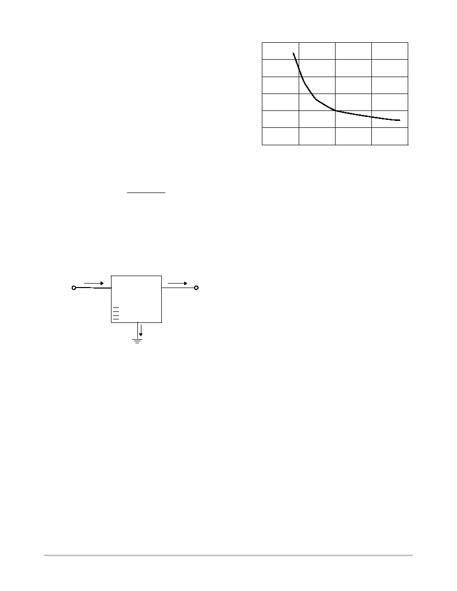
SMART
REGULATOR
Æ
I
Q
Control
Features
I
OUT
I
IN
Figure 20. Single Output Regulator with Key
Performance Parameters Labeled
V
IN
V
OUT
}
Figure 21. 16 Lead SOW (Exposed Pad),
q
JA as a
Function of the Pad Copper Area (2 oz. Cu
Thickness), Board Material = 0.0625
,
G-10/R-4
40
70
90
100
Thermal
Resistance,
Junction to Ambient, R
q
JA
, (
∞
C/W)
0
Copper Area (mm
2
)
200
400
800
80
60
50
600
HEATSINKS
A heatsink effectively increases the surface area of the
package to improve the flow of heat away from the IC and
into the surrounding air.
Each material in the heat flow path between the IC and the
outside environment will have a thermal resistance. Like
series electrical resistances, these resistances are summed to
determine the value of R
qJA
:
R
q
JA
+
R
q
JC
)
R
q
CS
)
R
q
SA
(eq. 3)
where:
R
qJC
= the junction-to-case thermal resistance,
R
qCS
= the case-to-heatsink thermal resistance, and
R
qSA
= the heatsink-to-ambient thermal resistance.
R
qJC
appears in the package section of the data sheet. Like
R
qJA
, it too is a function of package type. R
qCS
and R
qSA
are
functions of the package type, heatsink and the interface
between them. These values appear in heatsink data sheets
of heatsink manufacturers.
NCV8501 Series
http://onsemi.com
13
ORDERING INFORMATION
Device
Output Voltage
Package
Shipping
NCV8501DADJ
Adjustable
SO-8
98 Units/Rail
NCV8501DADJG
Adjustable
SO-8
(Pb-Free)
98 Units/Rail
NCV8501DADJR2
Adjustable
SO-8
2500 Tape & Reel
NCV8501DADJR2G
Adjustable
SO-8
(Pb-Free)
2500 Tape & Reel
NCV8501PDWADJ
Adjustable
SOW-16 Exposed Pad
47 Units/Rail
NCV8501PDWADJR2
Adjustable
SOW-16 Exposed Pad
1000 Tape & Reel
NCV8501D25
2.5 V
SO-8
98 Units/Rail
NCV8501D25G
2.5 V
SO-8
(Pb-Free)
98 Units/Rail
NCV8501D25R2
2.5 V
SO-8
2500 Tape & Reel
NCV8501D25R2G
2.5 V
SO-8
(Pb-Free)
2500 Tape & Reel
NCV8501PDW25
2 5 V
SOW-16 Exposed Pad
47 Units/Rail
NCV8501PDW25R2
2.5 V
SOW-16 Exposed Pad
1000 Tape & Reel
NCV8501D33
3.3 V
SO-8
98 Units/Rail
NCV8501D33G
3.3 V
SO-8
(Pb-Free)
98 Units/Rail
NCV8501D33R2
3.3 V
SO-8
2500 Tape & Reel
NCV8501D33R2G
3.3 V
SO-8
(Pb-Free)
2500 Tape & Reel
NCV8501PDW33
3 3 V
SOW-16 Exposed Pad
47 Units/Rail
NCV8501PDW33R2
3.3 V
SOW-16 Exposed Pad
1000 Tape & Reel
NCV8501D50
5.0 V
SO-8
98 Units/Rail
NCV8501D50G
5.0 V
SO-8
(Pb-Free)
98 Units/Rail
NCV8501D50R2
5.0 V
SO-8
2500 Tape & Reel
NCV8501D50R2G
5.0 V
SO-8
(Pb-Free)
2500 Tape & Reel
NCV8501PDW50
5 0 V
SOW-16 Exposed Pad
47 Units/Rail
NCV8501PDW50R2
5.0 V
SOW-16 Exposed Pad
1000 Tape & Reel
NCV8501D80
8.0 V
SO-8
98 Units/Rail
NCV8501D80G
8.0 V
SO-8
(Pb-Free)
98 Units/Rail
NCV8501D80R2
8.0 V
SO-8
2500 Tape & Reel
NCV8501D80R2G
8.0 V
SO-8
(Pb-Free)
2500 Tape & Reel
NCV8501PDW80
8 0 V
SOW-16 Exposed Pad
47 Units/Rail
NCV8501PDW80R2
8.0 V
SOW-16 Exposed Pad
1000 Tape & Reel
NCV8501D100
10 V
SO-8
98 Units/Rail
NCV8501D100G
10 V
SO-8
(Pb-free)
98 Units/Rail
NCV8501D100R2
10 V
SO-8
2500 Tape & Reel
NCV8501D100R2G
10 V
SO-8
(Pb-Free)
2500 Tape & Reel
NCV8501PDW100
10 V
SOW-16 Exposed Pad
47 Units/Rail
NCV8501PDW100R2
10 V
SOW-16 Exposed Pad
1000 Tape & Reel
For information on tape and reel specifications, including part orientation and tape sizes, please refer to our Tape and Reel Packaging
Specification Brochure, BRD8011/D.

NCV8501 Series
http://onsemi.com
14
PACKAGE DIMENSIONS
SO-8 NB
D SUFFIX
CASE 751-07
ISSUE AB
SEATING
PLANE
1
4
5
8
N
J
X 45
_
K
NOTES:
1. DIMENSIONING AND TOLERANCING PER
ANSI Y14.5M, 1982.
2. CONTROLLING DIMENSION: MILLIMETER.
3. DIMENSION A AND B DO NOT INCLUDE
MOLD PROTRUSION.
4. MAXIMUM MOLD PROTRUSION 0.15 (0.006)
PER SIDE.
5. DIMENSION D DOES NOT INCLUDE DAMBAR
PROTRUSION. ALLOWABLE DAMBAR
PROTRUSION SHALL BE 0.127 (0.005) TOTAL
IN EXCESS OF THE D DIMENSION AT
MAXIMUM MATERIAL CONDITION.
6. 751-01 THRU 751-06 ARE OBSOLETE. NEW
STANDARD IS 751-07.
A
B
S
D
H
C
0.10 (0.004)
DIM
A
MIN
MAX
MIN
MAX
INCHES
4.80
5.00
0.189
0.197
MILLIMETERS
B
3.80
4.00
0.150
0.157
C
1.35
1.75
0.053
0.069
D
0.33
0.51
0.013
0.020
G
1.27 BSC
0.050 BSC
H
0.10
0.25
0.004
0.010
J
0.19
0.25
0.007
0.010
K
0.40
1.27
0.016
0.050
M
0
8
0
8
N
0.25
0.50
0.010
0.020
S
5.80
6.20
0.228
0.244
-X-
-Y-
G
M
Y
M
0.25 (0.010)
-Z-
Y
M
0.25 (0.010)
Z
S
X
S
M
_
_
_
_
1.52
0.060
7.0
0.275
0.6
0.024
1.270
0.050
4.0
0.155
mm
inches
SCALE 6:1
*For additional information on our Pb-Free strategy and soldering
details, please download the ON Semiconductor Soldering and
Mounting Techniques Reference Manual, SOLDERRM/D.
SOLDERING FOOTPRINT*

NCV8501 Series
http://onsemi.com
15
PACKAGE DIMENSIONS
SOIC 16 LEAD WIDE BODY
EXPOSED PAD
PDW SUFFIX
CASE 751R-02
ISSUE A
G
-W-
-U-
P
M
0.25 (0.010)
W
-T-
SEATING
PLANE
K
D
16 PL
C
M
0.25 (0.010)
T U
W
S
S
M
F
DETAIL E
DETAIL E
R x 45
_
NOTES:
1. DIMENSIONING AND TOLERANCING PER ANSI
Y14.5M, 1982.
2. CONTROLLING DIMENSION: MILLIMETER.
3. DIMENSION A AND B DO NOT INCLUDE MOLD
PROTRUSION.
4. MAXIMUM MOLD PROTRUSION 0.15 (0.006) PER
SIDE.
5. DIMENSION D DOES NOT INCLUDE DAMBAR
PROTRUSION. ALLOWABLE PROTRUSION SHALL BE
0.13 (0.005) TOTAL IN EXCESS OF THE D DIMENSION
AT MAXIMUM MATERIAL CONDITION.
6. 751R-01 OBSOLETE, NEW STANDARD 751R-02.
J
M
14 PL
PIN 1 I.D.
8
1
16
9
TOP SIDE
0.10 (0.004) T
16
EXPOSED PAD
1
8
BACK SIDE
L
H
DIM
A
MIN
MAX
MIN
MAX
INCHES
10.15
10.45
0.400
0.411
MILLIMETERS
B
7.40
7.60
0.292
0.299
C
2.35
2.65
0.093
0.104
D
0.35
0.49
0.014
0.019
F
0.50
0.90
0.020
0.035
G
1.27 BSC
0.050 BSC
H
3.76
3.86
0.148
0.152
J
0.25
0.32
0.010
0.012
K
0.10
0.25
0.004
0.009
L
4.58
4.78
0.180
0.188
M
0
7
0
7
P
10.05
10.55
0.395
0.415
R
0.25
0.75
0.010
0.029
_
_
_
_
A
B
9
NCV8501 Series
http://onsemi.com
16
ON Semiconductor and are registered trademarks of Semiconductor Components Industries, LLC (SCILLC). SCILLC reserves the right to make changes without further notice
to any products herein. SCILLC makes no warranty, representation or guarantee regarding the suitability of its products for any particular purpose, nor does SCILLC assume any liability
arising out of the application or use of any product or circuit, and specifically disclaims any and all liability, including without limitation special, consequential or incidental damages.
"Typical" parameters which may be provided in SCILLC data sheets and/or specifications can and do vary in different applications and actual performance may vary over time. All
operating parameters, including "Typicals" must be validated for each customer application by customer's technical experts. SCILLC does not convey any license under its patent rights
nor the rights of others. SCILLC products are not designed, intended, or authorized for use as components in systems intended for surgical implant into the body, or other applications
intended to support or sustain life, or for any other application in which the failure of the SCILLC product could create a situation where personal injury or death may occur. Should
Buyer purchase or use SCILLC products for any such unintended or unauthorized application, Buyer shall indemnify and hold SCILLC and its officers, employees, subsidiaries, affiliates,
and distributors harmless against all claims, costs, damages, and expenses, and reasonable attorney fees arising out of, directly or indirectly, any claim of personal injury or death
associated with such unintended or unauthorized use, even if such claim alleges that SCILLC was negligent regarding the design or manufacture of the part. SCILLC is an Equal
Opportunity/Affirmative Action Employer. This literature is subject to all applicable copyright laws and is not for resale in any manner.
PUBLICATION ORDERING INFORMATION
N. American Technical Support: 800-282-9855 Toll Free
USA/Canada
Japan: ON Semiconductor, Japan Customer Focus Center
2-9-1 Kamimeguro, Meguro-ku, Tokyo, Japan 153-0051
Phone: 81-3-5773-3850
NCV8501/D
SMART REGULATOR is a registered trademark of Semiconductor Components Industries, LLC.
LITERATURE FULFILLMENT:
Literature Distribution Center for ON Semiconductor
P.O. Box 61312, Phoenix, Arizona 85082-1312 USA
Phone: 480-829-7710 or 800-344-3860 Toll Free USA/Canada
Fax: 480-829-7709 or 800-344-3867 Toll Free USA/Canada
Email: orderlit@onsemi.com
ON Semiconductor Website: http://onsemi.com
Order Literature: http://www.onsemi.com/litorder
For additional information, please contact your
local Sales Representative.