 | –≠–ª–µ–∫—Ç—Ä–æ–Ω–Ω—ã–π –∫–æ–º–ø–æ–Ω–µ–Ω—Ç: NCV85085 | –°–∫–∞—á–∞—Ç—å:  PDF PDF  ZIP ZIP |
©
Semiconductor Components Industries, LLC, 2001
April, 2001 ≠ Rev. 0
1
Publication Order Number:
NCV85085/D
NCV85085
Product Preview
5.0 V Low Dropout Linear
Regulator with Watchdog,
RESET, and Wake Up
The NCV85085 is a precision 5.0 V micropower voltage regulator.
The part contains many of the required operational requirements for
powering microprocessors. Its' robustness makes it suitable for severe
automative environments. The devices low dropout voltage ensures
operation of loads (i.e. microprocessors) when the battery voltage is
low such as during the cranking cycle of an automobile. In addition to
being a good fit for the automotive environment, the NCV85085 is
ideal for use in battery operated, microprocessor controlled equipment
because of it's extremely low quiescent current.
The NCV85083 is a 3.3 V version of this device.
Features
∑
5.0 V
±
2.0% Output Voltage
∑
I
OUT
Up to 250 mA
∑
Micropower Compatible Control Functions:
≠
Wake Up
≠
Watchdog
≠
RESET
∑
Low Dropout Voltage:
≠
250 mV @ 150 mV
∑
Low Quiescent Current (100
µ
A typ)
∑
Protection Features:
≠
Thermal Shutdown
≠
Short Circuit
≠
45 V Operation
∑
Internally Fused Leads in SO≠16L Package
This document contains information on a product under development. ON Semiconductor
reserves the right to change or discontinue this product without notice.
46 Units/Rail
SO≠16L
NCV85085D2T
D
2
PAK*
50 Units/Rail
750 Tape & Reel
SO≠8
NCV85085DR2
SO≠8
2500 Tape & Reel
NCV85085DW
NCV85085DWR2
SO≠16L
1000 Tape & Reel
50 Units/Rail
http://onsemi.com
SO≠16L
DW SUFFIX
CASE 751G
1
16
SO≠8
D SUFFIX
CASE 751
1
8
TO≠220
SEVEN LEAD
T SUFFIX
CASE 821E
1
7
TO≠220
SEVEN LEAD
TV SUFFIX
CASE 821J
1
D
2
PAK
7≠PIN
D2T SUFFIX
CASE 936H
1
7
See general marking information in the device marking
section on page 8 of this data sheet.
DEVICE MARKING INFORMATION
Device
Package
Shipping
ORDERING INFORMATION
NCV85085T
TO≠220*
STRAIGHT
50 Units/Rail
NCV85085TV
TO≠220*
VERTICAL
NCV85085D2TR4
D
2
PAK*
NCV85085D
95 Units/Rail
*7 lead/pin.
NCV85085
http://onsemi.com
2
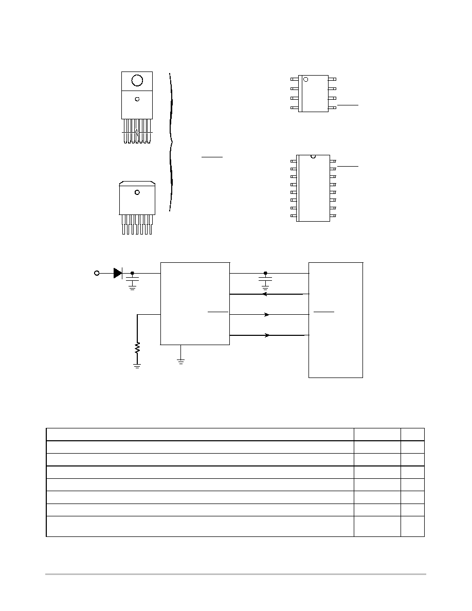
PIN CONNECTIONS
RESET
V
OUT
1
8
WAKE UP
Sense
WDI
GND
V
IN
Delay
V
IN
V
OUT
1
16
NC
Sense
WDI
NC
GND
GND
GND
GND
WAKE UP
NC
RESET
NC
Delay
NC
Pin 1. V
OUT
2. V
IN
3. WDI
4. GND
5. WAKE UP
6. RESET
7. Delay
SO≠16L
SO≠8
1
D
2
PAK
7≠PIN
TO≠220
SEVEN LEAD
1
C1*
V
OUT
GND
V
IN
WDI
NCV85085
1.0
µ
F
I/O
*
.
I/O
RESET
RESET
0.1
µ
F
C2
Microprocessor
Delay
R
Delay
120 k
V
BAT
*C1 required if regulator is located far from power supply filter.
V
DD
WAKE UP
Figure 1. Application Circuit
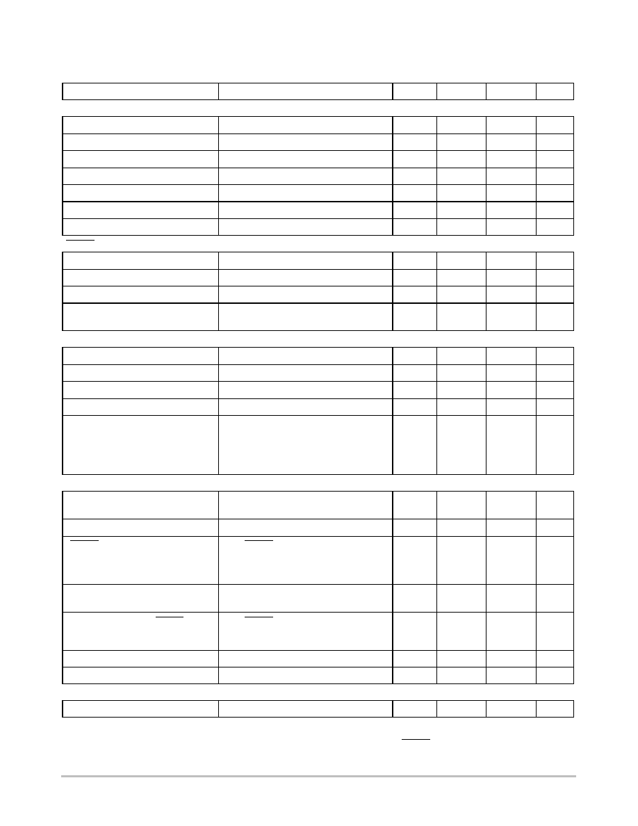
ABSOLUTE MAXIMUM RATINGS*
Rating
Value
Unit
Input Voltage, V
IN
≠0.3 to 45
V
Output Voltage, V
OUT
≠0.3 to 18
V
ESD Susceptibility (Human Body Model)
2.0
kV
Logic Inputs/Outputs (Reset, WDI, Wakeup)
≠0.3 to +7.0
V
Operating Junction Temperature, T
J
≠40 to150
∞
C
Storage Temperature Range, T
S
≠55 to +150
∞
C
Lead Temperature Soldering:
Wave Solder (through hole styles only) (Note 1.)
Reflow: (SMD styles only) (Note 2.)
260 peak
230 peak
∞
C
1. 10 second maximum.
2. 60 second maximum above 183
∞
C.
*The maximum package power dissipation must be observed.
NCV85085
http://onsemi.com
3
ELECTRICAL CHARACTERISTICS
(≠40
∞
C
T
J
125
∞
C; 6.0
V
V
IN
28 V, 100
µ
A
I
OUT
150 mA, C
2
= 1.0
µ
F,
R
Delay
= 120 k; unless otherwise specified.)
Characteristic
Test Conditions
Min
Typ
Max
Unit
Output Selection
Output Voltage, V
OUT
≠
4.90
5.00
5.10
V
Dropout Voltage (V
IN
≠ V
OUT
)
I
OUT
= 150 mA. Note 3.
≠
250
500
mV
Load Regulation
V
IN
= 14 V, 5.0 mA < I
OUT
< 150 mA
≠
5.0
30
mV
Line Regulation
I
OUT
= 5.0 mA
≠
5.0
20
mV
Current Limit
≠
250
400
≠
mA
Thermal Shutdown
Guaranteed by Design
150
180
210
∞
C
Quiescent Current
V
IN
= 12 V, I
OUT
= 250 mA
≠
100
150
µ
A
RESET
Threshold
≠
4.50
4.65
4.80
V
Output Low
R
LOAD
= 10 k to V
OUT
, V
OUT
1.0 V
≠
0.2
0.4
V
Output High
R
LOAD
= 10 k to GND
≠
V
OUT
≠ 0.2
V
OUT
≠ 0.4
V
Delay Time
R
Delay
= 60 k
3.0
1.5
5.0
2.5
7.0
3.5
ms
Watchdog Input
Threshold High
≠
70
≠
≠
%V
OUT
Threshold Low
≠
≠
≠
30
%V
OUT
Hysteresis
≠
25
100
≠
mV
Input Current
0 < WDI < 6.0 V
≠10
0
+10
µ
A
Pulse Width
50% WDI falling edge to
50% WDI rising edge and
50% WDI rising edge to
50% WDI falling edge
(see Figure 5)
5.0
≠
≠
µ
s
Wake Up Output
Wake Up Period
See Figures 4 and 5.
R
DELAY
= 60 k
32
16
40
20
48
24
ms
ms
Wake Up Duty Cycle Nominal
See Figure 3.
45
50
55
%
RESET HIGH to
Wake Up Rising Delay Time
50% RESET rising edge to
50% Wake Up edge
(see Figures 3 and 4)
R
DELAY
= 60 k
16
8
20
10
24
12
ms
ms
Wake Up Response to
Watchdog Input
50% WDI falling edge to
50% Wake Up falling edge
≠
2.0
10
µ
s
Wake Up Response to RESET
50% RESET falling edge to
50% Wake Up falling edge.
V
OUT
= 5.0 V
4.5 V
≠
2.0
10
µ
s
Output Low
R
LOAD
= 10 k
≠
0.2
0.4
V
Output High
R
LOAD
= 10 k
≠
V
OUT
≠ 0.2
V
OUT
≠ 0.4
Delay
Output Voltage
I
DELAY
= 50
µ
A. Note 4.
≠
1.25
≠
V
3. Measured when the output voltage has dropped 100 mV from the nominal value.
4. Current drain on the Delay pin directly affects the Delay Time, Wake Up Period, and the RESET to Wake Up Delay Time.
NCV85085
http://onsemi.com
4
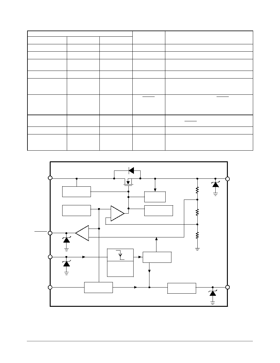
PACKAGE PIN DESCRIPTION
PACKAGE PIN #
TO≠220 & D
2
PAK
SO≠16L
SO≠8
PIN SYMBOL
FUNCTION
1
8
4
V
OUT
Regulated output voltage 5.0 V
±
2.0%.
2
9
5
V
IN
Supply Voltage to the IC.
3
11
6
WDI
CMOS compatible input lead. The watchdog func-
tion monitors the falling edge of the incoming signal.
4
4, 5, 12, 13
2
GND
Ground connection.
5
14
7
WAKE UP
CMOS compatible output consisting of a continu-
ously generated signal used to Wake Up the micro-
processor from sleep mode.
6
15
8
RESET
CMOS compatible output lead RESET goes low
whenever V
OUT
drops by more than 7.0% from
nominal, or during the absence of a correct watch-
dog signal.
7
16
1
Delay
Buffered bandgap voltage used to create timing
current for RESET and Wake Up from R
Delay.
≠
1, 2, 3, 6, 10
≠
NC
No Connection.
≠
7
3
Sense
Kelvin connection which allows remote sensing of
the output voltage for improved regulation. Connect
to V
OUT
if remote sensing is not required.
-
+
+
-
WAKE UP
Circuit
Timing
Circuit
Falling
Edge
Detect
Watchdog
Circuit
Thermal
Shutdown
Current
Limit
Charge
Pump
Bandgap
Reference
V
IN
RESET
V
OUT
Wake Up
WDI
Delay
Figure 2. Block Diagram
NCV85085
http://onsemi.com
5
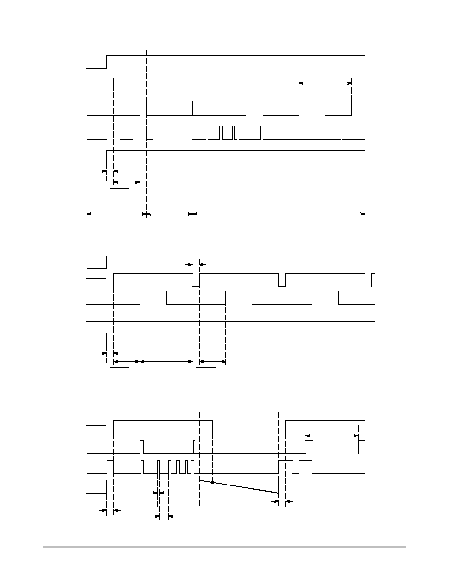
TIMING DIAGRAMS
Watchdog
Pulse Width
V
IN
RESET
Wake Up
WDI
V
OUT
Wake Up
Duty Cycle = 50%
Power Up
Sleep Mode
Normal Operation with Varying Watchdog Signal
RESET High
to Wake Up
Delay Time
POR
Figure 3. Power Up, Sleep Mode and Normal Operation
Figure 4. Error Condition: Watchdog Remains Low and a RESET Is Issued
V
IN
RESET
Wake Up
WDI
V
OUT
POR
RESET High
to Wake Up
Delay Time
RESET Delay Time
RESET High
to Wake Up
Delay Time
Wake Up
Period
POR
RESET
Wake Up
WDI
V
OUT
Watchdog Pulse Width
RESET Threshold
POR
Power Down
Wake Up Period
Figure 5. Power Down and Restart Sequence