
©
Semiconductor Components Industries, LLC, 2003
September, 2003 - Rev. 10
1
Publication Order Number:
NCV8800/D
NCV8800 Series
Synchronous Buck Regulator
with 1.0 Amp Switch
The NCV8800 is an automotive synchronous step-down buck
regulator. This part provides an efficient step-down voltage compared
to linear regulators. The NCV8800 uses very few external components
allowing for maximum use of printed circuit board space.
Features
∑
Output Voltage Options: 2.6 V, 3.3 V, 5.0 V, 7.5 V
∑
±
3.0% Output
∑
3.5 V Operation
∑
AUXILIARY Hold Up Pin (for Cranking Conditions)
∑
On-Chip Switching Power Devices (0.4
R
DS(ON)
)
∑
Constant Frequency
∑
Synchronous Operation
∑
On-Chip Charge Pump Control Circuitry
∑
Nonoverlap Logic
∑
Power Up Sequencing Control Option (2.6 V and 3.3 V Only)
∑
ENABLE Battery Voltage Capable Option
∑
Selectable Reset Delay
∑
Dual Pin Feedback Connection
∑
V
2
TM
Control Topology
∑
Internally Fused Leads in SO-16L Package
∑
NCV Prefix for Automotive and Other Applications Requiring Site
and Change Control
Typical Applications
∑
Telecommunications
∑
Mobile Multimedia
∑
Instrumentation
∑
Automotive Entertainment Systems
10
20
30
40
50
60
70
80
90
100
0
100
200
300
400
500
600
700
800
LOAD CURRENT (mA)
EFFICIENCY
(%)
Figure 1. Efficiency vs. Load Current
V
OUT
= 7.5 V
V
OUT
= 5.0 V
V
OUT
= 3.3 V
V
OUT
= 2.6 V
V
IN
= 13.5 V
L =100
m
H
0
SO-16L
DW SUFFIX
CASE 751G
1
16
NCV8800xy
A
W
L
YYWW
COMP
FB2
1
16
NC
FB1
V
IN2
DELAY
GND
GND
GND
GND
SWITCH
RESET
CP
ENABLE
V
IN
AUXILIARY
PIN CONNECTIONS AND
MARKING DIAGRAM
x
= Voltage Ratings as Indicated Below:
2 = 2.6 V
3 = 3.3 V
5 = 5.0 V
7 = 7.5 V
y
= ENABLE Option as Indicated Below:
S = Sequenced
H = High Voltage
A
= Assembly Location
WL, L
= Wafer Lot
YY, Y
= Year
WW, W = Work Week
See detailed ordering and shipping information in the package
dimensions section on page 11 of this data sheet.
ORDERING INFORMATION
http://onsemi.com

NCV8800 Series
http://onsemi.com
2
Figure 2. Application Diagram
AUXILIARY
ENABLE
RESET
GND
GND
DELAY
FB1
FB2
V
IN
CP
SWITCH
GND
GND
V
IN2
NC
COMP
NCV8800
5.1 k
RESET
0.1
µ
F
100
µ
F
100
µ
H
0.01
µ
F
V
BAT
V
OUT
External Regulator
Auxiliary Supply
(optional)
0.1
µ
F
1.0 k
10
µ
F*
*The supply capacitor
must be located
physically close to
the IC pins.
100
0.01
µ
F
MRA4004T3
Figure 3. Typical Operation With An 8.0
W
Load

NCV8800 Series
http://onsemi.com
3
MAXIMUM RATINGS*
Rating
Value
Unit
Supply Voltages, V
IN
, V
IN2
-0.3 to 45
V
AUXILIARY
-0.3 to 8.0
V
ENABLE (Sequenced Option)
-0.3 to 7.0
V
ENABLE (High Voltage Option)
-0.3 to 8.0
V
RESET
-0.3 to 30
V
DELAY
-0.3 to 7.0
V
SWITCH (V
5VSENSE
= 0 V)
-1.0 to 45
V
Operating Junction Temperature
-40 to 150
∞
C
Storage Temperature Range
-55 to 150
∞
C
ESD - Human Body Model (AUXILIARY, ENABLE, RESET, DELAY, FB1, FB2, CP, SWITCH, COMP)
Human Body Model (VIN, VIN2)
Machine Model (All Pins)
2.0
1.3
200
kV
kV
V
Package Thermal Resistance, SO-16L
Junction-to-Case, R
q
JC
Junction-to-Ambient, R
q
JA
18
80
∞
C/W
Lead Temperature Soldering:
Reflow (SMD Style Only) (Note 1)
240 Peak
(Note 2)
∞
C
1. 60 second maximum above 183
∞
C.
2. -5
∞
C/+0
∞
C allowable condition.
*The maximum package power dissipation must be observed.

NCV8800 Series
http://onsemi.com
4
ELECTRICAL CHARACTERISTICS
(-40
∞
C
T
J
125
∞
C; Sequenced ENABLE Option: 3.5 V
V
IN
16 V,
3.5 V
V
IN2
16 V, AUXILIARY = 6.0 V, ENABLE = 5.0 V; High Voltage ENABLE Option: 6.0 V
V
IN
16 V, 6.0 V
V
IN2
16 V;
unless otherwise stated.)
Characteristic
Test Conditions
Min
Typ
Max
Unit
General
Quiescent Current (V
IN2
)
Sleep Mode
Operating
ENABLE = 0 V, V
IN
= 12.6 V,
T
J
= -40
∞
C
ENABLE = 0 V, V
IN
= 12.6 V,
T
J
= 25
∞
C, 125
∞
C
ENABLE = 5.0 V, V
IN
= 13.5 V, I
OUT
= 0
-
-
-
-
-
-
40
30
15
µ
A
µ
A
mA
Switching Frequency
-
180
200
230
kHz
Switching Duty Cycle
-
85
90
95
%
Thermal Shutdown
Note 3
150
165
200
∞
C
Feedback
Feedback Voltage Threshold, 2.6 V Option (V
FB
)
-
2.522
2.6
2.678
V
Feedback Voltage Threshold, 3.3 V Option (V
FB
)
-
3.201
3.3
3.399
V
Feedback Voltage Threshold, 5.0 V Option (V
FB
)
-
4.850
5.0
5.150
V
Feedback Voltage Threshold, 7.5 V Option (V
FB
)
-
7.275
7.5
7.725
V
RESET
Undervoltage RESET Threshold, 2.6 V Option
V
OUT
Increasing
V
OUT
Decreasing
2.44
2.40
-
-
V
FB
V
FB
- 0.04
V
V
Undervoltage RESET Hysteresis, 2.6 V Option
-
40
-
-
mV
Overvoltage RESET Threshold, 2.6 V Option
V
OUT
Increasing
V
OUT
Decreasing
V
FB
+ 0.04
V
FB
-
-
2.80
2.76
V
V
Overvoltage RESET Hysteresis, 2.6 V Option
-
40
-
-
mV
Undervoltage RESET Threshold, 3.3 V Option
V
OUT
Increasing
V
OUT
Decreasing
3.10
3.04
-
-
V
FB
V
FB
- 0.05
V
V
Undervoltage RESET Hysteresis, 3.3 V Option
-
50
-
-
mV
Overvoltage RESET Threshold, 3.3 V Option
V
OUT
Increasing
V
OUT
Decreasing
V
FB
+ 0.05
V
FB
-
-
3.56
3.51
V
V
Overvoltage RESET Hysteresis, 3.3 V Option
-
50
-
-
mV
Undervoltage RESET Threshold, 5.0 V Option
V
OUT
Increasing
V
OUT
Decreasing
4.70
4.61
-
-
V
FB
V
FB
- 0.075
V
V
Undervoltage RESET Hysteresis, 5.0 V Option
-
75
-
-
mV
Overvoltage RESET Threshold, 5.0 V Option
V
OUT
Increasing
V
OUT
Decreasing
V
FB
+ 0.075
V
FB
-
-
5.39
5.31
V
V
Overvoltage RESET Hysteresis, 5.0 V Option
-
75
-
-
mV
Undervoltage RESET Threshold, 7.5 V Option
V
OUT
Increasing
V
OUT
Decreasing
7.05
6.92
-
-
V
FB
V
FB
- 0.115
V
V
Undervoltage RESET Hysteresis, 7.5 V Option
-
115
-
-
mV
Overvoltage RESET Threshold, 7.5 V Option
V
OUT
Increasing
V
OUT
Decreasing
V
FB
+ 0.115
V
FB
-
-
8.08
7.96
V
V
Overvoltage RESET Hysteresis, 7.5 V Option
-
115
-
-
mV
3. Guaranteed By Design.
NCV8800 Series
http://onsemi.com
5
ELECTRICAL CHARACTERISTICS (continued)
(-40
∞
C
T
J
125
∞
C; Sequenced ENABLE Option: 3.5 V
V
IN
16 V,
3.5 V
V
IN2
16 V, AUXILIARY = 6.0 V, ENABLE = 5.0 V; High Voltage ENABLE Option: 6.0 V
V
IN
16 V, 6.0 V
V
IN2
16 V;
unless otherwise stated.)
Characteristic
Test Conditions
Min
Typ
Max
Unit
RESET
RESET Leakage Current
RESET = 5.25 V
-
-
25
µ
A
RESET Output Low Voltage
I
OUT
= 1.6 mA
-
-
0.4
V
RESET Delay
DELAY Connected to FB1, FB2
DELAY = 0 V
28.70
14.35
32.60
16.30
36.66
18.33
ms
ms
ENABLE
ENABLE Threshold
Increasing
Decreasing
1.1
1.0
1.9
1.6
2.3
2.2
V
V
ENABLE Hysteresis
-
100
250
550
mV
ENABLE Input Resistance
ENABLE = 5.25 V, V
IN2
= 13.5 V
50
100
200
k
W
DELAY
DELAY Input Current
DELAY = 5.15 V
4.0
10
16
µ
A
SWITCH
SWITCH ON Resistance
I
SWITCH
= 0.5 A, T
J
= -40
∞
C, 25
∞
C
I
SWITCH
= 0.5 A, T
J
= 125
∞
C
-
-
0.40
0.55
0.60
0.75
Current Limit
-
1.0
1.6
2.5
A
Error Amplifier
Error Amplifier Transconductance
2.6 V Option
3.3 V Option
5.0 V Option
7.5 V Option
2.58 V
FB1
2.62 V
2.58 V
FB2
2.62 V
3.275 V
FB1
3.325 V
3.275 V
FB2
3.325 V
4.962 V
FB1
5.038 V
4.962 V
FB2
5.038 V
7.442 V
FB1
7.558 V
7.442 V
FB2
7.558 V
0.55
0.43
0.28
0.19
-
-
-
-
2.10
1.65
1.09
0.73
1/m
Error Amplifier Bandwidth
Note 4
1.0
-
-
MHz
Output Tracking (Sequencing)
Feedback to ENABLE Tracking Voltage, 2.6 V Option
-
60
67
75
%
Feedback to ENABLE Tracking Voltage, 3.3 V Option
-
80
85
90
%
4. Guaranteed By Design.

NCV8800 Series
http://onsemi.com
6
PACKAGE PIN DESCRIPTION
PACKAGE LEAD #
LEAD SYMBOL
FUNCTION
1
AUXILIARY
Alternate path for voltage input to the IC.
2
ENABLE
Sense for powerup. This pin must be high before SWITCH turns on.
3
RESET
CMOS compatible open drain output lead. RESET goes low whenever FB1 or FB2 is
below the RESET low threshold, or above the RESET high threshold.
4, 5, 12, 13
GND
Ground.
6
DELAY
RESET delay control. Time is doubled when pin moved to FB1 or FB2 from 0 V.
7
FB1
Voltage feedback to error amplifier. Shorted with FB2.
8
FB2
Voltage feedback to error amplifier. Shorted with FB1.
9
COMP
Loop compensation node for error amplifier. (1.0 k
and 0.1
µ
F to ground).
10
NC
No connection.
11
V
IN2
Supply input voltage for internal bias circuitry.
14
SWITCH
Drive for external inductor.
15
CP
Node for charge pump bootstrap capacitor.
16
V
IN
Supply input voltage for output drivers.

NCV8800
Series
http://onsemi.com
7
Figure 4. Block Diagram
Nonoverlap
Logic and Drive
R
S
Q
Q
LATCH
0.4
0.4
SWITCH
OVLO
Current Limit
GND
UVLO
200 kHz
OSC
ART Ramp
+
Error Amp
POR
Timer
-
-
+
-
+
RESET
CP Control
V
IN
Bandgap
Voltage
Reference
5.1 k
33
µ
H
2.6 V
V
BAT
0.01
µ
F
CP
Over/Under
Voltage
RESET COMP
Power Up/Down
Sequence
and ENABLE
OVLO
UVLO
DELAY
COMP
ENABLE
AUXILIARY
FB1
FB2
PWM COMP
Current Limit
100
µ
F
V
IN2
BIAS
Thermal Shutdown
0.1
m
F
100
W
MRA4004T3
1 k
0.1
m
F

NCV8800 Series
http://onsemi.com
8
CIRCUIT DESCRIPTION
ENABLE
The NCV8800 remains in sleep mode drawing less than
25
µ
A of quiescent current until the ENABLE pin is brought
high powering up the device. There are two options
available for the ENABLE feature.
∑
Option 1 (Sequenced). The output voltage tracks the
ENABLE pin with a maximum delta voltage between
them (reference the Output Tracking specs in the
Electrical Characteristics). This allows the device to be
used with microprocessors requiring dual supply
voltages. One voltage is typically needed to power the
core of the microprocessor, and another high voltage is
needed to power the microprocessor I/O.
∑
Option 2 (High Voltage). This option removes the
sequencing feature above, and allows the device to be
controlled up to the battery voltage on the ENABLE
pin with an external resistor (10 k). See Figure 5.
Figure 5. Switched Battery Application
ENABLE
V
IN
V
BAT
10 k
AUXILIARY
The AUXILIARY pin provides an alternate path for the IC
to maintain operation. The AUXILIARY pin is diode OR'd
with the V
IN
pin to the control circuitry (the DMOS output
drivers are not included). If the voltage (V
IN
) from the
battery dips as low as 3.5 V during a crank condition, the
NCV8800 will maintain operation through a 6.0 V(min)
connection on the AUXILIARY pin. Using this feature is
optional. This pin should be grounded when not in use.
V
IN
Normal supply voltage input. An external diode must be
provided to afford reverse battery protection.
SWITCH
DMOS output drivers with 0.75
max push/pull
capability. Non-overlap logic is provided to guarantee shoot
through current is minimized.
RESET
The RESET is an open drain output which goes low when
the feedback voltage on FB1 and FB2 goes below the
undervoltage RESET threshold. The output also goes low
when the voltage on FB1 and FB2 exceeds the overvoltage
RESET threshold. The RESET output is an open drain
output capable of sinking 1.6 mA.
FB1 and FB2
FB1 and FB2 are the feedback pins to the error amplifier,
which control the output SWITCH as needed to the
regulated output. They are internally wire bonded to the
same electrical connection providing double protection for
an open circuit which would cause the buck regulator to rise
above its desired output reaching the voltage on V
IN
. These
pins also provide the feedback path for the RESET function.
DELAY
There are two options for the delay time for the RESET to go
low. Connecting the pin to GND will provide a minimum of 14
ms. Connecting the pin to FB1 and FB2 will provide a
minimum of 28 ms. Absolute max voltage on the DELAY
pin is 7.0 V. Use a resistor divider to run off higher voltages.
The 7.5 V option will require this divider (see Figure 6).
Figure 6.
DELAY
(7.0 V max)
V
OUT
COMP
The COMP pin provides access to the error amplifiers
output. Switching power supplies work as feedback control
systems, and require compensation for stability. A 1.0 k
resistor and 0.1
µ
F capacitor work well in the application in
Figure 2.
CP
The on-chip DMOS drivers require the gates of the
devices to be pulled above their drain voltage. An external
capacitor located between the SWITCH output, and the CP
pin provides the charge pump action to drive the gate of the
high-side driver high enough to turn the device on.

NCV8800 Series
http://onsemi.com
9
APPLICATIONS INFORMATION
V
OUT
NCV8800
Switch
FB2
R
EX
Power Up/Down
Sequence and
ENABLE
-
+
R2
21.4 k
Error Amp
1.20 V
56
µ
A
FB1
R1*
Figure 7.
*The value of R1
is dependent
on the output
voltage option
and is between
25 k and 200 k.
Increasing the Output Voltage
Adjustments to the output voltage can be made with an
external resistor (R
EX
). The increase in output voltage will
typically be 56
µ
A
◊
R
EX
. Caution and consideration must
be given to the tracking feature and temperature coefficient
and matching of internal and external resistors. Output
tracking always follows the Feedback pins (FB1 and FB2).
The typical temperature coefficient for R1 and R2 is
+4600 ppm/
∞
C.
THEORY OF OPERATION
V
2
Control Method
The V
2
method of control uses a ramp signal that is
generated by the ESR of the output capacitors. This ramp is
proportional to the AC current through the main inductor
and is offset by the value of the DC output voltage. This
control scheme inherently compensates for variations in
either line or load conditions, since the ramp signal is
generated from the output voltage itself. This control
scheme differs from traditional techniques such as voltage
mode, which generates an artificial ramp, and current mode,
which generates a ramp from inductor current.
-
+
-
+
Ramp Signal
Error Signal
Error Amplifier
COMP
GATE(L)
GATE(H)
Output
Voltage
Feedback
PWM Comparator
Figure 8. V
2
Control Block Diagram
Reference
Voltage
The V
2
control method is illustrated in Figure 8. The output
voltage is used to generate both the error signal and the ramp
signal. Since the ramp signal is simply the output voltage, it
is affected by any change in the output regardless of the origin
of the change. The ramp signal also contains the DC portion
of the output voltage, which allows the control circuit to drive
the main switch to 0% or 100% duty cycle as required.
A change in line voltage changes the current ramp in the
inductor, affecting the ramp signal, which causes the V
2
control scheme to compensate the duty cycle. Since the
change in the inductor current modifies the ramp signal, as
in current mode control, the V
2
control scheme has the same
advantages in line transient response.
A change in load current will have an effect on the output
voltage, altering the ramp signal. A load step immediately
changes the state of the comparator output, which controls
the main switch. Load transient response is determined only
by the comparator response time and the transition speed of
the main switch. The reaction time to an output load step has
no relation to the crossover frequency of the error signal
loop, as in traditional control methods.
The error signal loop can have a low crossover frequency,
since transient response is handled by the ramp signal loop.
The main purpose of this "slow" feedback loop is to provide
DC accuracy. Noise immunity is significantly improved,
since the error amplifier bandwidth can be rolled off at a low
frequency. Enhanced noise immunity improves remote
sensing of the output voltage, since the noise associated with
long feedback traces can be effectively filtered.
Line and load regulations are drastically improved
because there are two independent voltage loops. A voltage
mode controller relies on a change in the error signal to
compensate for a derivation in either line or load voltage.
This change in the error signal causes the output voltage to
change corresponding to the gain of the error amplifier,
which is normally specified as line and load regulation. A
current mode controller maintains fixed error signal under
deviation in the line voltage, since the slope of the ramp
signal changes, but still relies on a change in the error signal
for a deviation in load. The V
2
method of control maintains
a fixed error signal for both line and load variations, since
both line and load affect the ramp signal.
Constant Frequency Operation
During normal operation, the oscillator generates a 200 kHz,
90% duty cycle waveform. The rising edge of this waveform
determines the beginning of each switching cycle, at which
point the high-side switch will be turned on. The high-side
switch will be turned off when the ramp signal intersects the
output of the error amplifier (COMP pin voltage).
Therefore,
the switch duty cycle can be modified to regulate
the output voltage to the desired value as line and load
conditions change.

NCV8800 Series
http://onsemi.com
10
The major advantage of constant frequency operation is
that the component selections, especially the magnetic
component design, become very easy. Oscillator frequency
is fixed at 200 kHz.
Start-Up
After the NCV8800 is powered up, the error amplifier will
begin linearly charging the COMP pin capacitor. The COMP
capacitance and the source current of the error amplifier
determine the slew rate of COMP voltage. The output of the
error amplifier is connected internally to the inverting input
of the PWM comparator and it is compared with the divided
down output voltage FB1/FB2 at the non-inverting input of
the PWM comparator. At the beginning of each switching
cycle, the oscillator output will set the PWM latch. This
causes the high-side switch to turn on and the regulator
output voltage to ramp up.
When the divided down output voltage achieves a level set
by the COMP voltage, the high-side switch will be turned
off. The V
2
control loop will adjust the high-side switch
duty cycle as required to ensure the regulator output voltage
tracks the COMP voltage. Since the COMP voltage
increases gradually, Soft Start can be achieved.
Overcurrent Protection
The output switch is protected on both the high side and
low side. Current limit is set at 1.0 A (min).
Figure 9. 16 Lead SOW (4 Leads Fused),
q
JA as
a Function of the Pad Copper Area (2 oz. Cu.
Thickness), Board Material = 0.0625
,
G-10/R-4
40
70
90
100
Thermal
Resistance,
Junction to Ambient, R
q
JA
, (
∞
C/W)
0
Copper Area (inch
2
)
0.5
1.0
1.5
2.0
3.0
80
60
50
2.5
Heat Sinks
A heat sink effectively increases the surface area of the
package to improve the flow of heat away from the IC and
into the surrounding air.
Each material in the heat flow path between the IC and the
outside environment will have a thermal resistance. Like
series electrical resistances, these resistances are summed to
determine the value of R
qJA
:
R
q
JA
+
R
q
JC
)
R
q
CS
)
R
q
SA
(3)
where:
R
qJC
= the junction-to-case thermal resistance,
R
qCS
= the case-to-heatsink thermal resistance, and
R
qSA
= the heatsink-to-ambient thermal resistance.
R
qJC
appears in the package section of the data sheet. Like
R
qJA
, it too is a function of package type. R
qCS
and R
qSA
are
functions of the package type, heatsink and the interface
between them. These values appear in heat sink data sheets
of heat sink manufacturers.
NCV8800 Series
http://onsemi.com
11
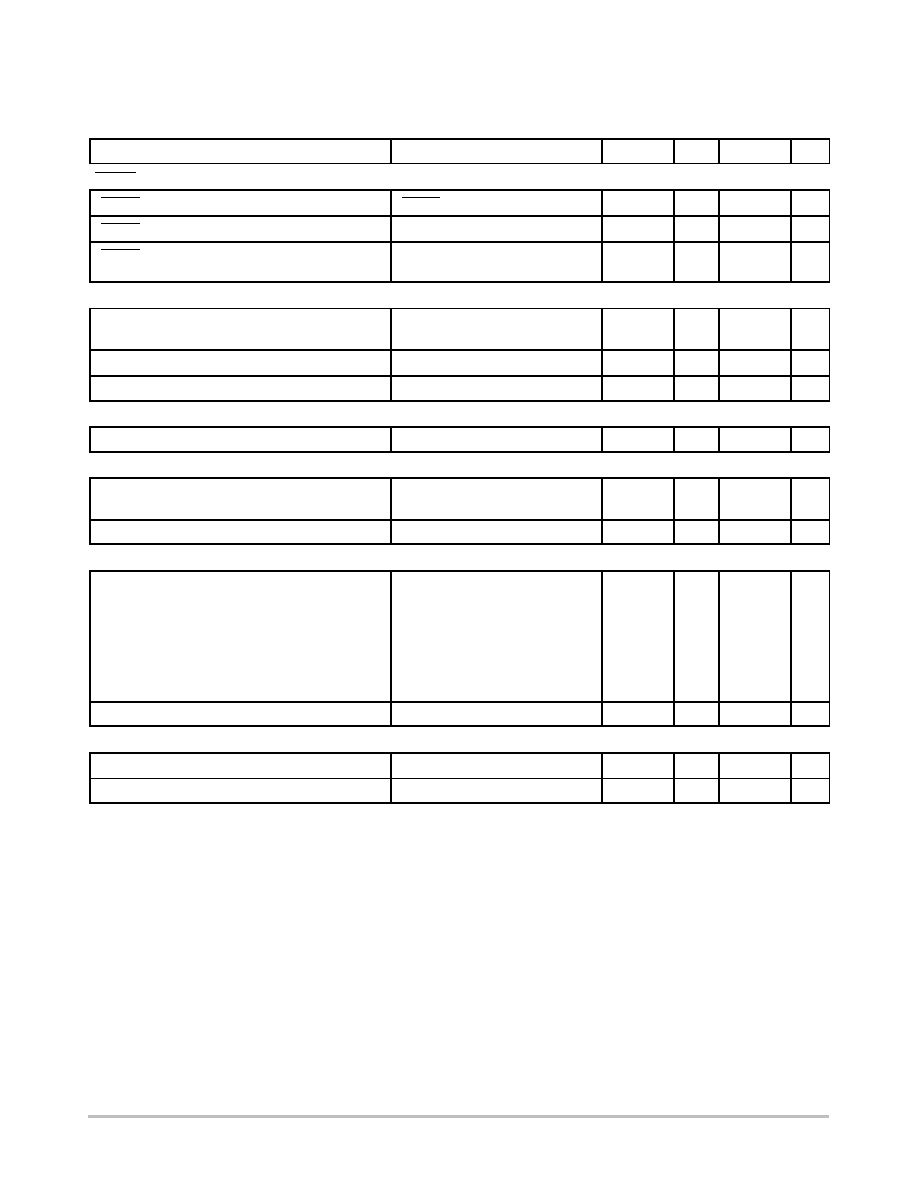
ORDERING INFORMATION
Device
Output Voltage
ENABLE Option
Package
Shipping
NCV8800SDW26
Sequenced
46 Units/Rail
NCV8800SDW26R2
2 6 V
Sequenced
1000 Tape & Reel
NCV8800HDW26
2.6 V
High Voltage
46 Units/Rail
NCV8800HDW26R2
High Voltage
1000 Tape & Reel
NCV8800SDW33
Sequenced
46 Units/Rail
NCV8800SDW33R2
3 3 V
Sequenced
SO 16L
1000 Tape & Reel
NCV8800HDW33
3.3 V
High Voltage
SO-16L
46 Units/Rail
NCV8800HDW33R2
High Voltage
1000 Tape & Reel
NCV8800HDW50
5 0 V
46 Units/Rail
NCV8800HDW50R2
5.0 V
High Voltage
1000 Tape & Reel
NCV8800HDW75
7 5 V
High Voltage
46 Units/Rail
NCV8800HDW75R2
7.5 V
1000 Tape & Reel
For information on tape and reel specifications, including part orientation and tape sizes, please refer to our Tape and Reel Packaging
Specifications Brochure, BRD8011/D.

NCV8800 Series
http://onsemi.com
12
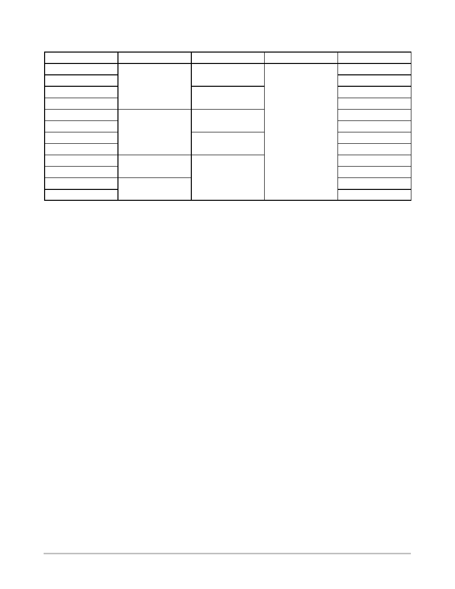
PACKAGE DIMENSIONS
SO-16L
DW SUFFIX
CASE 751G-03
ISSUE B
D
14X
B
16X
SEATING
PLANE
S
A
M
0.25
B
S
T
16
9
8
1
h
X 45
_
M
B
M
0.25
H
8X
E
B
A
e
T
A1
A
L
C
q
NOTES:
1. DIMENSIONS ARE IN MILLIMETERS.
2. INTERPRET DIMENSIONS AND TOLERANCES
PER ASME Y14.5M, 1994.
3. DIMENSIONS D AND E DO NOT INLCUDE MOLD
PROTRUSION.
4. MAXIMUM MOLD PROTRUSION 0.15 PER SIDE.
5. DIMENSION B DOES NOT INCLUDE DAMBAR
PROTRUSION. ALLOWABLE DAMBAR
PROTRUSION SHALL BE 0.13 TOTAL IN EXCESS
OF THE B DIMENSION AT MAXIMUM MATERIAL
CONDITION.
DIM
MIN
MAX
MILLIMETERS
A
2.35
2.65
A1
0.10
0.25
B
0.35
0.49
C
0.23
0.32
D
10.15
10.45
E
7.40
7.60
e
1.27 BSC
H
10.05
10.55
h
0.25
0.75
L
0.50
0.90
q
0
7
_
_
ON Semiconductor and are registered trademarks of Semiconductor Components Industries, LLC (SCILLC). SCILLC reserves the right to make
changes without further notice to any products herein. SCILLC makes no warranty, representation or guarantee regarding the suitability of its products for any
particular purpose, nor does SCILLC assume any liability arising out of the application or use of any product or circuit, and specifically disclaims any and all
liability, including without limitation special, consequential or incidental damages. "Typical" parameters which may be provided in SCILLC data sheets and/or
specifications can and do vary in different applications and actual performance may vary over time. All operating parameters, including "Typicals" must be
validated for each customer application by customer's technical experts. SCILLC does not convey any license under its patent rights nor the rights of others.
SCILLC products are not designed, intended, or authorized for use as components in systems intended for surgical implant into the body, or other applications
intended to support or sustain life, or for any other application in which the failure of the SCILLC product could create a situation where personal injury or death
may occur. Should Buyer purchase or use SCILLC products for any such unintended or unauthorized application, Buyer shall indemnify and hold SCILLC
and its officers, employees, subsidiaries, affiliates, and distributors harmless against all claims, costs, damages, and expenses, and reasonable attorney fees
arising out of, directly or indirectly, any claim of personal injury or death associated with such unintended or unauthorized use, even if such claim alleges that
SCILLC was negligent regarding the design or manufacture of the part. SCILLC is an Equal Opportunity/Affirmative Action Employer.
PUBLICATION ORDERING INFORMATION
JAPAN: ON Semiconductor, Japan Customer Focus Center
2-9-1 Kamimeguro, Meguro-ku, Tokyo, Japan 153-0051
Phone: 81-3-5773-3850
ON Semiconductor Website: http://onsemi.com
For additional information, please contact your local
Sales Representative.
NCV8800/D
V
2
is a trademark of Switch Power, Inc.
Literature Fulfillment:
Literature Distribution Center for ON Semiconductor
P.O. Box 5163, Denver, Colorado 80217 USA
Phone: 303-675-2175 or 800-344-3860 Toll Free USA/Canada
Fax: 303-675-2176 or 800-344-3867 Toll Free USA/Canada
Email: orderlit@onsemi.com
N. American Technical Support: 800-282-9855 Toll Free USA/Canada