 | –≠–ª–µ–∫—Ç—Ä–æ–Ω–Ω—ã–π –∫–æ–º–ø–æ–Ω–µ–Ω—Ç: NJL3281D | –°–∫–∞—á–∞—Ç—å:  PDF PDF  ZIP ZIP |
©
Semiconductor Components Industries, LLC, 2004
December, 2004 - Rev. P1
1
Publication Order Number:
NJL3281D/D
NJL3281D (NPN)
NJL1302D (PNP)
Product Preview
Complementary
ThermalTrak
TM
Transistors
The ThermalTrak family of devices has been designed to eliminate
thermal equilibrium lag time and bias trimming in audio amplifier
applications. They can also be used in other applications as transistor
die protection devices.
Features
∑
Thermally Matched Bias Diode
∑
Instant Thermal Bias Tracking
∑
Absolute Thermal Integrity
∑
High Safe Operating Area
Benefits
∑
Eliminates Thermal Equilibrium Lag Time and Bias Trimming
∑
Superior Sound Quality Through Improved Dynamic Temperature
Response
∑
Significantly Improved Bias Stability
∑
Simplified Assembly
Reduced Labor Costs
Reduced Component Count
∑
High Reliability
Applications
∑
High-End Consumer Audio Products
Home Amplifiers
Home Receivers
∑
Professional Audio Amplifiers
Theater and Stadium Sound Systems
Public Address Systems (PAs)
This document contains information on a product under development. ON Semiconductor
reserves the right to change or discontinue this product without notice.
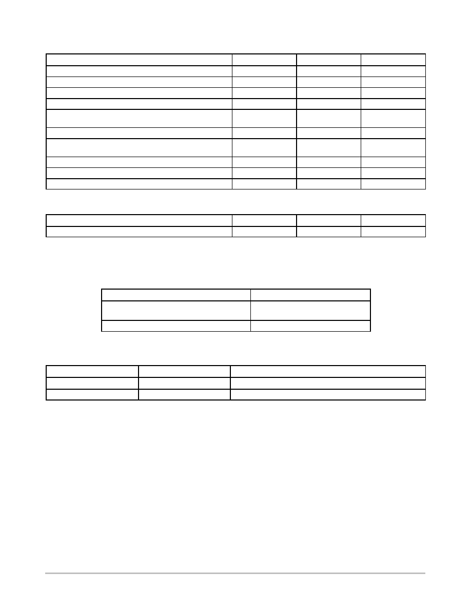
TO-264, 5 LEAD
CASE 340AA
STYLE 1
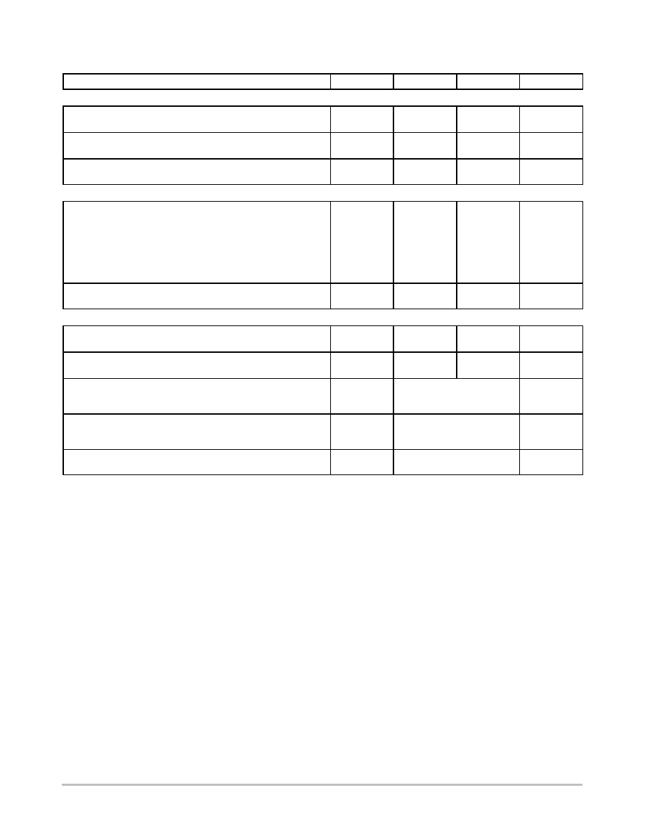
MARKING DIAGRAM
http://onsemi.com
xxxx
= Specific Device Code
A
= Assembly Location
YY
= Year
WW
= Work Week
NJLxxxxD
AYYWW
SCHEMATIC
BIPOLAR POWER
TRANSISTORS
15 A, 230 V, 200 W
See detailed ordering and shipping information in the package
dimensions section on page 2 of this data sheet.
ORDERING INFORMATION
NJL3281D (NPN) NJL1302D (PNP)
http://onsemi.com
2
MAXIMUM RATINGS
(T
J
= 25
∞
C unless otherwise noted)
Rating
Symbol
Value
Unit
Collector-Emitter Voltage
V
CEO
230
Vdc
Collector-Base Voltage
V
CBO
230
Vdc
Emitter-Base Voltage
V
EBO
5
Vdc
Collector-Emitter Voltage - 1.5 V
V
CEX
230
Vdc
Collector Current
- Continuous
- Peak (Note 1)
I
C
15
25
Adc
Base Current - Continuous
I
B
1.5
Adc
Total Power Dissipation @ T
C
= 25
∞
C
Derate Above 25
∞
C
P
D
200
1.43
W
W/
∞
C
Operating and Storage Junction Temperature Range
T
J
, T
stg
- 65 to +150
∞
C
DC Blocking Voltage
V
R
200
V
Average Rectified Forward Current
I
F(AV)
1.0
A
THERMAL CHARACTERISTICS
Characteristic
Symbol
Max
Unit
Thermal Resistance, Junction-to-Case
R
q
JC
0.625
∞
C/W
Maximum ratings are those values beyond which device damage can occur. Maximum ratings applied to the device are individual stress limit
values (not normal operating conditions) and are not valid simultaneously. If these limits are exceeded, device functional operation is not implied,
damage may occur and reliability may be affected.
1. Pulse Test: Pulse Width = 5 ms, Duty Cycle < 10%.
ATTRIBUTES
Characteristic
Value
ESD Protection
Human Body Model
Machine Model
>8000 V
> 400 V
Flammability Rating
UL 94 V-0 @ 0.125 in
ORDERING INFORMATION
Device
Package
Shipping
NJL3281D
TO-264
25 Units / Rail
NJL1302D
TO-264
25 Units / Rail
NJL3281D (NPN) NJL1302D (PNP)
http://onsemi.com
3
ELECTRICAL CHARACTERISTICS
(T
C
= 25
∞
C unless otherwise noted)
Characteristic
Symbol
Min
Max
Unit
OFF CHARACTERISTICS
Collector-Emitter Sustaining Voltage
(I
C
= 100 mAdc, I
B
= 0)
V
CEO(sus)
230
-
Vdc
Collector Cutoff Current
(V
CB
= 230 Vdc, I
E
= 0)
I
CBO
-
50
m
Adc
Emitter Cutoff Current
(V
EB
= 5 Vdc, I
C
= 0)
I
EBO
-
5
m
Adc
ON CHARACTERISTICS
DC Current Gain
(I
C
= 100 mAdc, V
CE
= 5 Vdc)
(I
C
= 1 Adc, V
CE
= 5 Vdc)
(I
C
= 3 Adc, V
CE
= 5 Vdc)
(I
C
= 5 Adc, V
CE
= 5 Vdc)
(I
C
= 7 Adc, V
CE
= 5 Vdc)
(I
C
= 8 Adc, V
CE
= 5 Vdc)
(I
C
= 15 Adc, V
CE
= 5 Vdc)
h
FE
60
60
60
60
60
45
12
175
175
175
175
175
-
-
Collector-Emitter Saturation Voltage
(I
C
= 10 Adc, I
B
= 1 Adc)
V
CE(sat)
-
3
Vdc
DYNAMIC CHARACTERISTICS
Current-Gain - Bandwidth Product
(I
C
= 1 Adc, V
CE
= 5 Vdc, f
test
= 1 MHz)
f
T
30
-
MHz
Output Capacitance
(V
CB
= 10 Vdc, I
E
= 0, f
test
= 1
MHz)
C
ob
-
600
pF
Maximum Instantaneous Forward Voltage (Note 2)
(i
F
= 1.0 A, T
J
= 25
∞
C)
(i
F
= 1.0 A, T
J
= 150
∞
C)
v
F
1.0
0.83
V
Maximum Instantaneous Reverse Current (Note 2)
(Rated dc Voltage, T
J
= 25
∞
C)
(Rated dc Voltage, T
J
= 150
∞
C)
i
R
10
100
m
A
Maximum Reverse Recovery Time
(i
F
= 1.0 A, di/dt = 50 A/
m
s)
t
rr
100
ns
2. Pulse Test: Pulse Width = 300
m
s, Duty Cycle
v
2.0%.
NJL3281D (NPN) NJL1302D (PNP)
http://onsemi.com
4
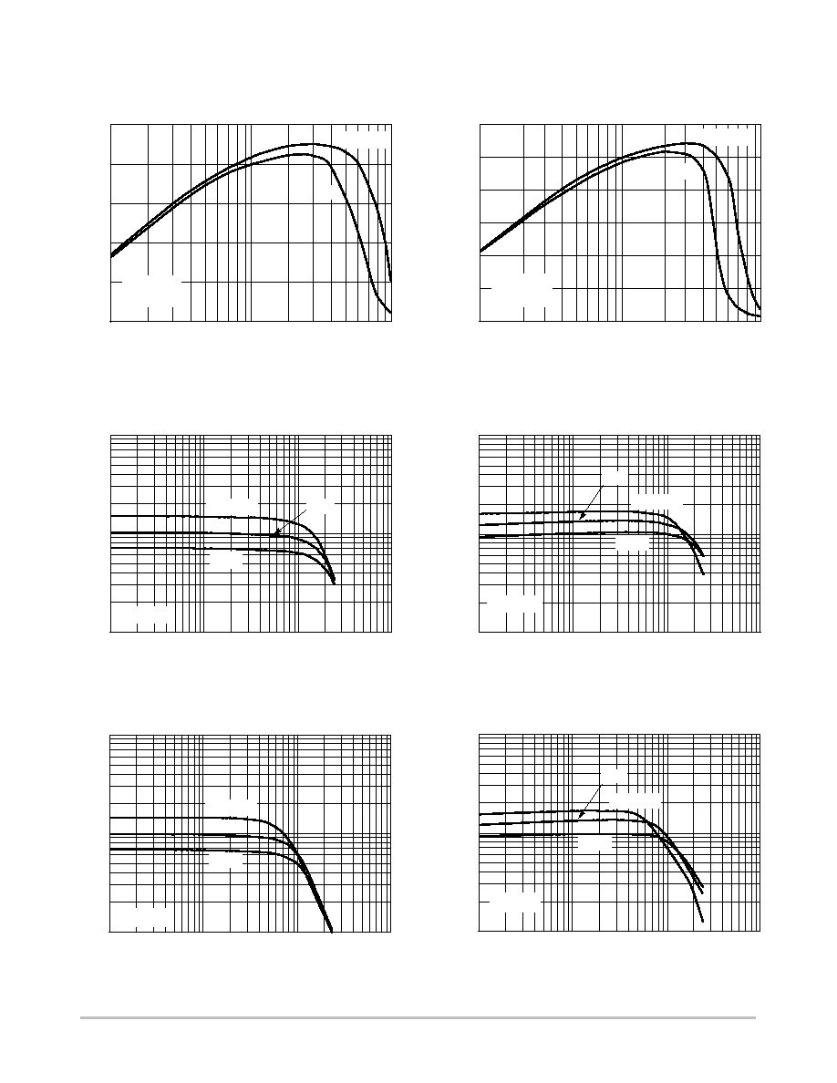
I
C
, COLLECTOR CURRENT (AMPS)
Figure 1. Typical Current Gain
Bandwidth Product
Figure 2. Typical Current Gain
Bandwidth Product
f, CURRENT
BANDWIDTH PRODUCT
(MHz)
T
PNP NJL1302D
f, CURRENT
BANDWIDTH PRODUCT
(MHz)
T
NPN NJL3281D
I
C
, COLLECTOR CURRENT (AMPS)
0.1
1.0
10
50
40
30
20
10
0
60
40
30
0
10
0.1
1.0
10
V
CE
= 10 V
5 V
T
J
= 25
∞
C
f
test
= 1 MHz
20
V
CE
= 10 V
5 V
T
J
= 25
∞
C
f
test
= 1 MHz
50
Figure 3. DC Current Gain, V
CE
= 20 V
Figure 4. DC Current Gain, V
CE
= 20 V
Figure 5. DC Current Gain, V
CE
= 5 V
Figure 6. DC Current Gain, V
CE
= 5 V
h FE
, DC CURRENT
GAIN
I
C
, COLLECTOR CURRENT (AMPS)
I
C
, COLLECTOR CURRENT (AMPS)
h FE
, DC CURRENT
GAIN
h FE
, DC CURRENT
GAIN
I
C
, COLLECTOR CURRENT (AMPS)
I
C
, COLLECTOR CURRENT (AMPS)
PNP NJL1302D
NPN NJL3281D
h FE
, DC CURRENT
GAIN
PNP NJL1302D
NPN NJL3281D
1000
100
10
10
1.0
0.1
T
J
= 100
∞
C
25
∞
C
-25
∞
C
V
CE
= 20 V
1000
100
10
100
10
1.0
0.1
T
J
= 100
∞
C
25
∞
C
-25
∞
C
V
CE
= 20 V
100
1000
100
10
100
10
1.0
0.1
T
J
= 100
∞
C
25
∞
C
-25
∞
C
V
CE
= 5 V
1000
100
10
100
10
1.0
0.1
T
J
= 100
∞
C
25
∞
C
-25
∞
C
V
CE
= 5 V
TYPICAL CHARACTERISTICS

NJL3281D (NPN) NJL1302D (PNP)
http://onsemi.com
5
V
CE
, COLLECTOR-EMITTER VOLTAGE (VOLTS)
Figure 7. Typical Output Characteristics
I C
, COLLECT
OR CURRENT
(A)
V
CE
, COLLECTOR-EMITTER VOLTAGE (VOLTS)
Figure 8. Typical Output Characteristics
I C
, COLLECT
OR CURRENT
(A)
TYPICAL CHARACTERISTICS
PNP NJL1302D
NPN NJL3281D
45
25
20
15
10
5.0
0
5.0
0
10
15
20
25
45
25
20
15
10
0
5.0
0
10
15
20
25
5.0
1.5 A
1 A
0.5 A
I
B
= 2 A
T
J
= 25
∞
C
30
40
35
1.5 A
1 A
0.5 A
I
B
= 2 A
T
J
= 25
∞
C
40
35
30
Figure 9. Typical Saturation Voltages
I
C
, COLLECTOR CURRENT (AMPS)
SA
TURA
TION VOL
T
AGE (VOL
TS)
Figure 10. Typical Saturation Voltages
I
C
, COLLECTOR CURRENT (AMPS)
SA
TURA
TION VOL
T
AGE (VOL
TS)
Figure 11. Typical Base-Emitter Voltage
I
C
, COLLECTOR CURRENT (AMPS)
V BE(on)
, BASE-EMITTER VOL
T
AGE (VOL
TS)
Figure 12. Typical Base-Emitter Voltage
I
C
, COLLECTOR CURRENT (AMPS)
V BE(on)
, BASE-EMITTER VOL
T
AGE (VOL
TS)
PNP NJL1302D
NPN NJL3281D
PNP NJL1302D
NPN NJL3281D
3.0
2.5
2.0
1.5
1.0
0.5
0
100
10
1.0
0.1
2.5
2.0
1.5
1.0
0
100
10
1.0
0.1
0.5
T
J
= 25
∞
C
I
C
/I
B
= 10
V
BE(sat)
V
CE(sat)
T
J
= 25
∞
C
I
C
/I
B
= 10
V
BE(sat)
V
CE(sat)
10
1.0
0.1
100
10
1.0
0.1
T
J
= 25
∞
C
V
CE
= 20 V (SOLID)
V
CE
= 5 V (DASHED)
10
1.0
0.1
100
10
1.0
0.1
T
J
= 25
∞
C
V
CE
= 20 V (SOLID)
V
CE
= 5 V (DASHED)