©
Semiconductor Components Industries, LLC, 2003
February, 2003 - Rev. 2
1
Publication Order Number:
NL17SZ32/D
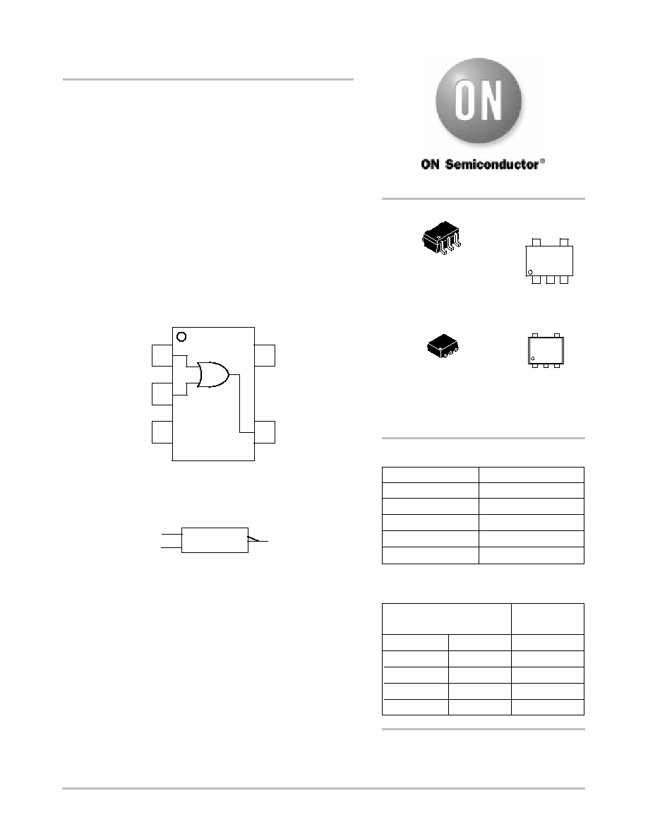
NL17SZ32
Single 2-Input OR Gate
The NL17SZ32 is a single 2-input OR Gate in two tiny footprint
packages. The device performs much as LCX multi-gate products in
speed and drive. They should be used wherever the need for higher
speed and drive are needed.
∑
Tiny SOT- 353 and SOT- 553 Packages
∑
2.4 ns T
PD
at 5 V (typ)
∑
Source/Sink 24 mA at 3.0 V
∑
Over-Voltage Tolerant Inputs
∑
Pin For Pin with NC7SZ32P5X, TC7SZ32FU and TC7SZ32AFE
∑
Chip Complexity: FETs = 20
∑
Designed for 1.65 V to 5.5 V V
CC
Operation
Figure 1. Pinout (Top View)
Figure 2. Logic Symbol
w
1
Y
A
B
V
CC
B
A
1
2
3
5
4
GND
Y
MARKING
DIAGRAMS
L4
d
SOT-353/SC70-5/SC-88A
DF SUFFIX
CASE 419A
SOT-553
XV5 SUFFIX
CASE 463B
L4
= Device Marking
D
= One Digit Date Code
L4 D
1
5
1
5
1
5
1
5
See detailed ordering and shipping information in the package
dimensions section on page 4 of this data sheet.
ORDERING INFORMATION
http://onsemi.com
MARKING
DIAGRAMS
d = Date Code
Input
FUNCTION TABLE
B
L
H
L
H
Output
Y = A
)
B
Y
L
H
H
H
A
L
L
H
H
PIN ASSIGNMENT
Pin
1
2
3
4
5
Function
A
B
GND
Y
V
CC

NL17SZ32
http://onsemi.com
2
MAXIMUM RATINGS
Symbol
Parameter
Value
Unit
V
CC
DC Supply Voltage
*
0.5 to
)
7.0
V
V
IN
DC Input Voltage
*
0.5 to
)
7.0
V
V
OUT
DC Output Voltage
*
0.5 to V
CC
)
0.5
V
I
IK
DC Input Diode Current
*
50
mA
I
OK
DC Output Diode Current
*
50
mA
I
OUT
DC Output Sink Current
$
50
mA
I
CC
DC Supply Current per Supply Pin
$
100
mA
T
STG
Storage Temperature Range
*
65 to
)
150
∞
C
T
L
Lead Temperature, 1 mm from Case for 10 Seconds
260
∞
C
T
J
Junction Temperature Under Bias
)
150
∞
C
q
JA
Thermal Resistance
SOT- 353 (Note 1)
SOT- 553
350
496
∞
C/W
P
D
Power Dissipation in Still Air at 85
∞
C
SOT- 353
SOT- 553
186
135
mW
MSL
Moisture Sensitivity
Level 1
F
R
Flammability Rating
Oxygen Index: 28 to 34
UL 94 V-0 @ 0.125 in
ESD
ESD Classification
Human Body Model (Note 2)
Machine Model (Note 3)
Charged Device Model (Note 4)
Class Z
Class A
N/A
V
Maximum Ratings are those values beyond which damage to the device may occur. Exposure to these conditions or conditions beyond those
indicated may adversely affect device reliability. Functional operation under absolute maximum-rated conditions is not implied. Functional
operation should be restricted to the Recommended Operating Conditions.
1. Measured with minimum pad spacing on an FR4 board, using 10 mm-by-1 inch, 2-ounce copper trace with no air flow.
2. Tested to EIA/JESD22-A114-A, rated to EIA/JESD22-A114-B.
3. Tested to EIA/JESD22-A115-A, rated to EIA/JESD22-A115-A.
4. Tested to JESD22-C101-A.
RECOMMENDED OPERATING CONDITIONS
Symbol
Parameter
Min
Max
Unit
V
CC
DC Supply Voltage
1.65
5.5
V
V
IN
DC Input Voltage
0
5.5
V
V
OUT
DC Output Voltage
0
V
CC
+ 0.5
V
T
A
Operating Temperature Range
*
40
)
85
∞
C
t
r
, t
f
Input Rise and Fall Time
V
CC
= 3.0 V
$
0.3 V
V
CC
= 5.0 V
$
0.5 V
0
0
100
20
ns/V
NL17SZ32
http://onsemi.com
3
DC ELECTRICAL CHARACTERISTICS
V
CC
T
A
= 25
5
C
*
40
5
C
v
T
A
v
85
5
C
Symbol
Parameter
Condition
V
CC
(V)
Min
Typ
Max
Min
Max
Unit
V
IH
High-Level Input Voltage
1.65 to 1.95
2.3 to 5.5
0.75 V
CC
0.7 V
CC
0.75 V
CC
0.7 V
CC
V
V
IL
Low-Level Input Voltage
1.65 to 1.95
2.3 to 5.5
0.25 V
CC
0.3 V
CC
0.25 V
CC
0.3 V
CC
V
V
OH
High- Level Output Voltage
V
IN
= V
IL
or V
IH
I
OH
= 100
m
A
I
OH
= -3 mA
I
OH
= -8 mA
I
OH
= -12 mA
I
OH
= -16 mA
I
OH
= -24 mA
I
OH
= -32 mA
1.65 to 5.5
1.65
2.3
2.7
3.0
3.0
4.5
V
CC
- 0.1
1.29
1.9
2.2
2.4
2.3
3.8
V
CC
1.52
2.1
2.4
2.7
2.5
4.0
V
CC
- 0.1
1.29
1.9
2.2
2.4
2.3
3.8
V
V
OL
Low- Level Output Voltage
V
IN
= V
IH
or V
OH
I
OL
= 100
m
A
I
OL
= 3 mA
I
OL
= 8 mA
I
OL
= 12 mA
I
OL
= 16 mA
I
OL
= 24 mA
I
OL
= 32 mA
1.65 to 5.5
1.65
2.3
2.7
3.0
3.0
4.5
0.08
0.20
0.22
0.28
0.38
0.42
0.1
0.24
0.3
0.4
0.4
0.55
0.55
0.1
0.24
0.3
0.4
0.4
0.55
0.55
V
I
IN
Input Leakage Current
V
IN
= V
CC
or GND
0 to 5.5
$
0.1
$
1.0
m
A
I
CC
Quiescent Supply Current
V
IN
= V
CC
or GND
5.5
1
10
m
A
AC ELECTRICAL CHARACTERISTICS
t
R
= t
F
= 3.0 ns
V
CC
T
A
= 25
5
C
*
40
5
C
v
T
A
v
85
5
C
Symbol
Parameter
Condition
V
CC
(V)
Min
Typ
Max
Min
Max
Unit
t
PLH
Propagation Delay
(Fi
d )
R
L
= 1 M
W,
C
L
= 15 pF
1.65
2.0
5.5
12.0
2.0
12.7
ns
t
PHL
(Figure 3 and 4)
R
L
= 1 M
W,
C
L
= 15 pF
1.8
2.0
4.6
10
2.0
10.5
R
L
= 1 M
W,
C
L
= 15 pF
2.5
$
0.2
0.8
3.0
7
0.8
7.5
R
L
= 1 M
W,
C
L
= 15 pF
3.3
$
0.3
0.5
2.6
4.7
0.5
5.0
R
L
= 500
W,
C
L
= 50 pF
1.5
3.0
5.2
1.5
5.5
R
L
= 1 M
W,
C
L
= 15 pF
5.0
$
0.5
0.5
2.2
4.1
0.5
4.4
R
L
= 500
W,
C
L
= 50 pF
0.8
2.4
4.5
0.8
4.8
CAPACITIVE CHARACTERISTICS
Symbol
Parameter
Condition
Typical
Unit
C
IN
Input Capacitance
V
CC
= 5.5 V, V
I
= 0 V or V
CC
u
4
pF
C
PD
Power Dissipation Capacitance
(
)
10 MHz, V
CC
= 3.3 V, V
I
= 0 V or V
CC
25
pF
(Note 5)
10 MHz, V
CC
= 5.5 V, V
I
= 0 V or V
CC
30
5. C
PD
is defined as the value of the internal equivalent capacitance which is calculated from the operating current consumption without load.
Average operating current can be obtained by the equation: I
CC(OPR
)
= C
PD
V
CC
f
in
+ I
CC
. C
PD
is used to determine the no-load dynamic
power consumption; P
D
= C
PD
V
CC
2
f
in
+ I
CC
V
CC
.
NL17SZ32
http://onsemi.com
4
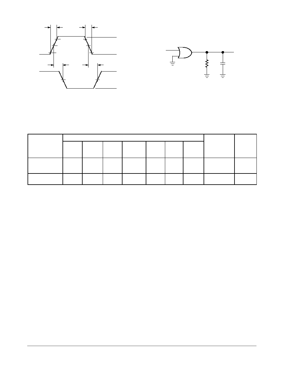
Figure 3. Switching Waveform
R
L
C
L
A 1 MHz square input wave is recommended for
propagation delay tests.
Figure 4. Test Circuit
t
f
= 3 ns
V
CC
GND
V
OH
V
OL
90%
50%
10%
50%
t
PLH
t
PHL
OUTPUT Y
INPUT
A and B
t
f
= 3 ns
90%
50%
10%
50%
OUTPUT
INPUT
DEVICE ORDERING INFORMATION
Device Nomenclature
Device Order
Number
Logic
Circuit
Indicator
No. of
Gates per
Package
Temp
Range
Identifier
Technology
Device
Function
Package
Suffix
Tape and
Reel
Suffix
Package
Type
Tape and
Reel Size
NL17SZ32DFT2
NL
1
7
SZ
32
DF
T2
SC70-5/
SC-88A/
SOT-353
178 mm,
3000 Units
NL17SZ32XV5T2
NL
1
7
SZ
32
XV5
T2
SOT-553
178 mm
4000 units

NL17SZ32
http://onsemi.com
5
TAPE TRAILER
(Connected to Reel Hub)
NO COMPONENTS
160 mm MIN
TAPE LEADER
NO COMPONENTS
400 mm MIN
COMPONENTS
DIRECTION OF FEED
CAVITY
TAPE
TOP TAPE
Figure 5. Tape Ends for Finished Goods
"T2" Pin One Opposing Sprocket Hole (3k Reel)
Figure 6. SOT-353/SC70-5/SC-88A Reel Configuration/Orientation
"T2" Pin One Opposing Sprocket Hole (4k Reel)
Figure 7. SOT-553 XV5T2 Reel Configuration/Orientation