©
Semiconductor Components Industries, LLC, 2002
June, 2002 ≠ Rev. 0
1
Publication Order Number:
NLAS4053/D
NLAS4053
Analog Multiplexer/
Demultiplexer
Triple 2:1 Analog Switch≠Multiplexer
Improved Process, Sub≠Micron Silicon
Gate CMOS
The NLAS4053 is an improved version of the MC14053 and
MC74HC4053 fabricated in sub≠micron Silicon Gate CMOS
technology for lower R
DS(on)
resistance and improved linearity with
low current. This device may be operated either with a single supply or
dual supply up to
±
3 V to pass a 6 V
PP
signal without coupling
capacitors.
When operating in single supply mode, it is only necessary to tie
V
EE
, pin 7 to ground. For dual supply operation, V
EE
is tied to a
negative voltage, not to exceed maximum ratings. Pin for pin
compatible with all industry standard versions of `4053.'
∑
Improved R
DS(on)
Specifications
∑
Pin for Pin Replacement for MAX4053 and MAX4053A
≠ One Half the Resistance Operating at 5.0 Volts
∑
Single or Dual Supply Operation
≠ Single 3≠5 Volt Operation, or Dual
±
3 Volt Operation
≠ With V
CC
of 3.0 to 3.3 V, Device Can Interface with 1.8 V Logic,
≠
No Translators Needed
≠ Address and Inhibit Pins are Over≠Voltage Tolerant and May Be
≠
Driven Up +6 V Regardless of V
CC
∑
Address and Control Pins are Standard TTL Compatible
≠ Greatly Improved Noise Margin Over MAX4053 and MAX4053A
∑
Improved Linearity Over Standard HC4053 Devices
∑
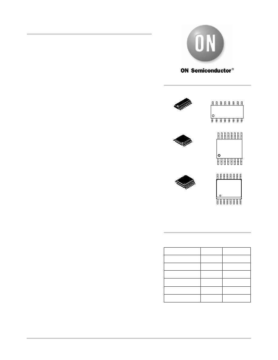
Popular SOIC, and Space Saving TSSOP, and QSOP 16 Pin
Packages
SO≠16
D SUFFIX
CASE 751B
TSSOP≠16
DT SUFFIX
CASE 948F
1
8
9
16
NLAS4053
AWLYWW
MARKING DIAGRAMS
NLAS
4053
ALYW
A
= Assembly Location
L, WL
= Wafer Lot
Y, YY
= Year
W, WW
= Work Week
ORDERING INFORMATION
Device
Package
Shipping
NLAS4053D
SO≠16
48 Units/Rail
NLAS4053DR2
SO≠16
2500 Units/Reel
NLAS4053DT
TSSOP≠16
96 Units/Rail
NLAS4053DTR2
TSSOP≠16
2500 Units/Reel
NLAS4053QS
QSOP≠16
48 Units/Rail
NLAS4053QSR
QSOP≠16
2000 Units/Reel
QSOP≠16
QS SUFFIX
CASE 492
NLAS
4053
ALYW
1
8
16
9
1
8
16
9
http://onsemi.com
NLAS4053
http://onsemi.com
2
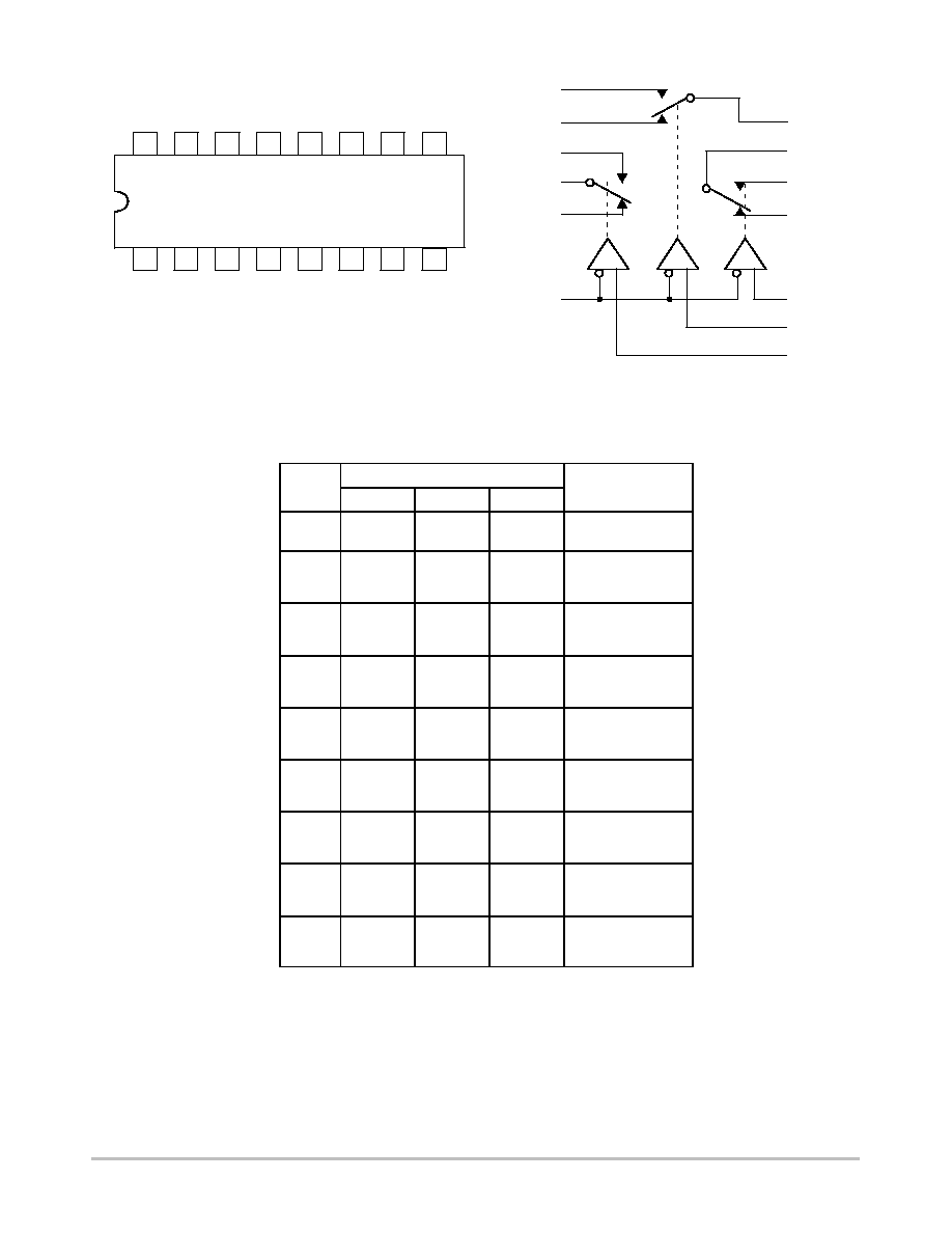
Figure 1. Pin Connection
(Top View)
Figure 2. Logic Diagram
15
16
14
13
12
11
10
2
1
3
4
5
6
7
V
CC
9
8
COM
B
COM
C
NO
C
NC
C
Add
C
Add
B
Add
A
NO
B
NC
B
NO
A
COM
A
NC
A
Inhibit
V
EE
GND
COM
B
COM
C
NO
C
NC
C
C
B
A
NO
B
NC
B
NO
A
COM
A
NC
A
Enable
TRUTH TABLE
Address
Inhibit
C
B
A
ON SWITCHES*
1
X
don't care
X
don't care
X
don't care
All switches open
0
0
0
0
COM
A
≠NC
A
,
COM
B
≠NC
B
,
COM
C
≠NC
C
0
0
0
1
COM
A
≠NO
A
,
COM
B
≠NC
B
,
COM
C
≠NC
C
0
0
1
0
COM
A
≠NC
A
,
COM
B
≠NO
B
,
COM
C
≠NC
C
0
0
1
1
COM
A
≠NO
A
,
COM
B
≠NO
B
,
COM
C
≠NC
C
0
1
0
0
COM
A
≠NC
A
,
COM
B
≠NC
B
,
COM
C
≠NO
C
0
1
0
1
COM
A
≠NO
A
,
COM
B
≠NC
B
,
COM
C
≠NO
C
0
1
1
0
COM
A
≠NC
A
,
COM
B
≠NO
B
,
COM
C
≠NO
C
0
1
1
1
COM
A
≠NO
A
,
COM
B
≠NO
B
,
COM
C
≠NO
C
*NO, NC, and COM pins are identical and interchangeable. Either may be
considered an input or output; signals pass equally well in either direction.

NLAS4053
http://onsemi.com
3
ŒŒŒŒŒŒŒŒŒŒŒŒŒŒŒŒŒŒŒŒŒŒŒŒŒŒŒŒŒŒŒŒŒ
ŒŒŒŒŒŒŒŒŒŒŒŒŒŒŒŒŒŒŒŒŒŒŒŒŒŒŒŒŒŒŒŒŒ
MAXIMUM RATINGS
(Note 1)
ŒŒŒŒŒ
ŒŒŒŒŒ
Symbol
ŒŒŒŒŒŒŒŒŒŒŒŒŒŒŒŒŒŒŒŒŒ
ŒŒŒŒŒŒŒŒŒŒŒŒŒŒŒŒŒŒŒŒŒ
Parameter
ŒŒŒŒŒŒŒ
ŒŒŒŒŒŒŒ
Value
ŒŒŒ
ŒŒŒ
Unit
ŒŒŒŒŒ
ŒŒŒŒŒ
V
EE
ŒŒŒŒŒŒŒŒŒŒŒŒŒŒŒŒŒŒŒŒŒ
ŒŒŒŒŒŒŒŒŒŒŒŒŒŒŒŒŒŒŒŒŒ
Negative DC Supply Voltage
(Referenced to GND)
ŒŒŒŒŒŒŒ
ŒŒŒŒŒŒŒ
≠7.0 to
)
0.5
ŒŒŒ
ŒŒŒ
V
ŒŒŒŒŒ
ŒŒŒŒŒ
V
CC
ŒŒŒŒŒŒŒŒŒŒŒŒŒŒŒŒŒŒŒŒŒ
ŒŒŒŒŒŒŒŒŒŒŒŒŒŒŒŒŒŒŒŒŒ
Positive DC Supply Voltage (Note 2)
(Referenced to GND)
(Referenced to V
EE
)
ŒŒŒŒŒŒŒ
ŒŒŒŒŒŒŒ
≠0.5 to
)
7.0
≠0.5 to
)
7.0
ŒŒŒ
ŒŒŒ
V
ŒŒŒŒŒ
ŒŒŒŒŒ
V
IS
ŒŒŒŒŒŒŒŒŒŒŒŒŒŒŒŒŒŒŒŒŒ
ŒŒŒŒŒŒŒŒŒŒŒŒŒŒŒŒŒŒŒŒŒ
Analog Input Voltage
ŒŒŒŒŒŒŒ
ŒŒŒŒŒŒŒ
V
EE
≠0.5 to V
CC
)
0.5
ŒŒŒ
ŒŒŒ
V
ŒŒŒŒŒ
ŒŒŒŒŒ
V
IN
ŒŒŒŒŒŒŒŒŒŒŒŒŒŒŒŒŒŒŒŒŒ
ŒŒŒŒŒŒŒŒŒŒŒŒŒŒŒŒŒŒŒŒŒ
Digital Input Voltage
(Referenced to GND)
ŒŒŒŒŒŒŒ
ŒŒŒŒŒŒŒ
≠0.5 to 7.0
ŒŒŒ
ŒŒŒ
V
ŒŒŒŒŒ
ŒŒŒŒŒ
I
ŒŒŒŒŒŒŒŒŒŒŒŒŒŒŒŒŒŒŒŒŒ
ŒŒŒŒŒŒŒŒŒŒŒŒŒŒŒŒŒŒŒŒŒ
DC Current, Into or Out of Any Pin
ŒŒŒŒŒŒŒ
ŒŒŒŒŒŒŒ
$
50
ŒŒŒ
ŒŒŒ
mA
ŒŒŒŒŒ
ŒŒŒŒŒ
T
STG
ŒŒŒŒŒŒŒŒŒŒŒŒŒŒŒŒŒŒŒŒŒ
ŒŒŒŒŒŒŒŒŒŒŒŒŒŒŒŒŒŒŒŒŒ
Storage Temperature Range
ŒŒŒŒŒŒŒ
ŒŒŒŒŒŒŒ
≠65 to
)
150
ŒŒŒ
ŒŒŒ
_
C
ŒŒŒŒŒ
ŒŒŒŒŒ
T
L
ŒŒŒŒŒŒŒŒŒŒŒŒŒŒŒŒŒŒŒŒŒ
ŒŒŒŒŒŒŒŒŒŒŒŒŒŒŒŒŒŒŒŒŒ
Lead Temperature, 1 mm from Case for 10 Seconds
ŒŒŒŒŒŒŒ
ŒŒŒŒŒŒŒ
260
ŒŒŒ
ŒŒŒ
_
C
ŒŒŒŒŒ
ŒŒŒŒŒ
T
J
ŒŒŒŒŒŒŒŒŒŒŒŒŒŒŒŒŒŒŒŒŒ
ŒŒŒŒŒŒŒŒŒŒŒŒŒŒŒŒŒŒŒŒŒ
Junction Temperature under Bias
ŒŒŒŒŒŒŒ
ŒŒŒŒŒŒŒ
)
150
ŒŒŒ
ŒŒŒ
_
C
ŒŒŒŒŒ
Œ
ŒŒŒ
Œ
ŒŒŒŒŒ
q
JA
ŒŒŒŒŒŒŒŒŒŒŒŒŒŒŒŒŒŒŒŒŒ
Œ
ŒŒŒŒŒŒŒŒŒŒŒŒŒŒŒŒŒŒŒ
Œ
ŒŒŒŒŒŒŒŒŒŒŒŒŒŒŒŒŒŒŒŒŒ
Thermal Resistance
SOIC
TSSOP
QSOP
ŒŒŒŒŒŒŒ
Œ
ŒŒŒŒŒ
Œ
ŒŒŒŒŒŒŒ
143
164
164
ŒŒŒ
Œ
Œ
Œ
ŒŒŒ
∞
C/W
ŒŒŒŒŒ
Œ
ŒŒŒ
Œ
ŒŒŒŒŒ
P
D
ŒŒŒŒŒŒŒŒŒŒŒŒŒŒŒŒŒŒŒŒŒ
Œ
ŒŒŒŒŒŒŒŒŒŒŒŒŒŒŒŒŒŒŒ
Œ
ŒŒŒŒŒŒŒŒŒŒŒŒŒŒŒŒŒŒŒŒŒ
Power Dissipation in Still Air,
SOIC
TSSOP
QSOP
ŒŒŒŒŒŒŒ
Œ
ŒŒŒŒŒ
Œ
ŒŒŒŒŒŒŒ
500
450
450
ŒŒŒ
Œ
Œ
Œ
ŒŒŒ
mW
ŒŒŒŒŒ
ŒŒŒŒŒ
MSL
ŒŒŒŒŒŒŒŒŒŒŒŒŒŒŒŒŒŒŒŒŒ
ŒŒŒŒŒŒŒŒŒŒŒŒŒŒŒŒŒŒŒŒŒ
Moisture Sensitivity
ŒŒŒŒŒŒŒ
ŒŒŒŒŒŒŒ
Level 1
ŒŒŒ
ŒŒŒ
ŒŒŒŒŒ
ŒŒŒŒŒ
F
R
ŒŒŒŒŒŒŒŒŒŒŒŒŒŒŒŒŒŒŒŒŒ
ŒŒŒŒŒŒŒŒŒŒŒŒŒŒŒŒŒŒŒŒŒ
Flammability Rating
Oxygen Index: 30% ≠ 35%
ŒŒŒŒŒŒŒ
ŒŒŒŒŒŒŒ
UL 94 V≠0 @ 0.125 in
ŒŒŒ
ŒŒŒ
ŒŒŒŒŒ
Œ
ŒŒŒ
Œ
Œ
ŒŒŒ
Œ
ŒŒŒŒŒ
V
ESD
ŒŒŒŒŒŒŒŒŒŒŒŒŒŒŒŒŒŒŒŒŒ
Œ
ŒŒŒŒŒŒŒŒŒŒŒŒŒŒŒŒŒŒŒ
Œ
Œ
ŒŒŒŒŒŒŒŒŒŒŒŒŒŒŒŒŒŒŒ
Œ
ŒŒŒŒŒŒŒŒŒŒŒŒŒŒŒŒŒŒŒŒŒ
ESD Withstand Voltage
Human Body Model (Note 3)
Machine Model (Note 4)
Charged Device Model (Note 5)
ŒŒŒŒŒŒŒ
Œ
ŒŒŒŒŒ
Œ
Œ
ŒŒŒŒŒ
Œ
ŒŒŒŒŒŒŒ
u
2000
u
200
u
1000
ŒŒŒ
Œ
Œ
Œ
Œ
Œ
Œ
ŒŒŒ
V
ŒŒŒŒŒ
ŒŒŒŒŒ
I
LATCH≠UP
ŒŒŒŒŒŒŒŒŒŒŒŒŒŒŒŒŒŒŒŒŒ
ŒŒŒŒŒŒŒŒŒŒŒŒŒŒŒŒŒŒŒŒŒ
Latch≠Up Performance
Above V
CC
and Below GND at 125
∞
C (Note 6)
ŒŒŒŒŒŒŒ
ŒŒŒŒŒŒŒ
$
300
ŒŒŒ
ŒŒŒ
mA
1. Absolute maximum continuous ratings are those values beyond which damage to the device may occur. Extended exposure to these
conditions or conditions beyond those indicated may adversely affect device reliability. Functional operation under absolute maximum≠rated
conditions is not implied.
2. The absolute value of V
CC
$
|V
EE
|
7.0.
3. Tested to EIA/JESD22≠A114≠A.
4. Tested to EIA/JESD22≠A115≠A.
5. Tested to JESD22≠C101≠A.
6. Tested to EIA/JESD78.
RECOMMENDED OPERATING CONDITIONS
Symbol
Parameter
Min
Max
Unit
ŒŒŒŒ
ŒŒŒŒ
V
EE
ŒŒŒŒŒŒŒŒŒŒŒŒŒŒŒŒŒŒŒŒŒŒ
ŒŒŒŒŒŒŒŒŒŒŒŒŒŒŒŒŒŒŒŒŒŒ
Negative DC Supply Voltage
(Referenced to GND)
ŒŒŒŒ
ŒŒŒŒ
≠5.5
ŒŒŒŒ
ŒŒŒŒ
GND
ŒŒŒ
ŒŒŒ
V
ŒŒŒŒ
Œ
ŒŒ
Œ
ŒŒŒŒ
V
CC
ŒŒŒŒŒŒŒŒŒŒŒŒŒŒŒŒŒŒŒŒŒŒ
Œ
ŒŒŒŒŒŒŒŒŒŒŒŒŒŒŒŒŒŒŒŒ
Œ
ŒŒŒŒŒŒŒŒŒŒŒŒŒŒŒŒŒŒŒŒŒŒ
Positive DC Supply Voltage
(Referenced to GND)
(Referenced to V
EE
)
ŒŒŒŒ
Œ
ŒŒ
Œ
ŒŒŒŒ
2.5
2.5
ŒŒŒŒ
Œ
ŒŒ
Œ
ŒŒŒŒ
5.5
6.6
ŒŒŒ
Œ
Œ
Œ
ŒŒŒ
V
ŒŒŒŒ
ŒŒŒŒ
V
IS
ŒŒŒŒŒŒŒŒŒŒŒŒŒŒŒŒŒŒŒŒŒŒ
ŒŒŒŒŒŒŒŒŒŒŒŒŒŒŒŒŒŒŒŒŒŒ
Analog Input Voltage
ŒŒŒŒ
ŒŒŒŒ
V
EE
ŒŒŒŒ
ŒŒŒŒ
V
CC
ŒŒŒ
ŒŒŒ
V
ŒŒŒŒ
ŒŒŒŒ
V
IN
ŒŒŒŒŒŒŒŒŒŒŒŒŒŒŒŒŒŒŒŒŒŒ
ŒŒŒŒŒŒŒŒŒŒŒŒŒŒŒŒŒŒŒŒŒŒ
Digital Input Voltage
(Note 7) (Referenced to GND)
ŒŒŒŒ
ŒŒŒŒ
0
ŒŒŒŒ
ŒŒŒŒ
5.5
ŒŒŒ
ŒŒŒ
V
ŒŒŒŒ
ŒŒŒŒ
T
A
ŒŒŒŒŒŒŒŒŒŒŒŒŒŒŒŒŒŒŒŒŒŒ
ŒŒŒŒŒŒŒŒŒŒŒŒŒŒŒŒŒŒŒŒŒŒ
Operating Temperature Range, All Package Types
ŒŒŒŒ
ŒŒŒŒ
≠55
ŒŒŒŒ
ŒŒŒŒ
125
ŒŒŒ
ŒŒŒ
_
C
ŒŒŒŒ
ŒŒŒŒ
t
r
, t
f
ŒŒŒŒŒŒŒŒŒŒŒŒŒŒŒŒŒŒŒŒŒŒ
ŒŒŒŒŒŒŒŒŒŒŒŒŒŒŒŒŒŒŒŒŒŒ
Input Rise/Fall Time
V
CC
= 3.0 V
$
0.3 V
(Channel Select or Enable Inputs)
V
CC
= 5.0 V
$
0.5 V
ŒŒŒŒ
ŒŒŒŒ
0
0
ŒŒŒŒ
ŒŒŒŒ
100
20
ŒŒŒ
ŒŒŒ
ns/V
7. Unused digital inputs may not be left open. All digital inputs must be tied to a high≠logic voltage level or a low≠logic input voltage level.
NLAS4053
http://onsemi.com
4
DC CHARACTERISTICS ≠ Digital Section
(Voltages Referenced to GND)
V
CC
Guaranteed Limit
Symbol
Parameter
Condition
V
CC
V
≠55 to 25
∞
C
v
85
∞
C
v
125
∞
C
Unit
V
IH
Minimum High≠Level Input Voltage,
Address and Inhibit Inputs
2.0
3.0
4.5
5.5
1.5
2.1
3.15
3.85
1.5
2.1
3.15
3.85
1.5
2.1
3.15
3.85
V
V
IL
Maximum Low≠Level Input Voltage,
Address and Inhibit Inputs
2.0
3.0
4.5
5.5
0.5
0.9
1.35
1.65
0.5
0.9
1.35
1.65
0.5
0.9
1.35
1.65
V
I
IN
Maximum Input Leakage Current,
Address or Inhibit Inputs
V
IN
= 6.0 or GND
0 V to 6.0 V
$
0.1
$
1.0
$
1.0
m
A
I
CC
Maximum Quiescent Supply
Current (per Package)
Channel Select, Enable and
V
IS
= V
CC
or GND
6.0
4.0
40
80
m
A
DC ELECTRICAL CHARACTERISTICS ≠ Analog Section
ŒŒŒŒ
ŒŒŒŒ
ŒŒŒŒŒŒŒŒ
ŒŒŒŒŒŒŒŒ
ŒŒŒŒŒŒŒŒŒŒ
ŒŒŒŒŒŒŒŒŒŒ
ŒŒ
ŒŒ
V
CC
ŒŒŒ
ŒŒŒ
V
EE
ŒŒŒŒŒŒŒŒŒŒ
ŒŒŒŒŒŒŒŒŒŒ
Guaranteed Limit
ŒŒ
ŒŒ
ŒŒŒŒ
ŒŒŒŒ
Symbol
ŒŒŒŒŒŒŒŒ
ŒŒŒŒŒŒŒŒ
Parameter
ŒŒŒŒŒŒŒŒŒŒ
ŒŒŒŒŒŒŒŒŒŒ
Test Conditions
ŒŒ
ŒŒ
V
CC
V
ŒŒŒ
ŒŒŒ
V
EE
V
ŒŒŒŒŒ
ŒŒŒŒŒ
≠55 to 25
∞
C
ŒŒŒ
ŒŒŒ
v
85
_
C
ŒŒŒŒ
ŒŒŒŒ
v
125
_
C
ŒŒ
ŒŒ
Unit
ŒŒŒŒ
Œ
ŒŒ
Œ
Œ
ŒŒ
Œ
ŒŒŒŒ
R
ON
ŒŒŒŒŒŒŒŒ
Œ
ŒŒŒŒŒŒ
Œ
Œ
ŒŒŒŒŒŒ
Œ
ŒŒŒŒŒŒŒŒ
Maximum "ON" Resistance
ŒŒŒŒŒŒŒŒŒŒ
Œ
ŒŒŒŒŒŒŒŒ
Œ
Œ
ŒŒŒŒŒŒŒŒ
Œ
ŒŒŒŒŒŒŒŒŒŒ
V
IN
= V
IL
or V
IH
V
IS
= V
EE
to V
CC
|I
S
| = 10 mA
(Figures 4 thru 9)
ŒŒ
ŒŒ
ŒŒ
ŒŒ
3.0
4.5
3.0
ŒŒŒ
Œ
Œ
Œ
Œ
Œ
Œ
ŒŒŒ
0
0
≠3.0
ŒŒŒŒŒ
Œ
ŒŒŒ
Œ
Œ
ŒŒŒ
Œ
ŒŒŒŒŒ
86
37
26
ŒŒŒ
Œ
Œ
Œ
Œ
Œ
Œ
ŒŒŒ
108
46
33
ŒŒŒŒ
Œ
ŒŒ
Œ
Œ
ŒŒ
Œ
ŒŒŒŒ
120
55
37
ŒŒ
ŒŒ
ŒŒ
ŒŒ
W
ŒŒŒŒ
Œ
ŒŒ
Œ
Œ
ŒŒ
Œ
ŒŒŒŒ
R
ON
ŒŒŒŒŒŒŒŒ
Œ
ŒŒŒŒŒŒ
Œ
Œ
ŒŒŒŒŒŒ
Œ
ŒŒŒŒŒŒŒŒ
Maximum Difference in "ON"
Resistance Between Any
Two Channels in the Same
Package
ŒŒŒŒŒŒŒŒŒŒ
Œ
ŒŒŒŒŒŒŒŒ
Œ
Œ
ŒŒŒŒŒŒŒŒ
Œ
ŒŒŒŒŒŒŒŒŒŒ
V
IN
= V
IL
or V
IH,
V
IS
= 2.0 V
V
IS
= 3.5 V
|I
S
| = 10 mA,
V
IS
= 2.0 V
ŒŒ
ŒŒ
ŒŒ
ŒŒ
3.0
4.5
3.0
ŒŒŒ
Œ
Œ
Œ
Œ
Œ
Œ
ŒŒŒ
0
0
≠3.0
ŒŒŒŒŒ
Œ
ŒŒŒ
Œ
Œ
ŒŒŒ
Œ
ŒŒŒŒŒ
15
13
10
ŒŒŒ
Œ
Œ
Œ
Œ
Œ
Œ
ŒŒŒ
20
18
15
ŒŒŒŒ
Œ
ŒŒ
Œ
Œ
ŒŒ
Œ
ŒŒŒŒ
20
18
15
ŒŒ
ŒŒ
ŒŒ
ŒŒ
W
R
flat(ON)
COM≠NO
On≠Resistance Flatness
V
com
1, 2, 3.5 V
V
com
≠2, 0, 2 V
|I
S
| = 10 mA
4.5
3.0
0
≠3.0
4
2
4
2
5
3
W
I
NC(OFF)
I
NO(OFF)
Maximum Off≠Channel
Leakage Current
Switch Off
V
IN
= V
IL
or V
IH
V
IO
= V
CC
≠1.0 V or V
EE
+1.0 V
(Figure 17)
6.0
3.0
0
≠3.0
0.1
0.1
5.0
5.0
100
100
nA
I
COM(ON)
Maximum On≠Channel
Leakage Current,
Channel≠ to≠Channel
Switch On
V
IO
= V
CC
≠1.0 V or V
EE
+1.0 V
(Figure 17)
6.0
3.0
0
≠3.0
0.1
0.1
5.0
5.0
100
100
nA
NLAS4053
http://onsemi.com
5
AC CHARACTERISTICS
(Input t
r
= t
f
= 3 ns)
ŒŒŒŒ
ŒŒŒŒ
ŒŒŒŒŒŒŒŒŒ
ŒŒŒŒŒŒŒŒŒ
ŒŒŒŒŒŒŒŒ
ŒŒŒŒŒŒŒŒ
ŒŒ
ŒŒ
ŒŒŒ
ŒŒŒ
ŒŒŒŒŒŒŒŒŒŒŒ
ŒŒŒŒŒŒŒŒŒŒŒ
Guaranteed Limit
ŒŒ
ŒŒ
ŒŒŒŒ
ŒŒŒŒ
ŒŒŒŒŒŒŒŒŒ
ŒŒŒŒŒŒŒŒŒ
ŒŒŒŒŒŒŒŒ
ŒŒŒŒŒŒŒŒ
ŒŒ
ŒŒ
V
CC
ŒŒŒ
ŒŒŒ
V
EE
ŒŒŒŒŒŒ
ŒŒŒŒŒŒ
≠55 to 25
_
C
ŒŒŒ
ŒŒŒ
ŒŒŒŒ
ŒŒŒŒ
ŒŒ
ŒŒ
ŒŒŒŒ
ŒŒŒŒ
Symbol
ŒŒŒŒŒŒŒŒŒ
ŒŒŒŒŒŒŒŒŒ
Parameter
ŒŒŒŒŒŒŒŒ
ŒŒŒŒŒŒŒŒ
Test Conditions
ŒŒ
ŒŒ
V
CC
V
ŒŒŒ
ŒŒŒ
V
EE
V
ŒŒŒ
ŒŒŒ
Min
ŒŒŒŒ
ŒŒŒŒ
Typ*
ŒŒŒ
ŒŒŒ
v
85
_
C
ŒŒŒŒ
ŒŒŒŒ
v
125
_
C
ŒŒ
ŒŒ
Unit
t
BBM
Minimum Break≠Before≠Make
Time
V
IN
= V
IL
or V
IH
V
IS
= V
CC
R
L
= 300
W,
C
L
= 35 pF
(Figure 19)
3.0
4.5
3.0
0.0
0.0
≠3.0
1.0
1.0
1.0
6.5
5.0
3.5
≠
≠
≠
≠
≠
≠
ns
*Typical Characteristics are at 25
_
C.
AC CHARACTERISTICS
(C
L
= 50 pF, Input t
r
= t
f
= 3 ns)
Guaranteed Limit
V
CC
V
EE
≠55 to 25
∞
C
v
85
∞
C
v
125
∞
C
Symbol
Parameter
V
CC
V
V
EE
V
Min
Typ
Max
Min
Max
Min
Max
Unit
t
TRANS
Transition Time
(Address Selection Time)
(Figure 18)
2.5
3.0
4.5
3.0
0
0
0
≠3.0
40
28
23
23
45
30
25
25
50
35
30
28
ns
t
ON
Turn≠on Time
(Figures 14, 15, 20, and 21)
Enable to N
O
or N
C
2.5
3.0
4.5
3.0
0
0
0
≠3.0
40
28
23
23
45
30
25
25
50
35
30
28
ns
t
OFF
Turn≠off Time
(Figures 14, 15, 20, and 21)
Enable to N
O
or N
C
2.5
3.0
4.5
3.0
0
0
0
≠3.0
40
28
23
23
45
30
25
25
50
35
30
28
ns
Typical @ 25
∞
C, V
CC
= 5.0 V
C
IN
Maximum Input Capacitance,Select Inputs
8
pF
C
NO
or C
NC
Analog I/O
10
C
COM
Common I/O
10
C
(ON)
Feedthrough
1.0