 | –≠–ª–µ–∫—Ç—Ä–æ–Ω–Ω—ã–π –∫–æ–º–ø–æ–Ω–µ–Ω—Ç: NLAS4783 | –°–∫–∞—á–∞—Ç—å:  PDF PDF  ZIP ZIP |
©
Semiconductor Components Industries, LLC, 2005
March, 2005 - Rev. 0
1
Publication Order Number:
NLAS4783/D
NLAS4783
Triple SPDT 1 Ohm R
ON
Switch
The NLAS4783 is a triple independent ultra-low R
ON
SPDT analog
switch with ENABLE. This device is designed for low operating
voltage, high current switching of speaker output for cell phone
applications. It can switch a balanced stereo output. The NLAS4783
can handle a balanced microphone/speaker/ring-tone generator in a
monophone mode. The device contains a break-make feature.
Features
∑
Single Supply Operation
1.65 to 4.7 V V
CC
Function Directly from LiON Battery
∑
Tiny 3 x 3 mm 16-Pin QFN Package
Meets JEDEC MO-220 Specifications
∑
Low Static Power
∑
OVT on Logic Address and Enable Inputs
∑
This is a Pb-Free Device*
Typical Applications
∑
Cell Phone Speaker/Microphone Switching
∑
Ringtone-Chip/Amplifier Switching
∑
Three Unbalanced (Single-Ended) Switches
∑
Stereo Balanced (Push-Pull) Switching
Important Information
∑
ESD Protection:
Human Body Model (HBM) > 8000 V
Machine Model (MM) > 400 V
∑
Ringtone-Chip/Amplifier Switching
∑
Continuous Current Rating Through each Switch
±
300 mA
∑
Conforms to: JEDEC MO-220, Issue H, Variation VEED-6
∑
Pin-for-Pin Compatible with MAX4783
*For additional information on our Pb-Free strategy and soldering details, please
download the ON Semiconductor Soldering and Mounting Techniques
Reference Manual, SOLDERRM/D.
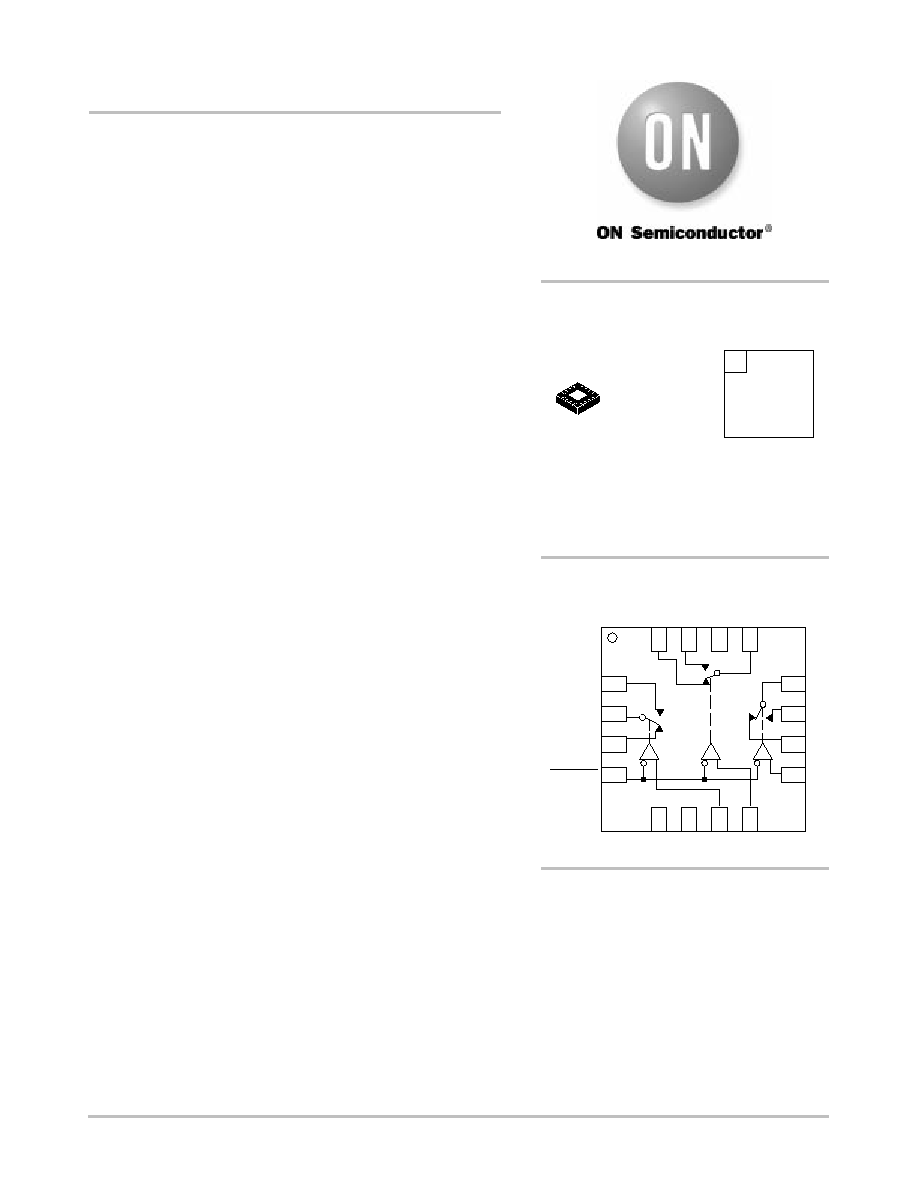
QFN-16
CASE 485AE
1
16
NLAS
4783
ALYW
G
1
A = Assembly Location
L
= Wafer Lot
Y = Year
W = Work Week
G
= Pb-Free Package
««
««
MARKING
DIAGRAM
PIN CONNECTIONS
4
1
16
13
9
12
5
8
14
7
15
6
3
10
2
11
Y0
Y1
Vcc
Y
NC GND
C
B
A
X0
X1
X
Z0
Z
Z1
ENABLE
See detailed ordering and shipping information in the package
dimensions section on page 9 of this data sheet.
ORDERING INFORMATION
http://onsemi.com

NLAS4783
http://onsemi.com
2
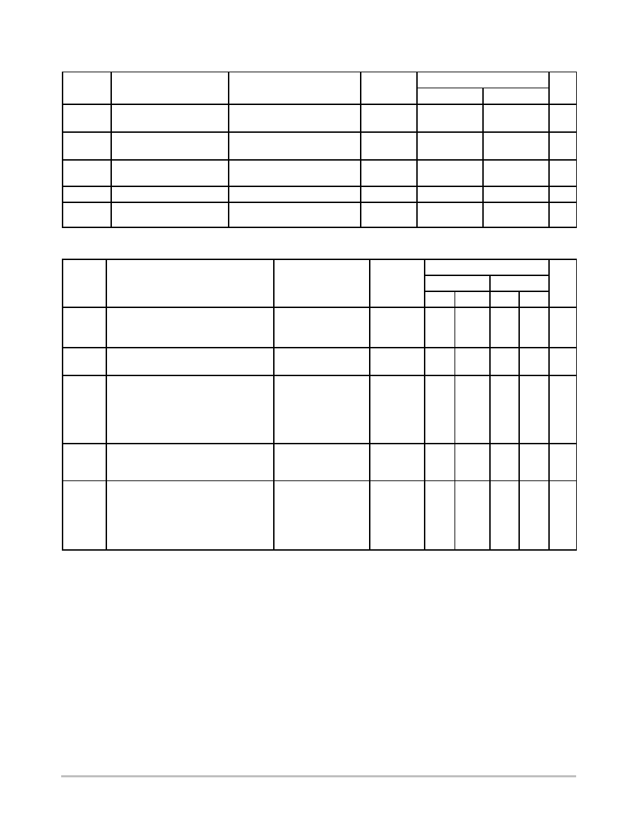
Figure 1. Input Equivalent Circuit
X0, Y0, or Z0
X1, Y1, or Z1
LOGIC
ENABLE
A, B, or C
X, Y, or Z
PIN FUNCTION DESCRIPTION
QFN PIN #
Symbol
Description
15
Y1
Analog Switch Y Normally Open Input
16
Y0
Analog Switch Y Normally Closed Input
1
Z1
Analog Switch Z Normally Open Input
2
Z
Analog Switch Z Output
3
Z0
Analog Switch Z Normally Closed Input
4
ENABLE
Digital Enable Input. Normally connect to GND. Drive to logic high to set all switches off.
5
NC
No Connection. Not internally connected.
6
GND
Ground
7
C
Digital Address C Input
8
B
Digital Address B Input
9
A
Digital Address A Input
10
X0
Analog Switch X Normally Closed Input
11
X1
Analog Switch X Normally Open Input
12
X
Analog Switch X Output
13
Y
Analog Switch Y Output
14
V
CC
Positive Analog and Digital Supply Voltage Input
NLAS4783
http://onsemi.com
3
TRUTH TABLE/SWITCH PROGRAMMING
Select Input
Enable Input
C
B
A
H
X
X
X
All Switches Open
L
L
L
L
X-X0
Y-Y0
Z-Z0
L
L
L
H
X-X1
Y-Y0
Z-Z0
L
L
H
L
X-X0
Y-Y1
Z-Z0
L
L
H
H
X-X1
Y-Y1
Z-Z0
L
H
L
L
X-X0
Y-Y0
Z-Z1
L
H
L
H
X-X1
Y-Y0
Z-Z1
L
H
H
L
X-X0
Y-Y1
Z-Z1
L
H
H
H
X-X1
Y-Y1
Z-Z1
1. Input and output pins are identical and interchangeable. Both pins can be considered input or output. Bidirectional signal pass.
MAXIMUM RATINGS
Symbol
Parameter
Value
Unit
V
CC
Positive DC Supply Voltage
*
0.5 to
)
5.0
V
V
IS
Analog Input Voltage (V
NO
, V
NC
, or V
COM
)
*
0.5 to V
CC
)
0.5
V
V
IN
Digital Select Input Voltage
*
0.5 to
)
5.0
V
I
anl1
Continuous DC Current from COM to NC/NO
$
300
mA
I
anl-pk 1
Peak Current from COM to NC/NO, 10 Duty Cycles (Note 2)
$
500
mA
I
clmp
Continuous DC Current into COM/NC/NO with Respect to V
CC
or GND
$
100
mA
Maximum ratings are those values beyond which device damage can occur. Maximum ratings applied to the device are individual stress limit
values (not normal operating conditions) and are not valid simultaneously. If these limits are exceeded, device functional operation is not implied,
damage may occur and reliability may be affected.
2. Defined as 10% ON, 90% off duty cycle.
RECOMMENDED OPERATING CONDITIONS
Symbol
Parameter
Min
Max
Unit
V
CC
Positive DC Supply Voltage
1.65
4.7
V
V
IS
Analog Input Voltage (V
NO
, V
NC
, or V
COM
)
-
V
CC
V
V
IN
Digital Select Input Voltage
-
V
CC
V
T
A
Operating Temperature Range
*
40
85
∞
C
t
r
, t
f
Input Rise or Fall Time, SELECT
V
CC
= 1.6-2.7 V
V
CC
= 3.0-3.6 V
-
-
20
10
ns/V
NLAS4783
http://onsemi.com
4
DC CHARACTERISTICS - Digital Section (Voltages Referenced to GND)
Guaranteed Limit
Symbol
Parameter
Condition
V
CC
$
10%
*
40
5
C to 25
5
C
t
85
5
C
Unit
V
IH
Minimum High-Level Input
Voltage, Select Inputs
1.65
2.7-4.7
1.0
1.4
1.0
1.4
V
V
IL
Maximum Low-Level Input
Voltage, Select Inputs
1.65
2.7-4.7
0.4
0.5
0.4
0.5
V
I
IN
Maximum Input Leakage
Current, Select Inputs
V
IN
= 5.0 V or GND
4.7
$
0.1
$
1.0
m
A
I
OFF
Power Off Leakage Current
V
IN
= 5.0 V or GND
0
$
0.5
$
2.0
m
A
I
CC
Maximum Quiescent Supply
Current (Note 3)
Select and V
IS
= V
CC
or GND
1.65 to 4.7
$
1.0
$
2.0
m
A
DC ELECTRICAL CHARACTERISTICS - Analog Section
Guaranteed Maximum Limit
-40
5
C to 25
5
C
t
85
5
C
Symbol
Parameter
Condition
V
CC
$
10%
Min
Max
Min
Max
Unit
R
ON
NC/NO On-Resistance
(Note 3)
V
IN
v
V
IL
or V
IN
w
V
IH
V
IS
= GND to V
CC
I
IN
I
v
100 mA
2.7
1.0
1.2
W
R
FLAT
NC/NO On-Resistance Flatness (Notes 3,
5)
I
COM
= 100 mA
V
IS
= 0 to V
CC
2.7
0.2
0.2
W
D
R
ON
On-Resistance Match Between Channels
(Notes 3 and 4)
V
IS
= 1.3 V;
I
COM
= 100 mA
V
IS
= 1.5 V;
I
COM
= 100 mA
V
IS
= 1.8 V;
I
COM
= 100 mA
2.7
0.4
0.6
W
I
NC(OFF)
I
NO(OFF)
NC or NO Off Leakage Current (Note 3)
V
IN
= V
IL
or V
IH
V
NO
or V
NC
= 0.3 V
V
COM
= 3.3 V
4.7
-5.0
5.0
-10
10
nA
I
COM(ON)
COM ON
Leakage Current
(Note 3)
V
IN
= V
IL
or V
IH
V
NO
0.3 V or 3.3 V with
V
NC
floating or
V
NC
0.3 V or 3.3 V with
V
NO
floating
V
COM
= 0.3 V or 3.3 V
4.7
-10
10
-100
100
nA
3. Guaranteed by design. Resistance measurements do not include test circuit or package resistance.
4.
D
R
ON =
R
ON(MAX)
- R
ON(MIN)
between NC1 and NC2 or between NO1 and NO2.
5. Flatness is defined as the difference between the maximum and minimum value of on-resistance as measured over the specified analog
signal ranges.
NLAS4783
http://onsemi.com
5
AC ELECTRICAL CHARACTERISTICS
(Input t
r
= t
f
= 3.0 ns)
Guaranteed Maximum Limit
V
CC
V
IS
*
40
5
C to 25
5
C
t
85
5
C
Symbol
Parameter
Test Conditions
V
CC
(V)
V
IS
(V)
Min
Typ*
Max
Min
Max
Unit
t
ON
Turn-On Time
R
L
= 50
W,
C
L
= 35 pF
(Figures 3 and 4)
2.3 - 4.7
1.5
25
27
ns
t
OFF
Turn-Off Time
R
L
= 50
W,
C
L
= 35 pF
(Figures 3 and 4)
2.3 - 4.7
1.5
15
20
ns
t
BBM
Minimum Break-Before-Make Time
V
IS
= 3.0
R
L
= 300
W,
C
L
= 35 pF
(Figure 2)
3.0
1.5
2.0
8.0
ns
Typical @ 25, V
CC
= 5.0 V
C
IN
Control Pin Input Capacitance
2.5
pF
C
SN
SN Port Capacitance
75
pF
C
D
D Port Capacitance When Switch is Enabled
240
pF
*Typical Characteristics are at 25
∞
C.
ADDITIONAL APPLICATION CHARACTERISTICS
(Voltages Referenced to GND Unless Noted)
V
CC
25
5
C
Symbol
Parameter
Condition
V
CC
(V)
Typical
Unit
BW
Maximum On-Channel -3dB
Bandwidth or Minimum Frequency
V
IN
centered between V
CC
and GND
(Figure 5)
1.65 - 4.7
17
MHz
Bandwidth or Minimum Frequency
Response
(Figure 5)
V
ONL
Maximum Feed-through On Loss
V
IN
=
0 dBm @ 100 kHz to 50 MHz
V
IN
centered between V
CC
and GND (Figure 5)
1.65 - 4.7
-0.10
dB
V
ISO
Off-Channel Isolation
f = 100 kHz; V
IS
=
1 V RMS; C
L
= 5 nF
V
IN
centered between V
CC
and GND(Figure 5) (Note 6)
1.65 - 4.7
-62
dB
Q
Charge Injection Select Input to
Common I/O
V
IN =
V
CC to
GND, R
IS
= 0
W
, C
L
= 1 nF
Q = C
L
-
D
V
OUT
(Figure 6)
1.65 - 4.7
50
pC
THD
Total Harmonic Distortion THD +
Noise
F
IS
= 20 Hz to 20 kHz, R
L
= R
gen
= 600
W
, C
L
= 50 pF
V
IS
=
2 V RMS
3.0
0.015
%
VCT
Channel-to-Channel Crosstalk
f = 100 kHz; V
IS
=
1 V RMS,
C
L
= 5 pF, R
L
= 50
W
V
IN
centered between V
CC
and GND (Figure 5)
1.65 - 4.7
-62
dB
6. Off-Channel Isolation = 20log10 (Vcom/Vno), Vcom = output, Vno = input to off switch.