©
Semiconductor Components Industries, LLC, 2004
April, 2004 - Rev. 6
1
Publication Order Number:
NLASB3157/D
NLASB3157
2:1 Multiplexer
The NLASB3157 is an advanced CMOS analog switch fabricated
with silicon gate CMOS technology. It achieves very low
propagation delay and RDS
ON
resistances while maintaining CMOS
low power dissipation. Analog and digital voltages that may vary
across the full power-supply range (from V
CC
to GND). This device
is a drop in replacement for the NC7SB3157.
The select pin has overvoltage protection that allows voltages
above V
CC,
up to 7.0 V to be present on the pin without damage or
disruption of operation of the part, regardless of the operating
voltage.
Features
∑
High Speed: t
PD
= 1.0 ns (Typ) at V
CC
= 5.0 V
∑
Low Power Dissipation: I
CC
= 2.0
mA (Max) at T
A
= 25
∞
C
∑
Standard CMOS Logic Levels
∑
High Bandwidth, Improved Linearity
∑
Switches Standard NTSC/PAL Video, Audio, SPDIF and HDTV
∑
May be used for Clock Switching, Data Mux'ing, etc.
∑
Low RDS
ON
∑
Break Before Make Circuitry, Prevents Inadvertent Shorts
∑
2 Devices can Switch Balanced Signal Pairs, e.g.
LVDS
u 200-Mb/s
∑
Latchup Performance Exceeds 300 mA
∑
Pin for Pin Drop in for NC7SB3157
∑
Tiny SC88 Package Only 2.0 x 2.1 mm
∑
ESD Performance: Human Body Model;
u 2000 V;
Machine Model;
u 200 V
∑
Extended Automotive Temperature Range -55
∞
C to +125
∞
C (See
Appendix)
∑
Pb-Free Package is Available
Figure 1. Pinout (Top View)
Select
B
1
GND
A
B
0
1
2
3
6
4
V
CC
5
1
0
SC-88
DF SUFFIX
CASE 419B
1
6
Device
Package
Shipping
ORDERING INFORMATION
NLASB3157DFT2
SC88
3000 Tape & Reel
http://onsemi.com
MARKING DIAGRAM
AF
d
AF = Specific Device Code
d
= Date Code
L
H
FUNCTION TABLE
Select Input
Function
B0 Connected to A
B1 Connected to A
For information on tape and reel specifications,
including part orientation and tape sizes, please
refer to our Tape and Reel Packaging Specifications
Brochure, BRD8011/D.
NLASB3157DFT2G
SC88
(Pb-Free)
3000 Tape & Reel
NLASB3157
http://onsemi.com
2
MAXIMUM RATINGS
Rating
Symbol
Value
Unit
Supply Voltage
V
CC
-0.5 to +7.0
V
DC Switch Voltage (Note 1)
V
S
-0.5 to V
CC
+ 0.5
V
DC Input Voltage (Note 1)
V
IN
-0.5 to + 7.0
V
DC Input Diode Current @ V
IN
t
0 V
I
IK
-50
mA
DC Output Current
I
OUT
128
mA
DC V
CC
or Ground Current
I
CC
/I
GND
+100
mA
Storage Temperature Range
T
stg
-65 to +150
∞
C
Junction Temperature Under Bias
T
J
150
∞
C
Junction Lead Temperature (Soldering, 10 Seconds)
T
L
260
∞
C
Power Dissipation @ +85
∞
C
P
D
180
mW
Maximum ratings are DC values beyond which the device may be damaged or have its useful life impaired. The data sheet specifications should
be met, without exception, to ensure that the system design is reliable over its power supply, temperature, and output/input loading variables. ON
Semiconductor does not recommend operation outside data sheet specifications.
1. The input and output negative voltage ratings may be exceeded if the input and output diode current ratings are observed.
RECOMMENDED OPERATING CONDITIONS
(Note 2)
Characteristic
Symbol
Min
Max
Unit
Supply Voltage Operating
V
CC
1.65
5.5
V
Select Input Voltage
V
IN
0
V
CC
V
Switch Input Voltage
V
IN
0
V
CC
V
Output Voltage
V
OUT
0
V
CC
V
Operating Temperature
T
A
-55
+125
∞
C
Input Rise and Fall Time
Control Input V
CC
= 2.3 V-3.6 V
Control Input V
CC
= 4.5 V-5.5 V
t
r
, t
f
0
0
10
5.0
ns/V
Thermal Resistance
q
JA
-
350
∞
C/W
2. Select input must be held HIGH or LOW, it must not float.
NLASB3157
http://onsemi.com
3
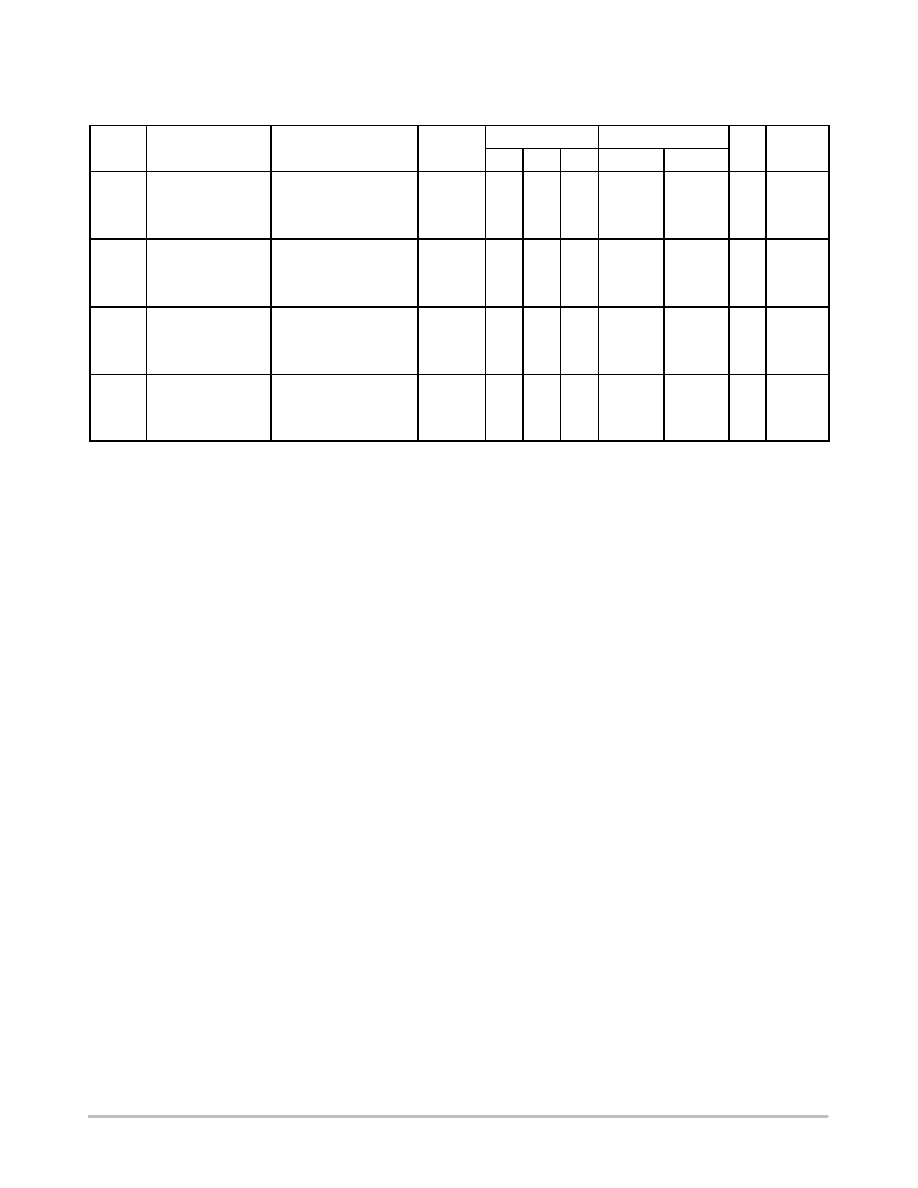
DC ELECTRICAL CHARACTERISTICS
V
CC
T
A
= +25
5
C
T
A
= -40
5
C to +85
5
C
Symbol
Parameter
Test Conditions
V
CC
(V)
Min
Typ
Max
Min
Max
Unit
V
IH
HIGH Level
Input Voltage
1.65-1.95
2.3-5.5
0.75 V
CC
0.7 V
CC
V
V
IL
LOW Level
Input Voltage
1.65-1.95
2.3-5.5
0.25 V
CC
0.3 V
CC
V
I
IN
Input Leakage Current
0
v
V
IN
v
5.5 V
0-5.5
"
0.05
"
0.1
"
1
m
A
I
OFF
OFF State Leakage
Current
0
v
A, B
v
V
CC
1.65-5.5
"
0.05
"
0.1
"
1
m
A
R
ON
Switch On Resistance
(Note 3)
V
IN
= 0 V, I
O
= 30 mA
V
IN
= 2.4 V, I
O
= -30 mA
V
IN
= 4.5 V, I
O
= -30 mA
4.5
3.0
5.0
7.0
7.0
12
15
W
V
IN
= 0 V, I
O
= 24 mA
V
IN
= 3 V, I
O
= -24 mA
3.0
4.0
10
9.0
20
W
V
IN
= 0 V, I
O
= 8 mA
V
IN
= 2.3 V, I
O
= -8 mA
2.3
5.0
13
12
30
W
V
IN
= 0 V, I
O
= 4 mA
V
IN
= 1.65 V, I
O
= -4 mA
1.65
6.5
17
20
50
W
I
CC
Quiescent Supply
Current
All Channels ON or
OFF
V
IN
= V
CC
or GND
I
OUT
= 0
5.5
1.0
10
m
A
Analog Signal Range
V
CC
0
V
CC
0
V
CC
V
R
RANGE
On Resistance
Over Signal Range
(Note 3) (Note 7)
I
A
= -30 mA, 0
v
V
Bn
v
V
CC
I
A
= -24 mA, 0
v
V
Bn
v
V
CC
I
A
= -8 mA, 0
v
V
Bn
v
V
CC
I
A
= -4 mA, 0
v
V
Bn
v
V
CC
4.5
3.0
2.3
1.65
25
50
100
300
W
D
R
ON
On Resistance Match
Between Channels
(Note 3) (Note 4)
(Note 5)
I
A
= -30 mA, V
Bn
= 3.15
I
A
= -24 mA, V
Bn
= 2.1
I
A
= -8 mA, V
Bn
= 1.6
I
A
= -4 mA, V
Bn
= 1.15
4.5
3.0
2.3
1.65
0.15
0.2
0.5
0.5
W
R
flat
On Resistance
Flatness (Note 3)
(Note 4) (Note 6)
I
A
= -30 mA, 0
v
V
Bn
v
V
CC
I
A
= -24 mA, 0
v
V
Bn
v
V
CC
I
A
= -8 mA, 0
v
V
Bn
v
V
CC
I
A
= -4 mA, 0
v
V
Bn
v
V
CC
5.0
3.3
2.5
1.8
6.0
12
28
125
W
3. Measured by the voltage drop between A and B pins at the indicated current through the switch. On Resistance is determined by the lower
of the voltages on the two (A or B Ports).
4. Parameter is characterized but not tested in production.
5.
D
R
ON
= R
ON
max - R
ON
min measured at identical V
CC
, temperature and voltage levels.
6. Flatness is defined as the difference between the maximum and minimum value of On Resistance over the specified range of conditions.
7. Guaranteed by Design.

NLASB3157
http://onsemi.com
4
AC ELECTRICAL CHARACTERISTICS
V
CC
T
A
= +25
5
C
T
A
= -40
5
C to +85
5
C
Figure
Symbol
Parameter
Test Conditions
V
CC
(V)
Min
Typ
Max
Min
Max
Unit
Figure
Number
t
PHL
t
PLH
Propagation Delay
Bus to Bus (Note 9)
V
I
= OPEN
1.65-1.95
2.3-2.7
3.0-3.6
4.5-5.5
1.2
0.8
0.3
ns
Figures
2, 3
t
PZL
t
PZH
Output Enable Time
Turn On Time
(A to B
n
)
V
I
= 2
V
CC
for t
PZL
V
I
= 0 V for t
PZH
1.65-1.95
2.3-2.7
3.0-3.6
4.5-5.5
23
13
6.9
5.2
7.0
3.5
2.5
1.7
24
14
7.6
5.7
ns
Figures
2, 3
t
PLZ
t
PHZ
Output Disable Time
Turn Off Time
(A Port to B Port)
V
I
= 2
V
CC
for t
PLZ
V
I
= 0 V for t
PHZ
1.65-1.95
2.3-2.7
3.0-3.6
4.5-5.5
12.5
7.0
5.0
3.5
3.0
2.0
1.5
0.8
13
7.5
5.3
3.8
ns
Figures
2, 3
t
B-M
Break Before Make
Time (Note 8)
1.65-1.95
2.3-2.7
3.0-3.6
4.5-5.5
0.5
0.5
0.5
0.5
ns
Figure 4
Q
Charge Injection
(Note 8)
C
L
= 0.1 nF, V
GEN
= 0 V
R
GEN
= 0
W
5.0
3.3
7.0
3.0
pC
Figure 5
OIRR
Off Isolation (Note 10)
R
L
= 50
W
f = 10 MHz
1.65-5.5
-57
dB
Figure 6
Xtalk
Crosstalk
R
L
= 50
W
f = 10 MHz
1.65-5.5
-54
dB
Figure 7
BW
-3 dB Bandwidth
R
L
= 50
W
1.65-5.5
250
MHz
Figure 10
THD
Total Harmonic
Distortion (Note 8)
R
L
= 600
W
0.5 V
P-P
f = 600 Hz to 20 kHz
5.0
0.011
%
CAPACITANCE
(Note 11)
Symbol
Parameter
Test Conditions
Typ
Max
Unit
Figure
Number
C
IN
Select Pin Input Capacitance
V
CC
= 0 V
2.3
pF
C
IO-B
B Port Off Capacitance
V
CC
= 5.0 V
6.5
pF
Figure 8
C
IOA-ON
A Port Capacitance when Switch is Enabled
V
CC
= 5.0 V
18.5
pF
Figure 9
8. Guaranteed by Design.
9. This parameter is guaranteed by design but not tested. The bus switch contributes no propagation delay other than the RC delay of the On
Resistance of the switch and the 50 pF load capacitance, when driven by an ideal voltage source (zero output impedance).
10. Off Isolation = 20 log
10
[V
A
/V
Bn
].
11. T
A
= +25
∞
C, f = 1 MHz, Capacitance is characterized but not tested in production.
NLASB3157
http://onsemi.com
5
APPENDIX A
DC ELECTRICAL EXTENDED AUTOMOTIVE TEMPERATURE RANGE CHARACTERISTICS
V
CC
T
A
= +25
5
C
T
A
= -55
5
C to +125
5
C
Symbol
Parameter
Test Conditions
V
CC
(V)
Min
Typ
Max
Min
Max
Unit
V
IH
HIGH Level
Input Voltage
1.65-1.95
2.3-5.5
0.75 V
CC
0.7 V
CC
V
V
IL
LOW Level
Input Voltage
1.65-1.95
2.3-5.5
0.25 V
CC
0.3 V
CC
V
I
IN
Input Leakage Current
0
v
V
IN
v
5.5 V
0-5.5
"
0.05
"
0.1
"
1
m
A
I
OFF
OFF State Leakage
Current
0
v
A, B
v
V
CC
1.65-5.5
"
0.05
"
0.1
"
1
m
A
R
ON
Switch On Resistance
(Note 12)
V
IN
= 0 V, I
O
= 30 mA
V
IN
= 2.4 V, I
O
= -30 mA
V
IN
= 4.5 V, I
O
= -30 mA
4.5
3.0
5.0
7.0
8.5
13.0
15.0
W
V
IN
= 0 V, I
O
= 24 mA
V
IN
= 3 V, I
O
= -24 mA
3.0
4.0
10
11
20
V
IN
= 0 V, I
O
= 8 mA
V
IN
= 2.3 V, I
O
= -8 mA
2.3
5.0
13
12
30
V
IN
= 0 V, I
O
= 4 mA
V
IN
= 1.65 V, I
O
= -4 mA
1.65
6.5
17
20
50
I
CC
Quiescent Supply
Current
All Channels ON or
OFF
V
IN
= V
CC
or GND
I
OUT
= 0
5.5
1.0
10
m
A
Analog Signal Range
V
CC
0
V
CC
0
V
CC
V
R
RANGE
On Resistance
Over Signal Range
(Note 12) (Note 14)
I
A
= -30 mA, 0
v
V
Bn
v
V
CC
I
A
= -24 mA, 0
v
V
Bn
v
V
CC
I
A
= -8 mA, 0
v
V
Bn
v
V
CC
I
A
= -4 mA, 0
v
V
Bn
v
V
CC
4.5
3.0
2.3
1.65
25
50
100
300
W
12. Measured by the voltage drop between A and B pins at the indicated current through the switch. On Resistance is determined by the lower
of the voltages on the two (A or B Ports).
13. Flatness is defined as the difference between the maximum and minimum value of On Resistance over the specified range of conditions.
14. Guaranteed by Design.
* For
D
R
ON
, R
FLAT
, Q, OIRR, Xtalk, BW, THD, and CIN see -40
5
C to 85
5
C section.
NLASB3157
http://onsemi.com
6
APPENDIX A
AC ELECTRICAL EXTENDED AUTOMOTIVE TEMPERATURE RANGE CHARACTERISTICS
V
CC
T
A
= +25
5
C
T
A
= -55
5
C to +125
5
C
Figure
Symbol
Parameter
Test Conditions
V
CC
(V)
Min
Typ
Max
Min
Max
Unit
Figure
Number
t
PHL
t
PLH
Propagation Delay
Bus to Bus (Note 16)
V
I
= OPEN
1.65-1.95
2.3-2.7
3.0-3.6
4.5-5.5
1.2
0.8
0.3
ns
Figures
2, 3
t
PZL
t
PZH
Output Enable Time
Turn On Time
(A to B
n
)
V
I
= 2
V
CC
for t
PZL
V
I
= 0 V for t
PZH
1.65-1.95
2.3-2.7
3.0-3.6
4.5-5.5
23
13
6.9
5.2
7.0
3.5
2.5
1.7
24
14
9.0
7.0
ns
Figures
2, 3
t
PLZ
t
PHZ
Output Disable Time
Turn Off Time
(A Port to B Port)
V
I
= 2
V
CC
for t
PLZ
V
I
= 0 V for t
PHZ
1.65-1.95
2.3-2.7
3.0-3.6
4.5-5.5
12.5
7.0
5.0
3.5
3.0
2.0
1.5
0.8
13
7.5
6.5
5.0
ns
Figures
2, 3
t
B-M
Break Before Make
Time (Note 15)
1.65-1.95
2.3-2.7
3.0-3.6
4.5-5.5
0.5
0.5
0.5
0.5
ns
Figure 4
15. Guaranteed by Design.
16. This parameter is guaranteed by design but not tested. The bus switch contributes no propagation delay other than the RC delay of the On
Resistance of the switch and the 50 pF load capacitance, when driven by an ideal voltage source (zero output impedance).
* For
D
R
ON
, R
FLAT
, Q, OIRR, Xtalk, BW, THD, and CIN see -40
5
C to 85
5
C section.
NLASB3157
http://onsemi.com
7
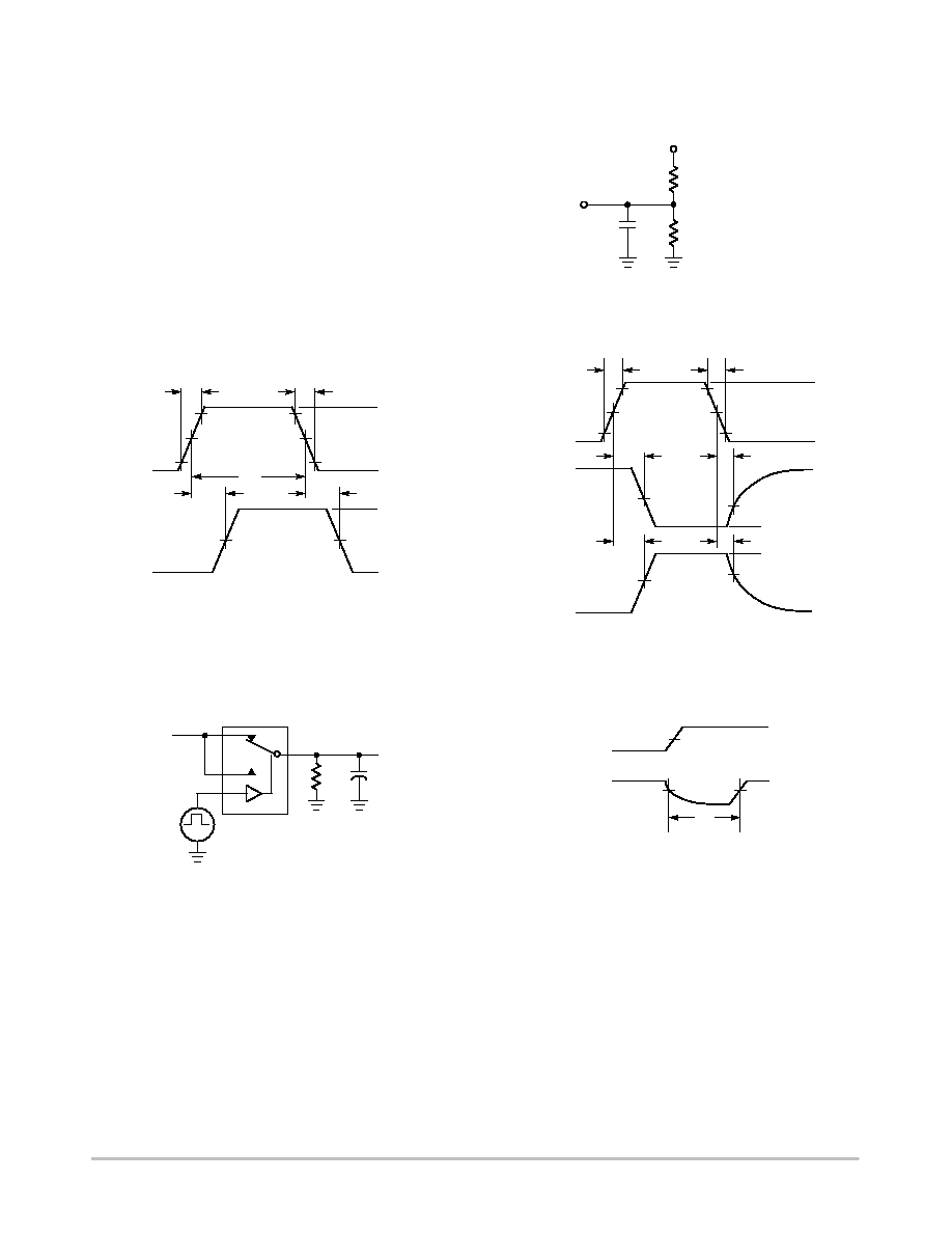
t
W
V
CC
GND
V
OH
V
OL
50%
10%
10%
50%
50%
90%
90%
t
f
= 2.5 ns
t
r
= 2.5 ns
SWITCH
INPUT
OUTPUT
50%
t
PHL
t
PLH
V
CC
GND
V
TRI
50%
10%
10%
50%
50%
90%
90%
t
f
= 2.5 ns
t
r
= 2.5 ns
SELECT
INPUT
OUTPUT
t
PZL
V
TRI
OUTPUT
50%
t
PZH
V
OL
V
OH
t
PHZ
t
PLZ
V
OL
+ 0.3 V
V
OH
- 0.3 V
NOTE: Input driven by 50
W
source terminated in 50
W
NOTE: C
L
includes load and stray capacitance
NOTE: Input PRR = 1.0 MHz; t
W
= 500 ns
V
I
RD
RU
C
L
FROM
OUTPUT
UNDER
TEST
Figure 2. AC Test Circuit
Figure 3. AC Waveforms
Figure 4. Break Before Make Interval Timing
LOGIC
INPUT
V
OUT
t
D
0.9
◊
V
OUT
R
L
C
L
V
OUT
V
IN
LOGIC
INPUT
A
S
B
0
B
1
AC LOADING AND WAVEFORMS
NLASB3157
http://onsemi.com
8
Figure 5. Charge Injection Test
R
L
1 M
W
C
L
100 pF
V
OUT
LOGIC
INPUT
A
S
B
N
R
GEN
V
GE
Q = (
D
V
OUT
)(C
L
)
D
V
OUT
ON
OFF
OFF
V
OUT
LOGIC
INPUT
Figure 6. Off Isolation
Figure 7. Crosstalk
S
B
N
LOGIC INPUT
0 V or V
IH
10 nF
V
CC
Analyzer
A
GND
50
W
50
W
S
B
0
10 nF
V
CC
Analyzer
A
GND
50
W
Signal
Generator
0 dBm
50
W
B
1
Figure 8. Channel Off Capacitance
Figure 9. Channel On Capacitance
Figure 10. Bandwidth
S
B
N
10 nF
V
CC
A
GND
Signal
Generator
0 dBm
50
W
LOGIC INPUT
0 V or V
CC
S
B
N
LOGIC INPUT
0 V or V
CC
10 nF
V
CC
A
GND
Capacitance
Meter
S
B
N
LOGIC INPUT
0 V or V
CC
10 nF
V
CC
A
GND
Capacitance
Meter
f = 1 MHz
f = 1 MHz
AC LOADING AND WAVEFORMS
NLASB3157
http://onsemi.com
9
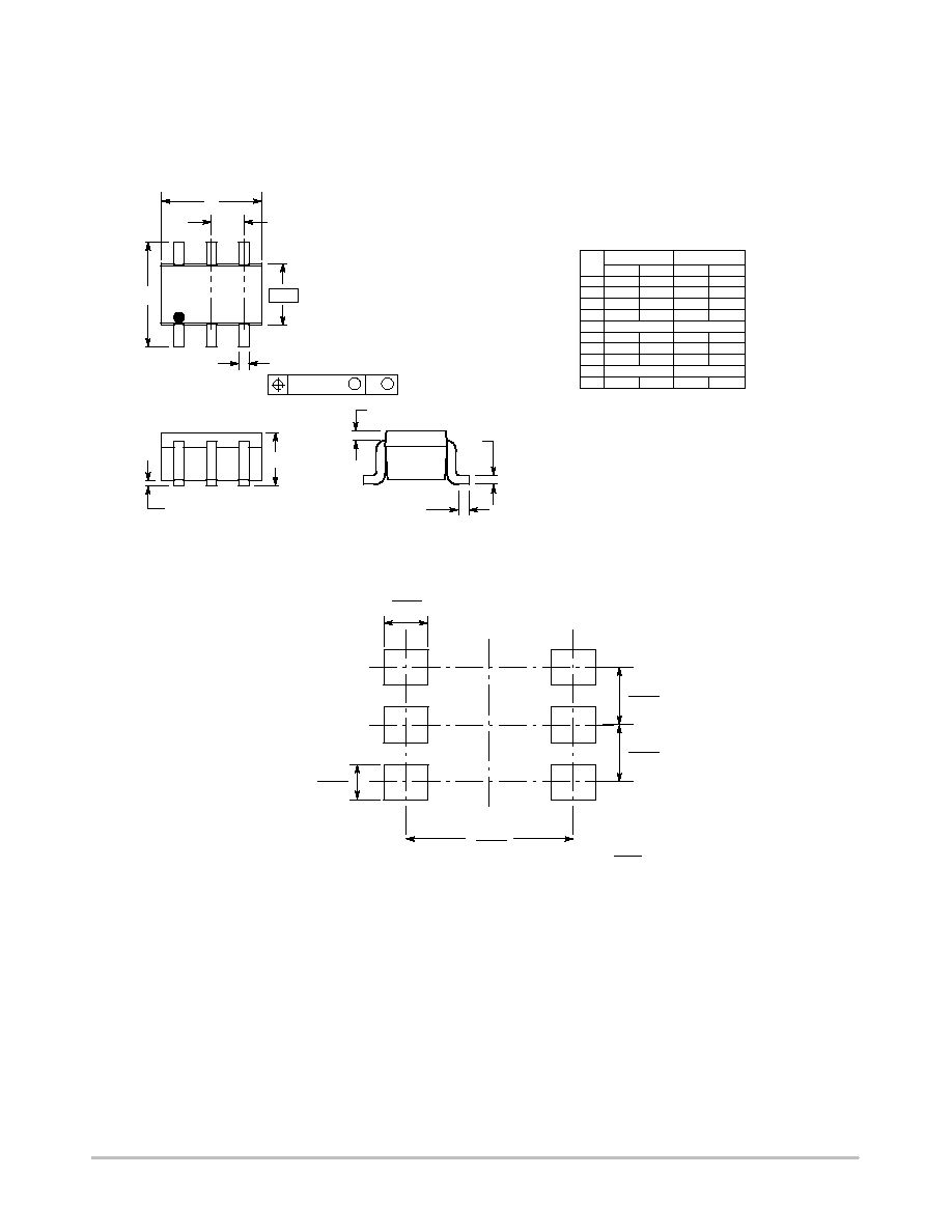
PACKAGE DIMENSIONS
SC-88/SOT-363/SC-70
DF SUFFIX
CASE 419B-02
ISSUE U
*For additional information on our Pb-Free strategy and soldering
details, please download the ON Semiconductor Soldering and
Mounting Techniques Reference Manual, SOLDERRM/D.
SOLDERING FOOTPRINT*
NOTES:
1. DIMENSIONING AND TOLERANCING PER ANSI
Y14.5M, 1982.
2. CONTROLLING DIMENSION: INCH.
3. 419B-01 OBSOLETE, NEW STANDARD 419B-02.
DIM
A
MIN
MAX
MIN
MAX
MILLIMETERS
1.80
2.20
0.071
0.087
INCHES
B
1.15
1.35
0.045
0.053
C
0.80
1.10
0.031
0.043
D
0.10
0.30
0.004
0.012
G
0.65 BSC
0.026 BSC
H
---
0.10
---
0.004
J
0.10
0.25
0.004
0.010
K
0.10
0.30
0.004
0.012
N
0.20 REF
0.008 REF
S
2.00
2.20
0.079
0.087
B
0.2 (0.008)
M
M
1
2
3
A
G
S
H
C
N
J
K
6
5
4
-B-
D
6 PL
mm
inches
SCALE 20:1
0.65
0.025
0.65
0.025
0.50
0.0197
0.40
0.0157
1.9
0.0748

NLASB3157
http://onsemi.com
10
ON Semiconductor and are registered trademarks of Semiconductor Components Industries, LLC (SCILLC). SCILLC reserves the right to make changes without further notice
to any products herein. SCILLC makes no warranty, representation or guarantee regarding the suitability of its products for any particular purpose, nor does SCILLC assume any
liability arising out of the application or use of any product or circuit, and specifically disclaims any and all liability, including without limitation special, consequential or incidental
damages. "Typical" parameters which may be provided in SCILLC data sheets and/or specifications can and do vary in different applications and actual performance may vary over
time. All operating parameters, including "Typicals" must be validated for each customer application by customer's technical experts. SCILLC does not convey any license under
its patent rights nor the rights of others. SCILLC products are not designed, intended, or authorized for use as components in systems intended for surgical implant into the body,
or other applications intended to support or sustain life, or for any other application in which the failure of the SCILLC product could create a situation where personal injury or death
may occur. Should Buyer purchase or use SCILLC products for any such unintended or unauthorized application, Buyer shall indemnify and hold SCILLC and its officers, employees,
subsidiaries, affiliates, and distributors harmless against all claims, costs, damages, and expenses, and reasonable attorney fees arising out of, directly or indirectly, any claim of
personal injury or death associated with such unintended or unauthorized use, even if such claim alleges that SCILLC was negligent regarding the design or manufacture of the part.
SCILLC is an Equal Opportunity/Affirmative Action Employer. This literature is subject to all applicable copyright laws and is not for resale in any manner.
PUBLICATION ORDERING INFORMATION
N. American Technical Support: 800-282-9855 Toll Free
USA/Canada
Japan: ON Semiconductor, Japan Customer Focus Center
2-9-1 Kamimeguro, Meguro-ku, Tokyo, Japan 153-0051
Phone: 81-3-5773-3850
NLASB3157/D
LITERATURE FULFILLMENT:
Literature Distribution Center for ON Semiconductor
P.O. Box 5163, Denver, Colorado 80217 USA
Phone: 303-675-2175 or 800-344-3860 Toll Free USA/Canada
Fax: 303-675-2176 or 800-344-3867 Toll Free USA/Canada
Email: orderlit@onsemi.com
ON Semiconductor Website: http://onsemi.com
Order Literature: http://www.onsemi.com/litorder
For additional information, please contact your
local Sales Representative.