
©
Semiconductor Components Industries, LLC, 2003
February, 2003 - Rev. 2
1
Publication Order Number:
NSBC114EPDXV6/D
NSBC114EPDXV6T1,
NSBC114EPDXV6T5
Preferred Devices
Dual Bias Resistor
Transistors
NPN and PNP Silicon Surface Mount
Transistors with Monolithic Bias
Resistor Network
The BRT (Bias Resistor Transistor) contains a single transistor with
a monolithic bias network consisting of two resistors; a series base
resistor and a base-emitter resistor. These digital transistors are
designed to replace a single device and its external resistor bias
network. The BRT eliminates these individual components by
integrating them into a single device. In the NSBC114EPDXV6T1
series, two complementary BRT devices are housed in the SOT-563
package which is ideal for low power surface mount applications
where board space is at a premium.
∑
Simplifies Circuit Design
∑
Reduces Board Space
∑
Reduces Component Count
∑
Available in 8 mm, 7 inch Tape and Reel
∑
Lead Free Solder Plating
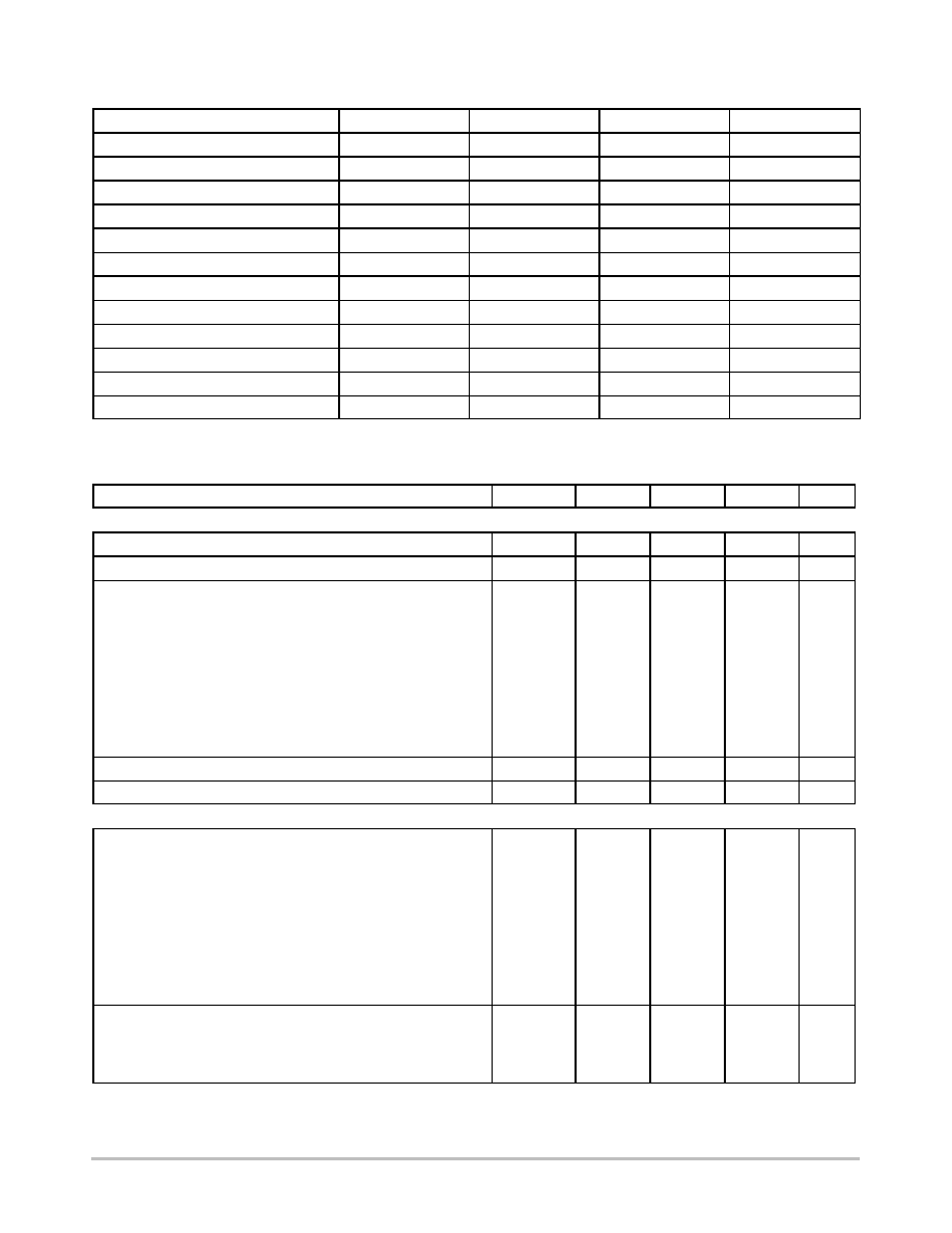
MAXIMUM RATINGS
(T
A
= 25
∞
C unless otherwise noted, common for Q
1
and Q
2
, - minus sign for Q
1
(PNP) omitted)
Rating
Symbol
Value
Unit
Collector-Base Voltage
V
CBO
50
Vdc
Collector-Emitter Voltage
V
CEO
50
Vdc
Collector Current
I
C
100
mAdc
THERMAL CHARACTERISTICS
Characteristic
(One Junction Heated)
Symbol
Max
Unit
Total Device Dissipation
T
A
= 25
∞
C
Derate above 25
∞
C
P
D
357
(Note 1)
2.9
(Note 1)
mW
mW/
∞
C
Thermal Resistance Junction-to-Ambient
R
q
JA
350
(Note 1)
∞
C/W
Characteristic
(Both Junctions Heated)
Symbol
Max
Unit
Total Device Dissipation
T
A
= 25
∞
C
Derate above 25
∞
C
P
D
500
(Note 1)
4.0
(Note 1)
mW
mW/
∞
C
Thermal Resistance Junction-to-Ambient
R
q
JA
250
(Note 1)
∞
C/W
Junction and Storage Temperature
T
J
, T
stg
- 55 to
+150
∞
C
1. FR-4 @ Minimum Pad
Preferred devices are recommended choices for future use
and best overall value.
DEVICE MARKING INFORMATION
See specific marking information in the device marking table
on page 2 of this data sheet.
Q
1
R
1
R
2
R
2
R
1
Q
2
(1)
(2)
(3)
(4)
(5)
(6)
http://onsemi.com
SOT-563
CASE 463A
PLASTIC
1
2
3
6
5 4
xx = Specific Device Code
(see table on page 2)
D
= Date Code
MARKING DIAGRAM
xx D
Device
Package
Shipping
ORDERING INFORMATION
NSBC114EPDXV6T1 SOT-563
4 mm pitch
4000/Tape & Reel
NSBC114EPDXV6T5 SOT-563
2 mm pitch
8000/Tape & Reel
NSBC114EPDXV6T1, NSBC114EPDXV6T5
http://onsemi.com
2
DEVICE MARKING AND RESISTOR VALUES
Device
Package
Marking
R1 (k
W
)
R2 (k
W
)
NSBC114EPDXV6T1
SOT-563
11
10
10
NSBC124EPDXV6T1
SOT-563
12
22
22
NSBC144EPDXV6T1
SOT-563
13
47
47
NSBC114YPDXV6T1
SOT-563
14
10
47
NSBC114TPDXV6T1 (Note 2, 4)
SOT-563
15
10
NSBC143TPDXV6T1 (Note 2, 4)
SOT-563
16
4.7
NSBC113EPDXV6T1 (Note 2, 4)
SOT-563
30
1.0
1.0
NSBC123EPDXV6T1 (Note 2, 4)
SOT-563
31
2.2
2.2
NSBC143EPDXV6T1 (Note 2, 4)
SOT-563
32
4.7
4.7
NSBC143ZPDXV6T1 (Note 2, 4)
SOT-563
33
4.7
47
NSBC124XPDXV6T1 (Note 2, 4)
SOT-563
34
22
47
NSBC123JPDXV6T1 (Note 2)
SOT-563
35
2.2
47
ELECTRICAL CHARACTERISTICS
(T
A
= 25
∞
C unless otherwise noted, common for Q
1
and Q
2
, - minus sign for Q
1
(PNP) omitted)
Characteristic
Symbol
Min
Typ
Max
Unit
OFF CHARACTERISTICS
Collector-Base Cutoff Current (V
CB
= 50 V, I
E
= 0)
I
CBO
-
-
100
nAdc
Collector-Emitter Cutoff Current (V
CE
= 50 V, I
B
= 0)
I
CEO
-
-
500
nAdc
Emitter-Base Cutoff Current
NSBC114EPDXV6T1
(V
EB
= 6.0 V, I
C
= 0)
NSBC124EPDXV6T1
NSBC144EPDXV6T1
NSBC114YPDXV6T1
NSBC114TPDXV6T1
NSBC143TPDXV6T1
NSBC113EPDXV6T1
NSBC123EPDXV6T1
NSBC143EPDXV6T1
NSBC143ZPDXV6T1
NSBC124XPDXV6T1
NSBC123JPDXV6T1
I
EBO
-
-
-
-
-
-
-
-
-
-
-
-
-
-
-
-
-
-
-
-
-
-
-
-
0.5
0.2
0.1
0.2
0.9
1.9
4.3
2.3
1.5
0.18
0.13
0.2
mAdc
Collector-Base Breakdown Voltage (I
C
= 10
m
A, I
E
= 0)
V
(BR)CBO
50
-
-
Vdc
Collector-Emitter Breakdown Voltage (Note 3) (I
C
= 2.0 mA, I
B
= 0)
V
(BR)CEO
50
-
-
Vdc
ON CHARACTERISTICS (Note 3)
DC Current Gain
NSBC114EPDXV6T1
(V
CE
= 10 V, I
C
= 5.0 mA)
NSBC124EPDXV6T1
NSBC144EPDXV6T1
NSBC114YPDXV6T1
NSBC114TPDXV6T1
NSBC143TPDXV6T1
NSBC113EPDXV6T1
NSBC123EPDXV6T1
NSBC143EPDXV6T1
NSBC143ZPDXV6T1
NSBC124XPDXV6T1
NSBC123JPDXV6T1
h
FE
35
60
80
80
160
160
3.0
8.0
15
80
80
80
60
100
140
140
350
350
5.0
15
30
200
150
140
-
-
-
-
-
-
-
-
-
-
-
-
Collector-Emitter Saturation Voltage
(I
C
= 10 mA, I
B
= 0.3 mA)
(I
C
= 10 mA, I
B
= 5 mA) NSBC113EPDXV6T1/NSBC123EPDXV6T1
(I
C
= 10 mA, I
B
= 1 mA)
NSBC114TPDXV6T1/NSBC143TPDXV6T1
NSBC143EPDXV6T1/NSBC143ZPDXV6T1/NSBC124XPDXV6T1
V
CE(sat)
-
-
0.25
Vdc
2. New resistor combinations. Updated curves to follow in subsequent data sheets.
3. Pulse Test: Pulse Width < 300
m
s, Duty Cycle < 2.0%
4. Available upon request.

NSBC114EPDXV6T1, NSBC114EPDXV6T5
http://onsemi.com
3
ELECTRICAL CHARACTERISTICS
(T
A
= 25
∞
C unless otherwise noted, common for Q
1
and Q
2
, - minus sign for Q
1
(PNP) omitted)
Characteristic
Unit
Max
Typ
Min
Symbol
ON CHARACTERISTICS (Note 3)
Output Voltage (on)
(V
CC
= 5.0 V, V
B
= 2.5 V, R
L
= 1.0 k
W
)
NSBC114EPDXV6T1
NSBC124EPDXV6T1
NSBC114YPDXV6T1
NSBC114TPDXV6T1
NSBC143TPDXV6T1
NSBC113EPDXV6T1
NSBC123EPDXV6T1
NSBC143EPDXV6T1
NSBC143ZPDXV6T1
NSBC124XPDXV6T1
NSBC123JPDXV6T1
(V
CC
= 5.0 V, V
B
= 3.5 V, R
L
= 1.0 k
W
)
NSBC144EPDXV6T1
V
OL
-
-
-
-
-
-
-
-
-
-
-
-
-
-
-
-
-
-
-
-
-
-
-
-
0.2
0.2
0.2
0.2
0.2
0.2
0.2
0.2
0.2
0.2
0.2
0.2
Vdc
Output Voltage (off)
(V
CC
= 5.0 V, V
B
= 0.5 V, R
L
= 1.0 k
W
)
(V
CC
= 5.0 V, V
B
= 0.050 V, R
L
= 1.0 k
W
)
NSBC113EPDXV6T1
(V
CC
= 5.0 V, V
B
= 0.25 V, R
L
= 1.0 k
W
)
NSBC114TPDXV6T1
NSBC143TPDXV6T1
NSBC143ZPDXV6T1
V
OH
4.9
-
-
Vdc
Input Resistor
NSBC114EPDXV6T1
NSBC124EPDXV6T1
NSBC144EPDXV6T1
NSBC114YPDXV6T1
NSBC114TPDXV6T1
NSBC143TPDXV6T1
NSBC113EPDXV6T1
NSBC123EPDXV6T1
NSBC143EPDXV6T1
NSBC143ZPDXV6T1
NSBC124XPDXV6T1
NSBC123JPDXV6T1
R1
7.0
15.4
32.9
7.0
7.0
3.3
0.7
1.5
3.3
3.3
15.4
1.54
10
22
47
10
10
4.7
1.0
2.2
4.7
4.7
22
2.2
13
28.6
61.1
13
13
6.1
1.3
2.9
6.1
6.1
28.6
2.86
k
W
Resistor Ratio
NSBC114EPDXV6T1/NSBC124EPDXV6T1/NSBC144EPDXV6T1
NSBC114YPDXV6T1
NSBC114TPDXV6T1/NSBC143TPDXV6T1
NSBC113EPDXV6T1/NSBC123EPDXV6T1/NSBC143EPDXV6T1
NSBC143ZPDXV6T1
NSBC124XPDXV6T1
NSBC123JPDXV6T1
R1/R2
0.8
0.17
-
0.8
0.055
0.38
0.038
1.0
0.21
-
1.0
0.1
0.47
0.047
1.2
0.25
-
1.2
0.185
0.56
0.056
2. New resistor combinations. Updated curves to follow in subsequent data sheets.
3. Pulse Test: Pulse Width < 300
m
s, Duty Cycle < 2.0%
4. Available upon request.
NSBC114EPDXV6T1, NSBC114EPDXV6T5
http://onsemi.com
4
Figure 1. Derating Curve
300
200
150
100
50
0
- 50
0
50
100
150
T
A
, AMBIENT TEMPERATURE (
∞
C)
R
q
JA
= 490
∞
C/W
250
P
D
, POWER DISSIP
A
TION (mW)
NSBC114EPDXV6T1, NSBC114EPDXV6T5
http://onsemi.com
5
TYPICAL ELECTRICAL CHARACTERISTICS - NSBC114EPDXV6T1 NPN TRANSISTOR
V in
, INPUT
VOL
T
AGE (VOL
TS)
I C
, COLLECT
OR CURRENT
(mA)
h FE
, DC CURRENT
GAIN (NORMALIZED)
Figure 2. V
CE(sat)
versus I
C
10
0
20
30
I
C
, COLLECTOR CURRENT (mA)
10
1
0.1
T
A
= -25
∞
C
75
∞
C
25
∞
C
40
50
Figure 3. DC Current Gain
Figure 4. Output Capacitance
1
0.1
0.01
0.001
0
20
40
50
I
C
, COLLECTOR CURRENT (mA)
V CE(sat)
, MAXIMUM COLLECT
OR VOL
T
AGE (VOL
TS)
1000
100
10
1
10
100
I
C
, COLLECTOR CURRENT (mA)
T
A
= 75
∞
C
25
∞
C
-25
∞
C
T
A
= -25
∞
C
25
∞
C
Figure 5. Output Current versus Input Voltage
75
∞
C
25
∞
C
T
A
= -25
∞
C
100
10
1
0.1
0.01
0.001
0
1
2
3
4
V
in
, INPUT VOLTAGE (VOLTS)
5
6
7
8
9
10
Figure 6. Input Voltage versus Output Current
50
0
10
20
30
40
4
3
1
2
0
V
R
, REVERSE BIAS VOLTAGE (VOLTS)
C ob
, CAP
ACIT
ANCE (pF)
75
∞
C
V
CE
= 10 V
f = 1 MHz
I
E
= 0 V
T
A
= 25
∞
C
V
O
= 5 V
V
O
= 0.2 V
I
C
/I
B
= 10

NSBC114EPDXV6T1, NSBC114EPDXV6T5
http://onsemi.com
6
TYPICAL ELECTRICAL CHARACTERISTICS - NSBC114EPDXV6T1 PNP TRANSISTOR
V in
, INPUT
VOL
T
AGE (VOL
TS)
I C
, COLLECT
OR CURRENT
(mA)
h FE
, DC CURRENT
GAIN (NORMALIZED)
Figure 7. V
CE(sat)
versus I
C
100
10
1
0.1
0.01
0.001
0
V
in
, INPUT VOLTAGE (VOLTS)
T
A
= -25
∞
C
25
∞
C
1
2
3
4
5
6
7
8
9
10
Figure 8. DC Current Gain
Figure 9. Output Capacitance
Figure 10. Output Current versus Input
Voltage
Figure 11. Input Voltage versus Output Current
0.01
20
I
C
, COLLECTOR CURRENT (mA)
V CE(sat)
, MAXIMUM COLLECT
OR VOL
T
AGE (VOL
T
S
0.1
1
0
40
50
1000
1
10
100
I
C
, COLLECTOR CURRENT (mA)
T
A
= 75
∞
C
-25
∞
C
100
10
0
I
C
, COLLECTOR CURRENT (mA)
0.1
1
10
100
10
20
30
40
50
T
A
= -25
∞
C
25
∞
C
75
∞
C
75
∞
C
I
C
/I
B
= 10
50
0
10
20
30
40
4
3
1
2
V
R
, REVERSE BIAS VOLTAGE (VOLTS)
C ob
, CAP
ACIT
ANCE (pF)
0
T
A
= -25
∞
C
25
∞
C
75
∞
C
25
∞
C
V
CE
= 10 V
f = 1 MHz
l
E
= 0 V
T
A
= 25
∞
C
V
O
= 5 V
V
O
= 0.2 V
NSBC114EPDXV6T1, NSBC114EPDXV6T5
http://onsemi.com
7
TYPICAL ELECTRICAL CHARACTERISTICS - NSBC124EPDXV6T1 NPN TRANSISTOR
V in
, INPUT
VOL
T
AGE (VOL
TS)
I C
, COLLECT
OR CURRENT
(mA)
h FE
, DC CURRENT
GAIN (NORMALIZED)
Figure 12. V
CE(sat)
versus I
C
Figure 13. DC Current Gain
Figure 14. Output Capacitance
Figure 15. Output Current versus Input Voltage
1000
10
I
C
, COLLECTOR CURRENT (mA)
T
A
= 75
∞
C
25
∞
C
-25
∞
C
100
10
1
100
75
∞
C
25
∞
C
100
0
V
in
, INPUT VOLTAGE (VOLTS)
10
1
0.1
0.01
0.001
2
4
6
8
10
T
A
= -25
∞
C
0
I
C
, COLLECTOR CURRENT (mA)
100
T
A
= -25
∞
C
75
∞
C
10
1
0.1
10
20
30
40
50
25
∞
C
Figure 16. Input Voltage versus Output
Current
0.001
V CE(sat)
, MAXIMUM COLLECT
OR VOL
T
AGE (VOL
TS
)
T
A
= -25
∞
C
75
∞
C
25
∞
C
0.01
0.1
1
40
I
C
, COLLECTOR CURRENT (mA)
0
20
50
50
0
10
20
30
40
4
3
2
1
0
V
R
, REVERSE BIAS VOLTAGE (VOLTS)
C ob
, CAP
ACIT
ANCE (pF)
I
C
/I
B
= 10
V
CE
= 10 V
f = 1 MHz
I
E
= 0 V
T
A
= 25
∞
C
V
O
= 5 V
V
O
= 0.2 V

NSBC114EPDXV6T1, NSBC114EPDXV6T5
http://onsemi.com
8
TYPICAL ELECTRICAL CHARACTERISTICS - NSBC124EPDXV6T1 PNP TRANSISTOR
V in
, INPUT
VOL
T
AGE (VOL
TS)
I C
, COLLECT
OR CURRENT
(mA)
h FE
, DC CURRENT
GAIN (NORMALIZED)
Figure 17. V
CE(sat)
versus I
C
Figure 18. DC Current Gain
1000
10
I
C
, COLLECTOR CURRENT (mA)
100
10
1
100
Figure 19. Output Capacitance
I
C
, COLLECTOR CURRENT (mA)
0
10
20
30
V
O
= 0.2 V
T
A
= -25
∞
C
75
∞
C
100
10
1
0.1
40
50
Figure 20. Output Current versus Input Voltage
100
10
1
0.1
0.01
0.001 0 1
2
3
4
V
in
, INPUT VOLTAGE (VOLTS)
5
6
7
8
9
10
Figure 21. Input Voltage versus Output Current
0.01
V CE(sat)
, MAXIMUM COLLECT
OR VOL
T
AGE (VOL
TS)
0.1
1
10
40
I
C
, COLLECTOR CURRENT (mA)
0
20
50
75
∞
C
25
∞
C
T
A
= -25
∞
C
50
0
10
20
30
40
4
3
2
1
0
V
R
, REVERSE BIAS VOLTAGE (VOLTS)
C ob
, CAP
ACIT
ANCE (pF)
25
∞
C
I
C
/I
B
= 10
25
∞
C
-25
∞
C
V
CE
= 10 V
T
A
= 75
∞
C
f = 1 MHz
l
E
= 0 V
T
A
= 25
∞
C
75
∞
C
25
∞
C
T
A
= -25
∞
C
V
O
= 5 V

NSBC114EPDXV6T1, NSBC114EPDXV6T5
http://onsemi.com
9
TYPICAL ELECTRICAL CHARACTERISTICS - NSBC144EPDXV6T1 NPN TRANSISTOR
V in
, INPUT
VOL
T
AGE (VOL
TS)
I C
, COLLECT
OR CURRENT
(mA)
h FE
, DC CURRENT
GAIN (NORMALIZED)
Figure 22. V
CE(sat)
versus I
C
0
2
4
6
8
10
100
10
1
0.1
0.01
0.001
V
in
, INPUT VOLTAGE (VOLTS)
T
A
= -25
∞
C
75
∞
C
25
∞
C
Figure 23. DC Current Gain
Figure 24. Output Capacitance
100
10
1
0.1
0
10
20
30
40
50
I
C
, COLLECTOR CURRENT (mA)
Figure 25. Output Current versus Input Voltage
1000
10
I
C
, COLLECTOR CURRENT (mA)
T
A
= 75
∞
C
25
∞
C
-25
∞
C
100
10 1
100
25
∞
C
75
∞
C
50
0
10
20
30
40
1
0.8
0.6
0.4
0.2
0
V
R
, REVERSE BIAS VOLTAGE (VOLTS)
C ob
, CAP
ACIT
ANCE (pF)
Figure 26. Input Voltage versus Output Current
0
20
40
50
10
1
0.1
0.01
I
C
, COLLECTOR CURRENT (mA)
25
∞
C
75
∞
C
V CE(sat)
, MAXIMUM COLLECT
OR VOL
T
AGE (VOL
TS
)
V
CE
= 10 V
f = 1 MHz
I
E
= 0 V
T
A
= 25
∞
C
V
O
= 5 V
V
O
= 0.2 V
I
C
/I
B
= 10
T
A
= -25
∞
C
T
A
= -25
∞
C
NSBC114EPDXV6T1, NSBC114EPDXV6T5
http://onsemi.com
10
TYPICAL ELECTRICAL CHARACTERISTICS - NSBC144EPDXV6T1 PNP TRANSISTOR
V in
, INPUT
VOL
T
AGE (VOL
TS)
I C
, COLLECT
OR CURRENT
(mA)
h FE
, DC CURRENT
GAIN (NORMALIZED)
Figure 27. V
CE(sat)
versus I
C
I
C
, COLLECTOR CURRENT (mA)
1
0.1
0.01
0
10
20
30
40
75
∞
C
25
∞
C
V CE(sat)
, MAXIMUM COLLECT
OR VOL
T
AGE (VOL
TS)
Figure 28. DC Current Gain
1000
100
10
1
10
100
I
C
, COLLECTOR CURRENT (mA)
-25
∞
C
Figure 29. Output Capacitance
Figure 30. Output Current versus Input Voltage
100
10
1
0.1
0.01
0.001
0
10
25
∞
C
V
in
, INPUT VOLTAGE (VOLTS)
-25
∞
C
50
0
10
20
30
40
1
0.8
0.6
0.4
0.2
0
V
R
, REVERSE BIAS VOLTAGE (VOLTS)
C ob
, CAP
ACIT
ANCE (pF)
1
2
3
4
5
6
7
8
9
Figure 31. Input Voltage versus Output Current
100
10
1
0.1
0
10
20
30
40
I
C
, COLLECTOR CURRENT (mA)
T
A
= -25
∞
C
25
∞
C
75
∞
C
50
I
C
/I
B
= 10
T
A
= -25
∞
C
25
∞
C
T
A
= 75
∞
C
f = 1 MHz
l
E
= 0 V
T
A
= 25
∞
C
V
O
= 5 V
T
A
= 75
∞
C
V
O
= 0.2 V
NSBC114EPDXV6T1, NSBC114EPDXV6T5
http://onsemi.com
11
TYPICAL ELECTRICAL CHARACTERISTICS - NSBC114YPDXV6T1 NPN TRANSISTOR
10
1
0.1
0
10
20
30
40
50
100
10
1
0
2
4
6
8
10
4
3.5
3
2.5
2
1.5
1
0.5
0
0
2
4
6
8 10 15 20 25 30 35 40 45 50
V
R
, REVERSE BIAS VOLTAGE (VOLTS)
V in
, INPUT
VOL
T
AGE (VOL
TS)
I C
, COLLECT
OR CURRENT
(mA)
h FE
, DC CURRENT
GAIN (NORMALIZED)
Figure 32. V
CE(sat)
versus I
C
I
C
, COLLECTOR CURRENT (mA)
0
20
40
60
80
V CE(sat)
, MAXIMUM COLLECT
OR VOL
T
AGE (VOL
TS)
Figure 33. DC Current Gain
1
10
100
I
C
, COLLECTOR CURRENT (mA)
Figure 34. Output Capacitance
Figure 35. Output Current versus Input Voltage
V
in
, INPUT VOLTAGE (VOLTS)
C ob
, CAP
ACIT
ANCE (pF)
Figure 36. Input Voltage versus Output Current
I
C
, COLLECTOR CURRENT (mA)
1
0.1
0.01
0.001
-25
∞
C
25
∞
C
T
A
= 75
∞
C
V
CE
= 10
300
250
200
150
100
50
0
2
4
6
8
15 20 40 50 60 70 80 90
f = 1 MHz
l
E
= 0 V
T
A
= 25
∞
C
25
∞
C
I
C
/I
B
= 10
T
A
= -25
∞
C
T
A
= 75
∞
C
25
∞
C
-25
∞
C
V
O
= 0.2 V
T
A
= -25
∞
C
75
∞
C
V
O
= 5 V
25
∞
C
75
∞
C

NSBC114EPDXV6T1, NSBC114EPDXV6T5
http://onsemi.com
12
TYPICAL ELECTRICAL CHARACTERISTICS - NSBC114YPDXV6T1 PNP TRANSISTOR
10
1
0.1
0
10
20
30
40
50
100
10
1
0
2
4
6
8
10
4.5
4
3.5
3
2.5
2
1.5
1
0.5
0
0
2
4
6
8 10 15 20 25 30 35 40 45 50
V
R
, REVERSE BIAS VOLTAGE (VOLTS)
V in
, INPUT
VOL
T
AGE (VOL
TS)
I C
, COLLECT
OR CURRENT
(mA)
h FE
, DC CURRENT
GAIN (NORMALIZED)
Figure 37. V
CE(sat)
versus I
C
I
C
, COLLECTOR CURRENT (mA)
0
20
40
60
80
V CE(sat)
, MAXIMUM COLLECT
OR VOL
T
AGE (VOL
TS)
Figure 38. DC Current Gain
1
10
100
I
C
, COLLECTOR CURRENT (mA)
Figure 39. Output Capacitance
Figure 40. Output Current versus Input Voltage
V
in
, INPUT VOLTAGE (VOLTS)
C ob
, CAP
ACIT
ANCE (pF)
Figure 41. Input Voltage versus Output Current
I
C
, COLLECTOR CURRENT (mA)
1
0.1
0.01
0.001
-25
∞
C
25
∞
C
T
A
= 75
∞
C
V
CE
= 10 V
180
160
140
120
100
80
60
40
20
0
2
4 6
8
15 20 40 50 60 70 80 90
f = 1 MHz
l
E
= 0 V
T
A
= 25
∞
C
25
∞
C
I
C
/I
B
= 10
T
A
= -25
∞
C
T
A
= 75
∞
C
25
∞
C
-25
∞
C
V
O
= 5 V
V
O
= 0.2 V
25
∞
C
T
A
= -25
∞
C
75
∞
C
75
∞
C

NSBC114EPDXV6T1, NSBC114EPDXV6T5
http://onsemi.com
13
TYPICAL ELECTRICAL CHARACTERISTICS - NSBC114TPDXV6T1
Figure 42. DC Current Gain - PNP
I
C
, COLLECTOR CURRENT (mA)
1.0
10
100
H FE
, DC CURRENT
GAIN (NORMALIZED)
1000
100
Figure 43. DC Current Gain - NPN
I
C
, COLLECTOR CURRENT (mA)
1.0
10
100
H FE
, DC CURRENT
GAIN (NORMALIZED)
1000
100
T
A
= 25
∞
C
V
CE
= 5.0 V
V
CE
= 10 V
T
A
= 25
∞
C
V
CE
= 5.0 V
V
CE
= 10 V
TYPICAL ELECTRICAL CHARACTERISTICS - NSBC143TPDXV6T1
Figure 44. DC Current Gain - PNP
I
C
, COLLECTOR CURRENT (mA)
1.0
10
100
H FE
, DC CURRENT
GAIN (NORMALIZED)
1000
100
Figure 45. DC Current Gain - NPN
I
C
, COLLECTOR CURRENT (mA)
1.0
10
100
H FE
, DC CURRENT
GAIN (NORMALIZED)
1000
100
T
A
= 25
∞
C
V
CE
= 5.0 V
V
CE
= 10 V
T
A
= 25
∞
C
V
CE
= 5.0 V
V
CE
= 10 V
NSBC114EPDXV6T1, NSBC114EPDXV6T5
http://onsemi.com
14
The values for the equation are found in the maximum
ratings table on the data sheet. Substituting these values
into the equation for an ambient temperature T
A
of 25
∞
C,
one can calculate the power dissipation of the device which
in this case is 150 milliwatts.
INFORMATION FOR USING THE SOT-563 SURFACE MOUNT PACKAGE
MINIMUM RECOMMENDED FOOTPRINT FOR SURFACE MOUNTED APPLICATIONS
Surface mount board layout is a critical portion of the to-
tal design. The footprint for the semiconductor packages
must be the correct size to insure proper solder connection
interface between the board and the package. With the cor-
rect pad geometry, the packages will self align when sub-
jected to a solder reflow process.
SOT-563 POWER DISSIPATION
P
D
=
T
J(max)
- T
A
R
q
JA
P
D
=
150
∞
C - 25
∞
C
833
∞
C/W
= 150 milliwatts
The power dissipation of the SOT-563 is a function of
the pad size. This can vary from the minimum pad size for
soldering to a pad size given for maximum power dissipa-
tion. Power dissipation for a surface mount device is deter-
mined by T
J(max)
, the maximum rated junction temperature
of the die, R
qJA
, the thermal resistance from the device
junction to ambient, and the operating temperature, T
A
. Us-
ing the values provided on the data sheet for the SOT-563
package, P
D
can be calculated as follows:
The 833
∞
C/W for the SOT-563 package assumes the use
of the recommended footprint on a glass epoxy printed cir-
cuit board to achieve a power dissipation of 150 milliwatts.
There are other alternatives to achieving higher power dis-
sipation from the SOT-563 package. Another alternative
would be to use a ceramic substrate or an aluminum core
board such as Thermal Clad
Æ
. Using a board material such
as Thermal Clad, an aluminum core board, the power dis-
sipation can be doubled using the same footprint.
SOLDERING PRECAUTIONS
The melting temperature of solder is higher than the
rated temperature of the device. When the entire device is
heated to a high temperature, failure to complete soldering
within a short time could result in device failure. There-
fore, the following items should always be observed in or-
der to minimize the thermal stress to which the devices are
subjected.
∑
Always preheat the device.
∑
The delta temperature between the preheat and solder-
ing should be 100
∞
C or less.*
∑
When preheating and soldering, the temperature of the
leads and the case must not exceed the maximum tem-
perature ratings as shown on the data sheet. When
using infrared heating with the reflow soldering meth-
od, the difference shall be a maximum of 10
∞
C.
∑
The soldering temperature and time shall not exceed
260
∞
C for more than 10 seconds.
∑
When shifting from preheating to soldering, the maxi-
mum temperature gradient shall be 5
∞
C or less.
∑
After soldering has been completed, the device should
be allowed to cool naturally for at least three minutes.
Gradual cooling should be used as the use of forced
cooling will increase the temperature gradient and
result in latent failure due to mechanical stress.
∑
Mechanical stress or shock should not be applied dur-
ing cooling.
* Soldering a device without preheating can cause exces-
sive thermal shock and stress which can result in damage
to the device.
1.35
0.0531
0.5
0.0197
mm
inches
SCALE 20:1
0.5
0.0197
1.0
0.0394
0.45
0.0177
0.3
0.0118
SOT-563

NSBC114EPDXV6T1, NSBC114EPDXV6T5
http://onsemi.com
15
PACKAGE DIMENSIONS
SOT-563, 6 LEAD
CASE 463A-01
ISSUE O
G
M
0.08 (0.003)
X
D
6
5 PL
C
J
-X-
-Y-
NOTES:
1. DIMENSIONING AND TOLERANCING PER ANSI
Y14.5M, 1982.
2. CONTROLLING DIMENSION: MILLIMETERS
3. MAXIMUM LEAD THICKNESS INCLUDES LEAD
FINISH THICKNESS. MINIMUM LEAD THICKNESS
IS THE MINIMUM THICKNESS OF BASE
MATERIAL.
DIM
A
MIN
MAX
MIN
MAX
INCHES
1.50
1.70
0.059
0.067
MILLIMETERS
B
1.10
1.30
0.043
0.051
C
0.50
0.60
0.020
0.024
D
0.17
0.27
0.007
0.011
G
0.50 BSC
0.020 BSC
J
0.08
0.18
0.003
0.007
K
S
STYLE 1:
PIN 1. EMITTER 1
2. BASE 1
3. COLLECTOR 2
4. EMITTER 2
5. BASE 2
6. COLLECTOR 1
A
B
Y
1
2
3
4
5
S
K
STYLE 2:
PIN 1. EMITTER 1
2. EMITTER2
3. BASE 2
4. COLLECTOR 2
5. BASE 1
6. COLLECTOR 1
0.004
0.012
0.059
0.067
0.10
0.30
1.50
1.70
6
STYLE 3:
PIN 1. CATHODE 1
2. CATHODE 1
3. ANODE/ANODE 2
4. CATHODE 2
5. CATHODE 2
6. ANODE/ANODE 1
STYLE 4:
PIN 1. COLLECTOR
2. COLLECTOR
3. BASE
4. EMITTER
5. COLLECTOR
6. COLLECTOR

NSBC114EPDXV6T1, NSBC114EPDXV6T5
http://onsemi.com
16
ON Semiconductor and are registered trademarks of Semiconductor Components Industries, LLC (SCILLC). SCILLC reserves the right to make
changes without further notice to any products herein. SCILLC makes no warranty, representation or guarantee regarding the suitability of its products for any
particular purpose, nor does SCILLC assume any liability arising out of the application or use of any product or circuit, and specifically disclaims any and all
liability, including without limitation special, consequential or incidental damages. "Typical" parameters which may be provided in SCILLC data sheets and/or
specifications can and do vary in different applications and actual performance may vary over time. All operating parameters, including "Typicals" must be
validated for each customer application by customer's technical experts. SCILLC does not convey any license under its patent rights nor the rights of others.
SCILLC products are not designed, intended, or authorized for use as components in systems intended for surgical implant into the body, or other applications
intended to support or sustain life, or for any other application in which the failure of the SCILLC product could create a situation where personal injury or death
may occur. Should Buyer purchase or use SCILLC products for any such unintended or unauthorized application, Buyer shall indemnify and hold SCILLC
and its officers, employees, subsidiaries, affiliates, and distributors harmless against all claims, costs, damages, and expenses, and reasonable attorney fees
arising out of, directly or indirectly, any claim of personal injury or death associated with such unintended or unauthorized use, even if such claim alleges that
SCILLC was negligent regarding the design or manufacture of the part. SCILLC is an Equal Opportunity/Affirmative Action Employer.
PUBLICATION ORDERING INFORMATION
JAPAN: ON Semiconductor, Japan Customer Focus Center
2-9-1 Kamimeguro, Meguro-ku, Tokyo, Japan 153-0051
Phone: 81-3-5773-3850
ON Semiconductor Website: http://onsemi.com
For additional information, please contact your local
Sales Representative.
NSBC114EPDXV6/D
Thermal Clad is a trademark of the Bergquist Company.
Literature Fulfillment:
Literature Distribution Center for ON Semiconductor
P.O. Box 5163, Denver, Colorado 80217 USA
Phone: 303-675-2175 or 800-344-3860 Toll Free USA/Canada
Fax: 303-675-2176 or 800-344-3867 Toll Free USA/Canada
Email: ONlit@hibbertco.com
N. American Technical Support: 800-282-9855 Toll Free USA/Canada