 | –≠–ª–µ–∫—Ç—Ä–æ–Ω–Ω—ã–π –∫–æ–º–ø–æ–Ω–µ–Ω—Ç: NTA7002N | –°–∫–∞—á–∞—Ç—å:  PDF PDF  ZIP ZIP |
©
Semiconductor Components Industries, LLC, 2005
February, 2005 - Rev. 0
1
Publication Order Number:
NTA7002N/D
NTA7002N
Small Signal MOSFET
30 V, 154 mA, Single, N-Channel, Gate
ESD Protection, SC-75
Features
∑
Low Gate Charge for Fast Switching
∑
Small 1.6 x 1.6 mm Footprint
∑
ESD Protected Gate
∑
Pb-Free Package is Available
Applications
∑
Power Management Load Switch
∑
Level Shift
∑
Portable Applications such as Cell Phones, Media Players,
Digital Cameras, PDA's, Video Games, Hand-Held Computers, etc.
MAXIMUM RATINGS
(T
J
= 25
∞
C unless otherwise noted)
Parameter
Symbol
Value
Unit
Drain-to-Source Voltage
V
DSS
30
V
Gate-to-Source Voltage
V
GS
"
10
V
Continuous Drain
Current (Note 1)
Steady State = 25
∞
C
I
D
154
mA
Power Dissipation
(Note 1)
Steady State = 25
∞
C
P
D
300
mW
Pulsed Drain Current
t
P
v
10
m
s
I
DM
618
mA
Operating Junction and Storage Temperature
T
J
,
T
STG
-55 to
150
∞
C
Continuous Source Current (Body Diode)
I
SD
154
mA
Lead Temperature for Soldering Purposes
(1/8
from case for 10 s)
T
L
260
∞
C
THERMAL RESISTANCE RATINGS
Parameter
Symbol
Max
Unit
Junction-to-Ambient ≠ Steady State (Note 1)
R
q
JA
416
∞
C/W
Maximum ratings are those values beyond which device damage can occur.
Maximum ratings applied to the device are individual stress limit values (not
normal operating conditions) and are not valid simultaneously. If these limits are
exceeded, device functional operation is not implied, damage may occur and
reliability may be affected.
1. Surface-mounted on FR4 board using 1 in sq pad size
(Cu area = 1.127 in sq [1 oz] including traces).
7.5
W
@ 2.5 V
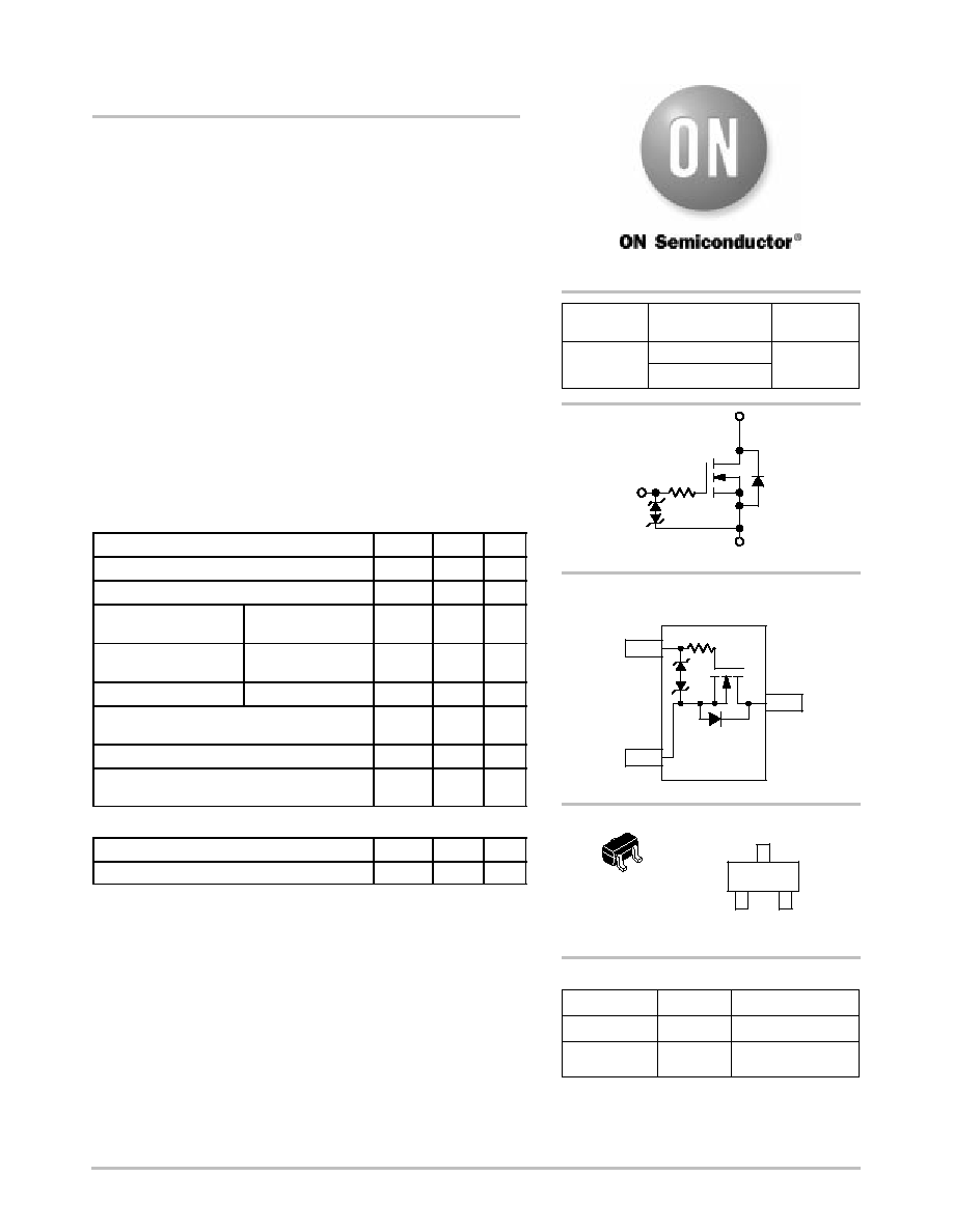
(Top View)
SC-75 / SOT-416
CASE 463
STYLE 5
2
1
SC-75 (3-Leads)
Drain
Gate
3
1
2
Source
3
R
DS(on)
Typ @ V
GS
I
D
MAX
(Note 1)
V
(BR)DSS
7.0
W
@ 4.5 V
30 V
154 mA
1
3
2
N-Channel
MARKING DIAGRAM
T6
= Specific Device Code
M
= Date Code
T6
M
1
3
2
Device
Package
Shipping
ORDERING INFORMATION
NTA7002NT1
SC-75
3000 Tape & Reel
NTA7002NT1G
SC-75
(Pb-Free)
3000 Tape & Reel
PIN CONNECTIONS
For information on tape and reel specifications,
including part orientation and tape sizes, please
refer to our Tape and Reel Packaging Specification
Brochure, BRD8011/D.
http://onsemi.com
NTA7002N
http://onsemi.com
2
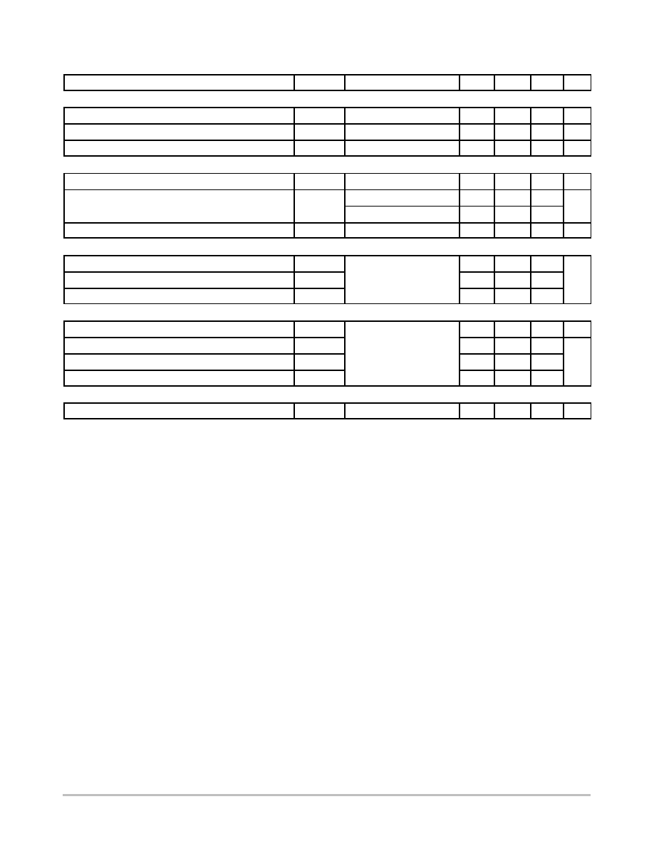
ELECTRICAL CHARACTERISTICS
(T
J
= 25
∞
C unless otherwise specified)
Parameter
Symbol
Test Condition
Min
Typ
Max
Unit
OFF CHARACTERISTICS
Drain-to-Source Breakdown Voltage
V
(BR)DSS
V
GS
= 0 V, I
D
= 100
m
A
30
V
Zero Gate Voltage Drain Current
I
DSS
V
GS
= 0 V, V
DS
= 30 V
1.0
m
A
Gate-to-Source Leakage Current
I
GSS
V
DS
= 0 V, V
GS
=
±
10 V
±
20
m
A
ON CHARACTERISTICS (Note 2)
Gate Threshold Voltage
V
GS(TH)
V
DS
= V
GS
, I
D
= 100
m
A
0.5
1.0
1.5
V
Drain-to-Source On Resistance
R
DS(on)
V
GS
= 4.5 V, I
D
= 154 mA
7.0
W
(
)
V
GS
= 2.5 V, I
D
= 154 mA
7.5
W
Forward Transconductance
g
FS
V
DS
= 3 V, I
D
= 154 mA
80
mS
CAPACITANCES
Input Capacitance
C
ISS
11.5
Output Capacitance
C
OSS
V
DS
= 5.0 V, f = 1 MHz,
V
GS
= 0 V
10
pF
Reverse Transfer Capacitance
C
RSS
V
GS
= 0 V
3.5
SWITCHING CHARACTERISTICS (Note 3)
Turn-On Delay Time
t
d(ON)
13
ns
Rise Time
t
r
V
GS
= 4.5 V, V
DS
= 5.0 V,
15
Turn-Off Delay Time
t
d(OFF)
V
GS
= 4.5 V, V
DS
= 5.0 V,
I
D
= 75 mA, R
G
= 10
W
98
ns
Fall Time
t
f
60
Drain-Source Diode Characteristics
Forward Diode Voltage
V
SD
V
GS
= 0 V, I
S
= 0.154 mA
0.77
0.9
V
2. Pulse Test: pulse width
v
300
m
s, duty cycle
v
2%.
3. Switching characteristics are independent of operating junction temperatures.
NTA7002N
http://onsemi.com
3
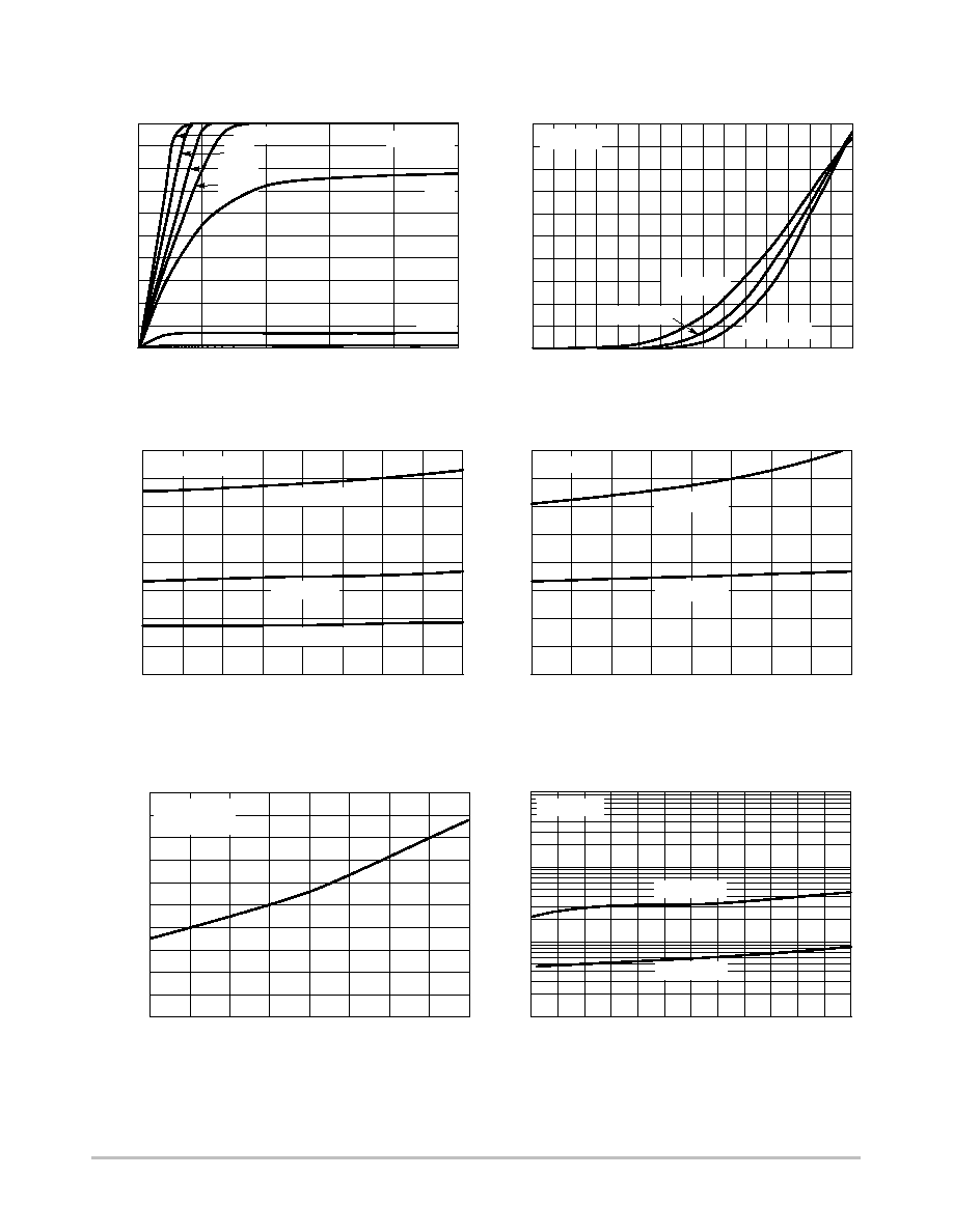
TYPICAL PERFORMANCE CURVES
T
J
= 125
∞
C
0
0.16
1.6
0.4
V
DS
, DRAIN-TO-SOURCE VOLTAGE (VOLTS)
I
D,
DRAIN CURRENT (AMPS)
0.12
0.04
0
Figure 1. On-Region Characteristics
0.6
1.4
2
Figure 2. Transfer Characteristics
V
GS
, GATE-TO-SOURCE VOLTAGE (VOLTS)
1
2
0.5
Figure 3. On-Resistance vs. Drain Current and
Temperature
I
D,
DRAIN CURRENT (AMPS)
R
DS(on),
DRAIN-T
O-SOURCE
RESIST
ANCE (
W
)
I
D,
DRAIN CURRENT (AMPS)
Figure 4. On-Resistance vs. Drain Current and
Gate Voltage
-50
0
-25
25
1
0.2
0
50
150
Figure 5. On-Resistance Variation with
Temperature
T
J
, JUNCTION TEMPERATURE (
∞
C)
T
J
= 25
∞
C
0.05
T
J
= -55
∞
C
T
J
= 125
∞
C
75
T
J
= 25
∞
C
I
D
= 0.15 A
V
GS
= 4.5 V
R
DS(on),
DRAIN-T
O-SOURCE
RESIST
ANCE (NORMALIZED)
T
J
= 25
∞
C
R
DS(on),
DRAIN-T
O-SOURCE
RESIST
ANCE (
W
)
1.2
V
GS
= 2.5 V
0
0.15
1
25
Figure 6. Drain-to-Source Leakage Current
vs. Voltage
V
DS
, DRAIN-TO-SOURCE VOLTAGE (VOLTS)
15
V
GS
= 0 V
I
DSS
, LEAKAGE (nA)
T
J
= 150
∞
C
T
J
= 125
∞
C
V
GS
= 4.5 V
10
100
2 V
V
DS
= 5 V
20
1.4 V
0.08
1.2 V
0.1
30
0.2
0.18
V
GS
= 10 V
2.5
125
100
0
2.0
10
5
1.2
0.8
1.2
1.5
0.2
V
GS
= 4.5 V
T
J
= 25
∞
C
T
J
= -55
∞
C
I
D,
DRAIN CURRENT (AMPS)
2
1000
5 V
2.4 V
1.8
1
1
2
0.5
0.05
0
0.15
0.1
2.5
1.5
0.2
0.4
1.4
0.6
1.6
0.8
1.8
0.14
0.1
0.02
0.06
2.8 V
0.16
0.12
0.04
0
0.08
0.2
0.8
1.6

NTA7002N
http://onsemi.com
4
TYPICAL PERFORMANCE CURVES
Figure 7. Capacitance Variation
0.02
0
V
SD
, SOURCE-TO-DRAIN VOLTAGE (VOLTS)
Figure 8. Resistive Switching Time
Variation vs. Gate Resistance
I
S
, SOURCE CURRENT (AMPS)
V
GS
= 0 V
T
J
= 25
∞
C
0.16
0.5
0.65
Figure 9. Diode Forward Voltage vs. Current
0.8
0.6
0.08
0.06
GATE-TO-SOURCE OR DRAIN-TO-SOURCE VOLTAGE (VOLTS)
C, CAP
ACIT
ANCE (pF)
5
10
0
5
10
5
T
J
= 25
∞
C
C
iss
C
oss
C
rss
15
0
20
C
iss
C
rss
V
DS
= 0 V
V
GS
= 0 V
V
DS
V
GS
R
G
, GATE RESISTANCE (OHMS)
1
10
100
100
10
t, TIME
(ns)
V
DD
= 5.0 V
I
D
= 75 mA
V
GS
= 4.5 V
t
r
t
d(on)
1000
t
f
t
d(off)
1
0.04
25
0.7
0.55
10
15
0.14
20
0.12
0.1
0.75
NTA7002N
http://onsemi.com
5
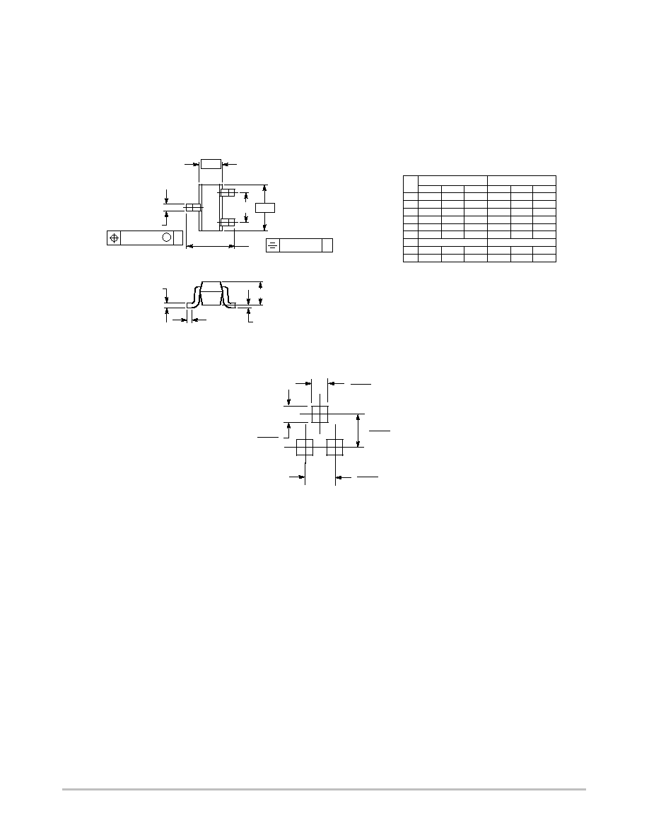
PACKAGE DIMENSIONS
SC-75 / SOT-416
CASE 463-01
ISSUE D
STYLE 5:
PIN 1. GATE
2. SOURCE
3. DRAIN
SOLDERING FOOTPRINT*
1.10
0.043
0.53
0.020
0.50
0.020
0.53
0.020
*For additional information on our Pb-Free strategy and soldering
details, please download the ON Semiconductor Soldering and
Mounting Techniques Reference Manual, SOLDERRM/D.
NOTES:
1. DIMENSIONING AND TOLERANCING PER ANSI
Y14.5M, 1982.
2. CONTROLLING DIMENSION: MILLIMETER.
M
0.20 (0.008)
D
-E-
-D-
b
e
3 PL
0.20 (0.008) E
C
L
A
A1
3
2
1
H
E
DIM
MIN
NOM
MAX
MILLIMETERS
A
0.70
0.80
0.90
A1
0.00
0.05
0.10
b
C
0.10
0.15
0.25
D
1.40
1.60
1.80
E
e
1.00 BSC
0.027
0.031
0.035
0.000
0.002
0.004
0.004
0.006
0.010
0.055
0.062
0.070
0.04 BSC
MIN
NOM
MAX
INCHES
0.15
0.20
0.30
0.006
0.008
0.012
H
E
L
0.10
0.15
0.20
1.45
1.60
1.75
0.004
0.006
0.008
0.057
0.062
0.068
0.70
0.75
0.80
0.027
0.029
0.031
NTA7002N
http://onsemi.com
6
ON Semiconductor and are registered trademarks of Semiconductor Components Industries, LLC (SCILLC). SCILLC reserves the right to make changes without further notice
to any products herein. SCILLC makes no warranty, representation or guarantee regarding the suitability of its products for any particular purpose, nor does SCILLC assume any liability
arising out of the application or use of any product or circuit, and specifically disclaims any and all liability, including without limitation special, consequential or incidental damages.
"Typical" parameters which may be provided in SCILLC data sheets and/or specifications can and do vary in different applications and actual performance may vary over time. All
operating parameters, including "Typicals" must be validated for each customer application by customer's technical experts. SCILLC does not convey any license under its patent rights
nor the rights of others. SCILLC products are not designed, intended, or authorized for use as components in systems intended for surgical implant into the body, or other applications
intended to support or sustain life, or for any other application in which the failure of the SCILLC product could create a situation where personal injury or death may occur. Should
Buyer purchase or use SCILLC products for any such unintended or unauthorized application, Buyer shall indemnify and hold SCILLC and its officers, employees, subsidiaries, affiliates,
and distributors harmless against all claims, costs, damages, and expenses, and reasonable attorney fees arising out of, directly or indirectly, any claim of personal injury or death
associated with such unintended or unauthorized use, even if such claim alleges that SCILLC was negligent regarding the design or manufacture of the part. SCILLC is an Equal
Opportunity/Affirmative Action Employer. This literature is subject to all applicable copyright laws and is not for resale in any manner.
PUBLICATION ORDERING INFORMATION
N. American Technical Support: 800-282-9855 Toll Free
USA/Canada
Japan: ON Semiconductor, Japan Customer Focus Center
2-9-1 Kamimeguro, Meguro-ku, Tokyo, Japan 153-0051
Phone: 81-3-5773-3850
NTA7002N/D
LITERATURE FULFILLMENT:
Literature Distribution Center for ON Semiconductor
P.O. Box 61312, Phoenix, Arizona 85082-1312 USA
Phone: 480-829-7710 or 800-344-3860 Toll Free USA/Canada
Fax: 480-829-7709 or 800-344-3867 Toll Free USA/Canada
Email: orderlit@onsemi.com
ON Semiconductor Website: http://onsemi.com
Order Literature: http://www.onsemi.com/litorder
For additional information, please contact your
local Sales Representative.