⌐
Semiconductor Components Industries, LLC, 2001
January, 2001 ¡ Rev. 0
1
Publication Order Number:
NTD20N03L27/D
NTD20N03L27
Power MOSFET
20 Amps, 30 Volts
N¡Channel DPAK
This logic level vertical power MOSFET is a general purpose part
that provides the "best of design" available today in a low cost power
package. Avalanche energy issues make this part an ideal design in.
The drain¡to¡source diode has a ideal fast but soft recovery.
Features
╖
Ultra¡Low RDS(on), single base, advanced technology
╖
SPICE parameters available
╖
Diode is characterized for use in bridge circuits
╖
IDSS and VDS(on) specified at elevated temperatures
╖
High Avalanche Energy Specified
╖
ESD JEDAC rated HBM Class 1, MM Class A, CDM Class 0
Typical Applications
╖
Power Supplies
╖
Inductive Loads
╖
PWM Motor Controls
╖
Replaces MTD20N03L in many applications
MAXIMUM RATINGS
(TC = 25
░
C unless otherwise noted)
Rating
Symbol
Value
Unit
Drain¡to¡Source Voltage
VDSS
30
Vdc
Drain¡to¡Gate Voltage (RGS = 1.0 M
)
VDGR
30
Vdc
Gate¡to¡Source Voltage
¡ Continuous
¡ Non¡Repetitive (tp
v
10 ms)
VGS
VGS
"
20
"
24
Vdc
Drain Current
¡ Continuous @ TA = 25
_
C
¡ Continuous @ TA = 100
_
C
¡ Single Pulse (tp
v
10
╡
s)
ID
ID
IDM
20
16
60
Adc
Apk
Total Power Dissipation @ TA = 25
_
C
Derate above 25
░
C
Total Power Dissipation @ TC = 25
░
C
(Note 1.)
PD
74
0.6
1.75
Watts
W/
░
C
W
Operating and Storage Temperature
Range
TJ, Tstg
¡55 to
150
░
C
Single Pulse Drain¡to¡Source Avalanche
Energy ¡ Starting TJ = 25
░
C
(VDD = 30 Vdc, VGS = 5 Vdc, L =
1.0 mH, IL(pk) = 24 A, VDS = 34 Vdc)
EAS
288
mJ
Thermal Resistance
¡ Junction¡to¡Case
¡ Junction¡to¡Ambient
¡ Junction¡to¡Ambient (Note 1.)
R
JC
R
JA
R
JA
1.67
100
71.4
░
C/W
Maximum Lead Temperature for Soldering
Purposes, 1/8
from case for 10 seconds
TL
260
░
C
1. When surface mounted to an FR4 board using the minimum recommended
pad size and repetitive rating; pulse width limited by maximum junction
temperature.
20 AMPERES
30 VOLTS
RDS(on) = 27 m
Device
Package
Shipping
ORDERING INFORMATION
NTD20N03L27
DPAK
75 Units/Rail
CASE 369A
DPAK
STYLE 2
PIN ASSIGNMENT
http://onsemi.com
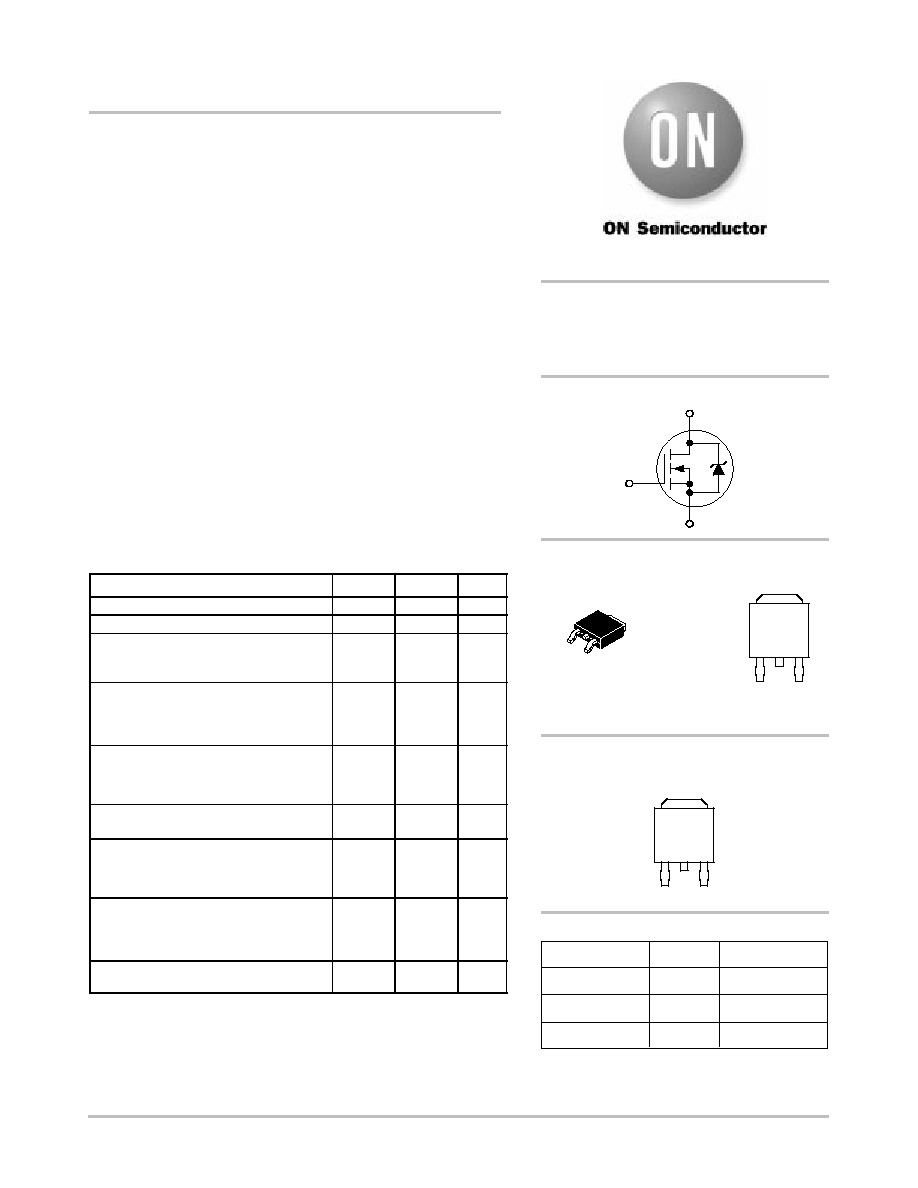
N¡Channel
D
S
G
NTD20N03L27¡1
DPAK
75 Units/Rail
MARKING
DIAGRAM
20N3L
= Device Code
Y
= Year
WW
= Work Week
YWW
20N3L
1
Gate
3
Source
2
Drain
NTD20N03L27T4
DPAK
2500 Tape & Reel
4
Drain
1
2
3
4
NTD20N03L27
http://onsemi.com
2
ELECTRICAL CHARACTERISTICS
(TC = 25
░
C unless otherwise noted)
Characteristic
Symbol
Min
Typ
Max
Unit
OFF CHARACTERISTICS
Drain¡to¡Source Breakdown Voltage (Note 2.)
(VGS = 0 Vdc, ID = 250
╡
Adc)
Temperature Coefficient (Positive)
V(BR)DSS
30
¡
¡
43
¡
¡
Vdc
mV/
░
C
Zero Gate Voltage Drain Current
(VDS = 30 Vdc, VGS = 0 Vdc)
(VDS = 30 Vdc, VGS = 0 Vdc, TJ =150
░
C)
IDSS
¡
¡
¡
¡
10
100
╡
Adc
Gate¡Body Leakage Current (VGS =
▒
20
Vdc, VDS = 0 Vdc)
IGSS
¡
¡
▒
100
nAdc
ON CHARACTERISTICS (Note 2.)
Gate Threshold Voltage (Note 2.)
(VDS = VGS, ID = 250
╡
Adc)
Threshold Temperature Coefficient (Negative)
VGS(th)
1.0
¡
1.6
5.0
2.0
¡
Vdc
mV/
░
C
Static Drain¡to¡Source On¡Resistance (Note 2.)
(VGS = 4.0 Vdc, ID = 10 Adc)
(VGS = 5.0 Vdc, ID = 10 Adc)
RDS(on)
¡
¡
28
23
31
27
m
Static Drain¡to¡Source On¡Resistance (Note 2.)
(VGS = 5.0 Vdc, ID = 20 Adc)
(VGS = 5.0 Vdc, ID = 10 Adc, TJ = 150
░
C)
VDS(on)
¡
¡
0.48
0.40
0.54
¡
Vdc
Forward Transconductance (Note 2.) (VDS = 5.0 Vdc, ID = 10 Adc)
gFS
¡
21
¡
mhos
DYNAMIC CHARACTERISTICS
Input Capacitance
(V
25 Vd
V
0 Vd
Ciss
¡
1005
1260
pF
Output Capacitance
(VDS = 25 Vdc, VGS = 0 Vdc,
f = 1.0 MHz)
Coss
¡
271
420
Transfer Capacitance
f = 1.0 MHz)
Crss
¡
87
112
SWITCHING CHARACTERISTICS (Note 3.)
Turn¡On Delay Time
td(on)
¡
17
25
ns
Rise Time
(VDD = 20 Vdc, ID = 20 Adc,
VGS = 5 0 Vdc
tr
¡
137
160
Turn¡Off Delay Time
VGS = 5.0 Vdc,
RG = 9.1
) (Note 2.)
td(off)
¡
38
45
Fall Time
RG 9.1
) (Note 2.)
tf
¡
31
40
Gate Charge
(V
48 Vd
I
15 Ad
QT
¡
13.8
18.9
nC
(VDS = 48 Vdc, ID = 15 Adc,
VGS = 10 Vdc) (Note 2.)
Q1
¡
2.8
¡
VGS = 10 Vdc) (Note 2.)
Q2
¡
6.6
¡
SOURCE¡DRAIN DIODE CHARACTERISTICS
Forward On¡Voltage
(IS = 20 Adc, VGS = 0 Vdc) (Note 2.)
(IS = 20 Adc, VGS = 0 Vdc, TJ = 125
░
C)
VSD
¡
¡
1.0
0.9
1.15
¡
Vdc
Reverse Recovery Time
trr
¡
23
¡
ns
(IS =15 Adc VGS = 0 Vdc
ta
¡
13
¡
(IS =15 Adc, VGS = 0 Vdc,
dlS/dt = 100 A/
╡
s) (Note 2.)
tb
¡
10
¡
Reverse Recovery Stored
Charge
dlS/dt = 100 A/
╡
s) (Note 2.)
QRR
¡
0.017
¡
╡
C
2. Pulse Test: Pulse Width
300
╡
s, Duty Cycle
2%.
3. Switching characteristics are independent of operating junction temperature.
NTD20N03L27
http://onsemi.com
3
1.6
1.4
1
1.2
0.8
0.6
10
1
100
1000
24
16
28
12
20
0
40
0.015
0
30
1
15
0.4
0.2
¡I
D
, DRAIN CURRENT (AMPS)
0
¡VGS, GATE¡TO¡SOURCE VOLTAGE (V)
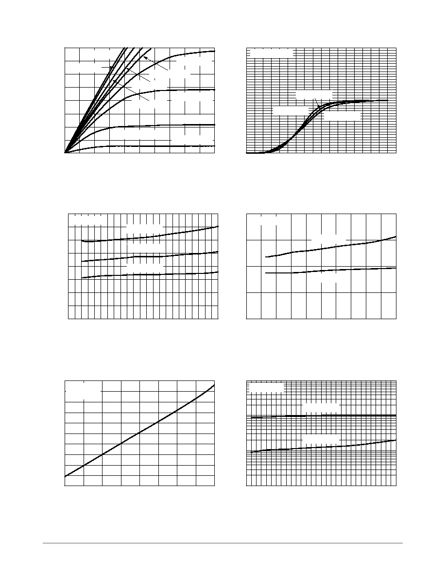
Figure 1. On¡Region Characteristics
Figure 2. Transfer Characteristics
I D
, DRAIN CURRENT (AMPS)
2
0.04
0.035
0.03
0.025
22
15
12
0.02
0.015
0.01
0.005
0
5
25
28
32
Figure 3. On¡Resistance vs. Drain Current and
Temperature
ID, DRAIN CURRENT (AMPS)
Figure 4. On¡Resistance vs. Drain Current and
Gate Voltage
ID, DRAIN CURRENT (AMPS)
Figure 5. On¡Resistance Variation with
Temperature
TJ, JUNCTION TEMPERATURE (
░
C)
Figure 6. Drain¡to¡Source Leakage Current
vs. Voltage
¡VDS, DRAIN¡TO¡SOURCE VOLTAGE (V)
R
DS(on)
, DRAIN¡T
O¡SOURCE RESIST
ANCE (NORMALIZED)
¡I
DSS
, LEAKAGE (nA)
40
¡50
75
50
0
¡25
100
150
0.5
1.5
5
0
28
32
24
20
36
16
40
0.02
0.01
0.025
0.03
0
12
15
9
6
18
3
30
¡VDS, DRAIN¡TO¡SOURCE VOLTAGE (V)
5
10
20
25
35
1.4
2
4
0.6
0.8
1.2
1.6
1.8
1
2
2.5
3
3.5
4
4.5
8
18
35
38
R
DS(on)
, DRAIN¡T
O¡SOURCE RESIST
ANCE (
)
R
DS(on)
, DRAIN¡T
O¡SOURCE RESIST
ANCE (
)
4
8
12
125
25
21
24
27
VGS = 10 V
VGS = 8 V
VGS = 6 V
VGS = 5 V
VGS = 4.5 V
VGS = 4 V
VGS = 3.5 V
VGS = 3 V
VGS = 2.5 V
8
32
36
TJ = 25
░
C
TJ = 100
░
C
TJ = ¡55
░
C
VDS > = 10 V
VGS = 5 V
TJ = 25
░
C
TJ = 100
░
C
TJ = ¡55
░
C
VGS = 5 V
VGS = 10 V
TJ = 25
░
C
ID = 10 A
VGS = 5 V
TJ = 100
░
C
TJ = 125
░
C
VGS = 0 V
TJ = 25
░
C
NTD20N03L27
http://onsemi.com
4
4
350
300
200
250
150
100
0
8
4
10
2
6
0
12
14
10
1500
8
2
4
C, CAP
ACIT
ANCE (pF)
0
Qg, TOTAL GATE CHARGE (nC)
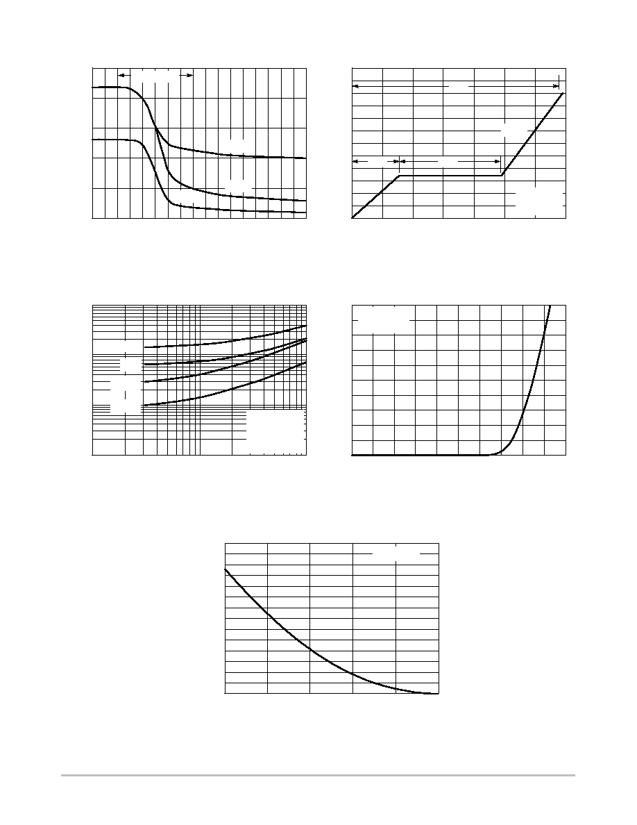
Figure 7. Capacitance Variation
Figure 8. Gate¡to¡Source and
Drain¡to¡Source Voltage vs. Total Charge
V
GS
, GA
TE¡T
O¡SOURCE VOL
T
AGE (V)
1
1000
100
10
10
1
100
Figure 9. Resistive Switching Time Variation
vs. Gate Resistance
RG, GATE RESISTANCE (
)
Figure 10. Diode Forward Voltage vs. Current
VSD, SOURCE¡TO¡DRAIN VOLTAGE (V)
I S
, SOURCE CURRENT (AMPS)
t, TIME (ns)
Figure 11. Maximum Avalanche Energy vs.
Starting Junction Temperature
TJ, STARTING JUNCTION TEMPERATURE (
░
C)
E
AS
, SINGLE PULSE DRAIN¡T
O¡SOURCE
A
V
ALANCHE ENERGY (mJ)
2500
25
125
100
75
50
150
0
6
14
0.0
0.4
0.5
0.3
0.2
0.6
0.1
1.0
10
16
8
12
0
18
20
GATE¡TO¡SOURCE OR DRAIN¡TO¡SOURCE VOLTAGE (V)
500
1000
200
14
25
8
6
2
0
6
10 12
16 18 20 23
2
4
8
10
12
6
4
2
0.7
0.8
0.9
50
VGS ¡ VDS
Ciss
Coss
Crss
Q1
Q2
Q
ID = 20 A
TJ = 25
░
C
VGS
VDS = 20 V
ID = 20 A
VGS = 5.0 V
TJ = 25
░
C
tr
tf
td(off)
td(on)
VGS = 0 V
TJ = 25
░
C
ID = 24 A
NTD20N03L27
http://onsemi.com
5
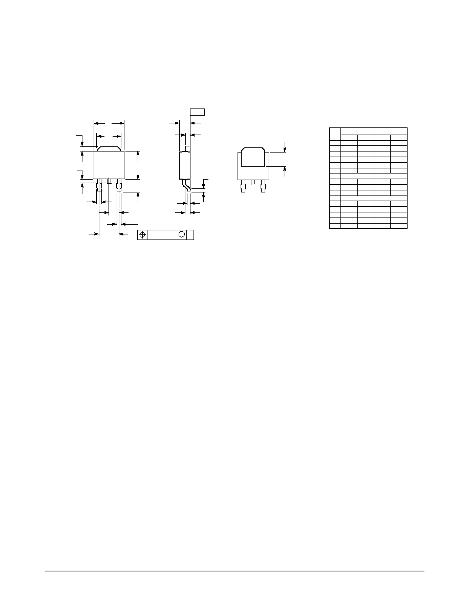
PACKAGE DIMENSIONS
STYLE 2:
PIN 1. GATE
2. DRAIN
3. SOURCE
4. DRAIN
D
A
K
B
R
V
S
F
L
G
2 PL
M
0.13 (0.005)
T
E
C
U
J
H
¡T¡
SEATING
PLANE
Z
DIM
MIN
MAX
MIN
MAX
MILLIMETERS
INCHES
A
0.235
0.250
5.97
6.35
B
0.250
0.265
6.35
6.73
C
0.086
0.094
2.19
2.38
D
0.027
0.035
0.69
0.88
E
0.033
0.040
0.84
1.01
F
0.037
0.047
0.94
1.19
G
0.180 BSC
4.58 BSC
H
0.034
0.040
0.87
1.01
J
0.018
0.023
0.46
0.58
K
0.102
0.114
2.60
2.89
L
0.090 BSC
2.29 BSC
R
0.175
0.215
4.45
5.46
S
0.020
0.050
0.51
1.27
U
0.020
---
0.51
---
V
0.030
0.050
0.77
1.27
Z
0.138
---
3.51
---
NOTES:
1. DIMENSIONING AND TOLERANCING PER ANSI
Y14.5M, 1982.
2. CONTROLLING DIMENSION: INCH.
1
2
3
4
DPAK
CASE 369A¡13
ISSUE AA

NTD20N03L27
http://onsemi.com
6
Notes

NTD20N03L27
http://onsemi.com
7
Notes

NTD20N03L27
http://onsemi.com
8
ON Semiconductor and are trademarks of Semiconductor Components Industries, LLC (SCILLC). SCILLC reserves the right to make changes
without further notice to any products herein. SCILLC makes no warranty, representation or guarantee regarding the suitability of its products for any particular
purpose, nor does SCILLC assume any liability arising out of the application or use of any product or circuit, and specifically disclaims any and all liability,
including without limitation special, consequential or incidental damages. "Typical" parameters which may be provided in SCILLC data sheets and/or
specifications can and do vary in different applications and actual performance may vary over time. All operating parameters, including "Typicals" must be
validated for each customer application by customer's technical experts. SCILLC does not convey any license under its patent rights nor the rights of others.
SCILLC products are not designed, intended, or authorized for use as components in systems intended for surgical implant into the body, or other applications
intended to support or sustain life, or for any other application in which the failure of the SCILLC product could create a situation where personal injury or
death may occur. Should Buyer purchase or use SCILLC products for any such unintended or unauthorized application, Buyer shall indemnify and hold
SCILLC and its officers, employees, subsidiaries, affiliates, and distributors harmless against all claims, costs, damages, and expenses, and reasonable
attorney fees arising out of, directly or indirectly, any claim of personal injury or death associated with such unintended or unauthorized use, even if such claim
alleges that SCILLC was negligent regarding the design or manufacture of the part. SCILLC is an Equal Opportunity/Affirmative Action Employer.
PUBLICATION ORDERING INFORMATION
CENTRAL/SOUTH AMERICA:
Spanish Phone: 303¡308¡7143 (Mon¡Fri 8:00am to 5:00pm MST)
Email: ONlit¡spanish@hibbertco.com
Toll¡Free from Mexico: Dial 01¡800¡288¡2872 for Access ¡
then Dial 866¡297¡9322
ASIA/PACIFIC: LDC for ON Semiconductor ¡ Asia Support
Phone: 303¡675¡2121 (Tue¡Fri 9:00am to 1:00pm, Hong Kong Time)
Toll Free from Hong Kong & Singapore:
001¡800¡4422¡3781
Email: ONlit¡asia@hibbertco.com
JAPAN: ON Semiconductor, Japan Customer Focus Center
4¡32¡1 Nishi¡Gotanda, Shinagawa¡ku, Tokyo, Japan 141¡0031
Phone: 81¡3¡5740¡2700
Email: r14525@onsemi.com
ON Semiconductor Website: http://onsemi.com
For additional information, please contact your local
Sales Representative.
NTD20N03L27/D
NORTH AMERICA Literature Fulfillment:
Literature Distribution Center for ON Semiconductor
P.O. Box 5163, Denver, Colorado 80217 USA
Phone: 303¡675¡2175 or 800¡344¡3860 Toll Free USA/Canada
Fax: 303¡675¡2176 or 800¡344¡3867 Toll Free USA/Canada
Email: ONlit@hibbertco.com
Fax Response Line: 303¡675¡2167 or 800¡344¡3810 Toll Free USA/Canada
N. American Technical Support: 800¡282¡9855 Toll Free USA/Canada
EUROPE: LDC for ON Semiconductor ¡ European Support
German Phone: (+1) 303¡308¡7140 (Mon¡Fri 2:30pm to 7:00pm CET)
Email: ONlit¡german@hibbertco.com
French Phone: (+1) 303¡308¡7141 (Mon¡Fri 2:00pm to 7:00pm CET)
Email: ONlit¡french@hibbertco.com
English Phone: (+1) 303¡308¡7142 (Mon¡Fri 12:00pm to 5:00pm GMT)
Email: ONlit@hibbertco.com
EUROPEAN TOLL¡FREE ACCESS*: 00¡800¡4422¡3781
*Available from Germany, France, Italy, UK, Ireland