©
Semiconductor Components Industries, LLC, 2004
October, 2004 - Rev. 7
1
Publication Order Number:
NTD2955/D
NTD2955
Power MOSFET
-60 V, -12 A, P-Channel DPAK
This Power MOSFET is designed to withstand high energy in the
avalanche and commutation modes. Designed for low-voltage, high-
speed switching applications in power supplies, converters, and power
motor controls, these devices are particularly well suited for bridge
circuits where diode speed and commutating safe operating areas are
critical and offer an additional safety margin against unexpected
voltage transients.
Features
∑
Avalanche Energy Specified
∑
I
DSS
and V
DS(on)
Specified at Elevated Temperature
∑
Designed for Low-Voltage, High-Speed Switching Applications and
to Withstand High Energy in the Avalanche and Commutation Modes
∑
Pb-Free Packages are Available
MAXIMUM RATINGS
(T
J
= 25
∞
C unless otherwise noted)
Rating
Symbol
Value
Unit
Drain-to-Source Voltage
V
DSS
-60
Vdc
Gate-to-Source Voltage
- Continuous
- Non-repetitive (t
p
10 ms)
V
GS
V
GSM
±
20
±
25
Vdc
Vpk
Drain Current
Drain Current
- Continuous @ T
a
= 25
∞
C
Drain Current
- Single Pulse (t
p
10 ms)
I
D
I
DM
-12
-36
Adc
Apk
Total Power Dissipation @ T
a
= 25
∞
C
P
D
55
W
Operating and Storage Temperature
Range
T
J
, T
stg
- 55 to
175
∞
C
Single Pulse Drain-to-Source Avalanche
Energy - Starting T
J
= 25
∞
C
(V
DD
= 25 Vdc, V
GS
= 10 Vdc, Peak
I
L
= 12 Apk, L = 3.0 mH, R
G
= 25
W
)
E
AS
216
mJ
Thermal Resistance
- Junction-to-Case
- Junction-to-Ambient (Note 1)
- Junction-to-Ambient (Note 2)
R
q
JC
R
q
JA
R
q
JA
2.73
71.4
100
∞
C/W
Maximum Lead Temperature for Soldering
Purposes, 1/8 in. from case for
10 seconds
T
L
260
∞
C
Maximum ratings are those values beyond which device damage can occur.
Maximum ratings applied to the device are individual stress limit values (not
normal operating conditions) and are not valid simultaneously. If these limits
are exceeded, device functional operation is not implied, damage may occur
and reliability may be affected.
1. When surface mounted to an FR4 board using 1 in pad size
(Cu area = 1.127 in
2
).
2. When surface mounted to an FR4 board using the minimum recommended
pad size (Cu area = 0.412 in
2
).
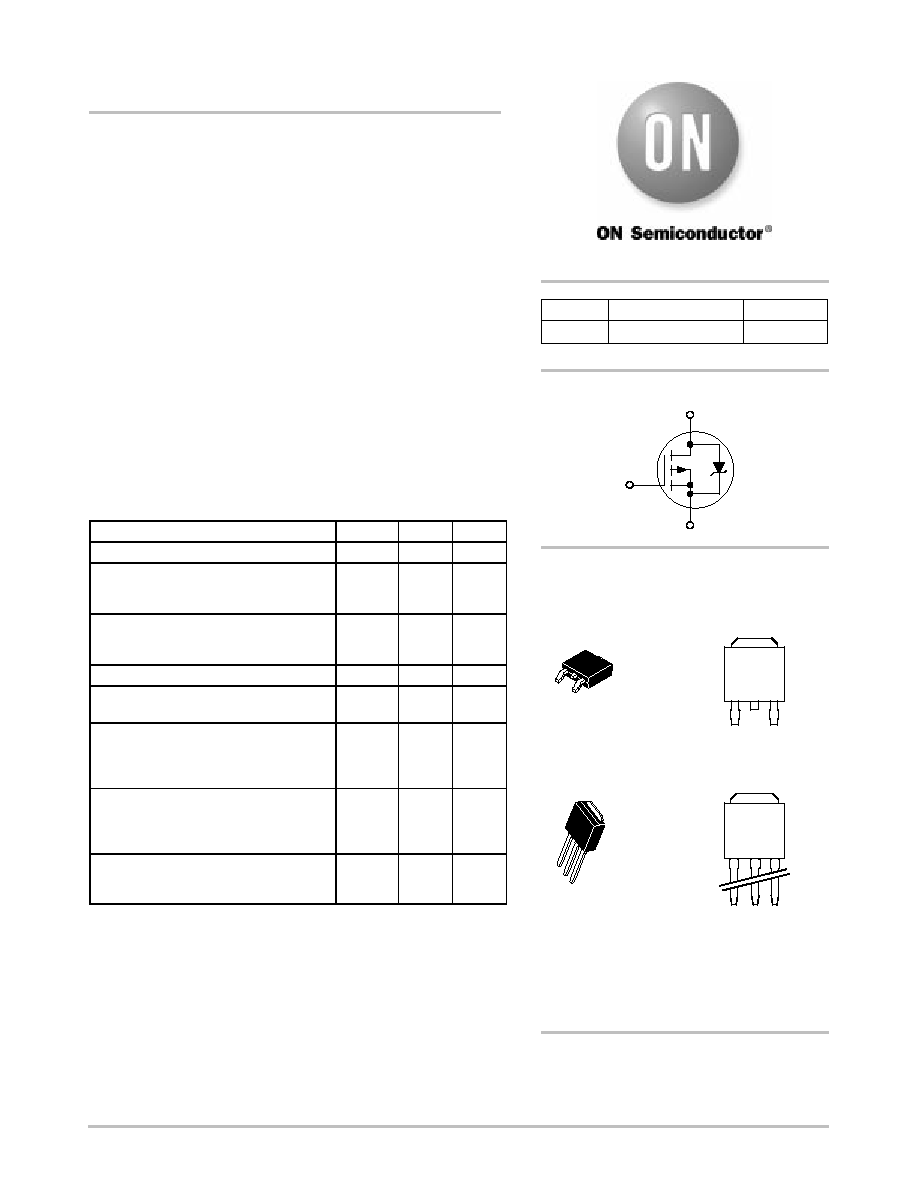
D
S
G
P-Channel
http://onsemi.com
-60 V
155 m
W
@ -10 V, 6 A
R
DS(on)
TYP
-12 A
I
D
MAX
V
(BR)DSS
NT2955
Device Code
A
= Assembly Location
Y
= Year
W
= Work Week
1
Gate
3
Source
2
Drain
4
Drain
DPAK
CASE 369C
STYLE 2
MARKING
DIAGRAMS
1 2
3
4
1
Gate
3
Source
2
Drain
4
Drain
DPAK-3
CASE 369D
STYLE 2
1
2
3
4
AY
W
NT2955
AY
W
NT2955
See detailed ordering and shipping information in the package
dimensions section on page 6 of this data sheet.
ORDERING INFORMATION

NTD2955
http://onsemi.com
2
ELECTRICAL CHARACTERISTICS
(T
J
= 25
∞
C unless otherwise noted)
Characteristic
Symbol
Min
Typ
Max
Unit
OFF CHARACTERISTICS
Drain-to-Source Breakdown Voltage (Note 3)
(V
GS
= 0 Vdc, I
D
= -0.25 mA)
(Positive Temperature Coefficient)
V
(BR)DSS
-60
-
-
67
-
-
Vdc
mV/
∞
C
Zero Gate Voltage Drain Current
(V
GS
= 0 Vdc, V
DS
= -60 Vdc, T
J
= 25
∞
C)
(V
GS
= 0 Vdc, V
DS
= -60 Vdc, T
J
= 150
∞
C)
I
DSS
-
-
-
-
-10
-100
m
Adc
Gate-Body Leakage Current (V
GS
=
±
20 Vdc, V
DS
= 0 Vdc)
I
GSS
-
-
-100
nAdc
ON CHARACTERISTICS (Note 3)
Gate Threshold Voltage
(V
DS
= V
GS
, I
D
= -250
m
Adc)
(Negative Temperature Coefficient)
V
GS(th)
-2.0
-
-2.8
4.5
-4.0
-
Vdc
mV/
∞
C
Static Drain-Source On-State Resistance
(V
GS
= -10 Vdc, I
D
= -6.0 Adc)
R
DS(on)
-
0.155
0.180
W
Drain-to-Source On-Voltage
(V
GS
= -10 Vdc, I
D
= -12 Adc)
(V
GS
= -10 Vdc, I
D
= -6.0 Adc, T
J
= 150
∞
C)
V
DS(on)
-1.86
-
-2.6
-2.0
Vdc
Forward Transconductance (V
DS
= 10 Vdc, I
D
= 6.0 Adc)
gFS
8.0
-
Mhos
DYNAMIC CHARACTERISTICS
Input Capacitance
C
iss
-
500
750
pF
Output Capacitance
(V
DS
= -25 Vdc, V
GS
= 0 Vdc,
F = 1.0 MHz)
C
oss
-
150
250
Reverse Transfer Capacitance
F = 1.0 MHz)
C
rss
-
50
100
SWITCHING CHARACTERISTICS (Notes 3 and 4)
Turn-On Delay Time
t
d(on)
-
10
20
ns
Rise Time
(V
DD
= -30 Vdc, I
D
= -12 A,
t
r
-
45
85
Turn-Off Delay Time
(V
DD
= -30 Vdc, I
D
= -12 A,
V
GS
= -10 V, R
G
= 9.1
W
)
t
d(off)
-
26
40
Fall Time
t
f
-
48
90
Gate Charge
Q
T
-
15
30
nC
(V
DS
= -48 Vdc, V
GS
= -10 Vdc,
I
D
= -12 A)
Q
GS
-
4.0
-
I
D
= -12 A)
Q
GD
-
7.0
-
DRAIN-SOURCE DIODE CHARACTERISTICS (Note 3)
Diode Forward On-Voltage
(I
S
= 12 Adc, V
GS
= 0 V)
(I
S
= 12 Adc, V
GS
= 0 V, T
J
= 150
∞
C)
V
SD
-
-
-1.6
-1.3
-2.5
-
Vdc
Reverse Recovery Time
(I
12 A dI /dt
100 A/
V
0 V)
t
rr
-
50
ns
(I
S
= 12 A, dI
S
/dt = 100 A/
m
s ,V
GS
= 0 V)
t
a
-
40
-
t
b
-
10
-
Reverse Recovery Stored Charge
Q
RR
-
0.10
-
m
C
3. Indicates Pulse Test: Pulse Width
300
m
s, Duty Cycle
2%.
4. Switching characteristics are independent of operating junction temperature.

NTD2955
http://onsemi.com
3
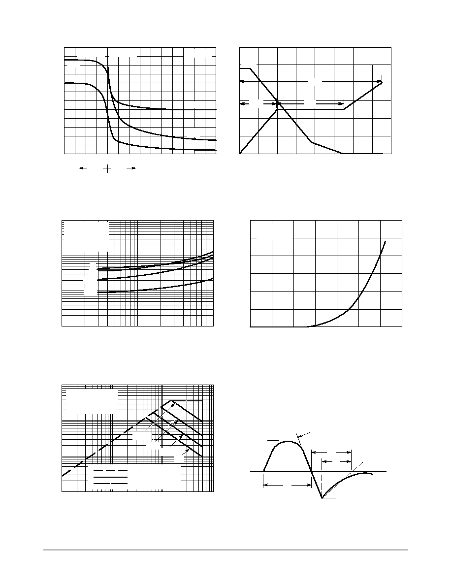
TYPICAL PERFORMANCE CURVES
(T
J
= 25
∞
C unless otherwise noted)
Figure 1. On-Region Characteristics
Figure 2. Transfer Characteristics
Figure 3. On-Resistance versus Drain Current
and Temperature
Figure 4. On-Resistance versus Drain Current
and Gate Voltage
Figure 5. On-Resistance Variation with
Temperature
Figure 6. Drain-To-Source Leakage
Current versus Voltage
0
1
2
3
4
5
0
15
25
-V
DS
, DRAIN-TO-SOURCE VOLTAGE (VOLTS)
2
4
6
8
10
0
10
18
24
-V
GS
, GATE-TO-SOURCE VOLTAGE (VOLTS)
T
J
= 25
∞
C
V
DS
-10 V
T
J
= - 55
∞
C
25
∞
C
125
∞
C
V
GS
= -10 V
-9 V
-8 V
-6 V
-5 V
-7 V
5
10
20
3
5
7
9
4
12
22
6
7
8
9
10
16
6
0
3
6
15
24
0
0.10
0.20
0.30
0
6
21
24
0.050
0.075
0.200
0.250
-I
D
, DRAIN CURRENT (AMPS)
-
I
D
, DRAIN CURRENT (AMPS)
T
J
= 25
∞
C
V
GS
= -10 V
T
J
= 125
∞
C
25
∞
C
- 55
∞
C
12
21
3
12
15
0.05
0.15
0.25
0.100
0.225
0.125
V
GS
= -10 V
-
15 V
18
9
0.35
0.40
0.175
9
18
0.150
- 50
0.6
0.8
1.2
1.6
5
20
50
60
1
100
1000
T
J
, JUNCTION TEMPERATURE (
∞
C)
-V
DS
, DRAIN-TO-SOURCE VOLTAGE (VOLTS)
- 25
0
25
50
75
100
125
150
V
GS
= 0 V
V
GS
= -10 V
I
D
= -6 A
15
30
40
1.0
1.4
T
J
= 125
∞
C
175
0.4
0.2
0
1.8
2.0
100
∞
C
-6.5 V
-5.5 V
-9.5 V
8
2
20
14
0.45
0.50
10
10
25
55
35
45
-I
D,
DRAIN CURRENT (A)
-I
D,
DRAIN CURRENT (A)
R
DS(on),
DRAIN-T
O-SOURCE RESIST
ANCE (
)
R
DS(on),
DRAIN-T
O-SOURCE RESIST
ANCE (
)
R
DS(on),
DRAIN-T
O-SOURCE RESIST
ANCE (NORMALIZED)
-I
DSS
, LEAKAGE (nA)
NTD2955
http://onsemi.com
4
0.1
1
10
100
0.1
1
10
100
Figure 7. Capacitance Variation
Figure 8. Gate-To-Source and Drain-To-Source
Voltage versus Total Charge
Figure 9. Resistive Switching Time
Variation versus Gate Resistance
R
G
, GATE RESISTANCE (
W
)
1
10
100
t, TIME
(ns)
V
DD
= -30 V
I
D
= -12 A
V
GS
= -10 V
T
J
= 25
∞
C
t
f
t
d(off)
0
Q
T
, TOTAL GATE CHARGE (nC)
2
4
6
8
I
D
= 12 A
T
J
= 25
∞
C
V
GS
1000
100
10
1
15
10
0
2.5
5
60
50
40
30
0
V
DS
14
Q
T
Q
GS
Q
GD
16
10
12
t
d(on)
t
r
12.5
7.5
20
0
0.25
0.75
1.75
-V
SD
, SOURCE-TO-DRAIN VOLTAGE (V)
V
GS
= 0 V
T
J
= 25
∞
C
0
10
15
5
0.5
1
1.25
1.5
10
10
0
10
15
25
GATE-TO-SOURCE OR DRAIN-TO-SOURCE VOLTAGE (V)
C, CAP
ACIT
ANCE (pF)
-V
GS
-V
DS
T
J
= 25
∞
C
V
DS
= 0 V
V
GS
= 0 V
1000
800
600
400
200
0
20
C
iss
C
oss
C
rss
5
5
C
iss
C
rss
1200
Figure 10. Diode Forward Voltage versus Current
Figure 11. Maximum Rated Forward Biased
Safe Operating Area
-V
DS
, DRAIN-TO-SOURCE VOLTAGE (V)
V
GS
= -15 V
SINGLE PULSE
T
C
= 25
∞
C
dc
100 ms
1 ms
10 ms
R
DS(on)
LIMIT
THERMAL LIMIT
PACKAGE LIMIT
Figure 12. Diode Reverse Recovery Waveform
di/dt
t
rr
t
a
t
p
I
S
0.25 I
S
TIME
I
S
t
b
-V
DS
, DRAIN-T
O-SOURCE VOL
T
AGE (V)
-V
GS
, GA
TE-T
O-SOURCE VOL
T
AGE (V)
-I
S
, SOURCE CURRENT (AMPS)
-V
DS
, DRAIN-T
O-SOURCE VOL
T
AGE (V)
NTD2955
http://onsemi.com
5
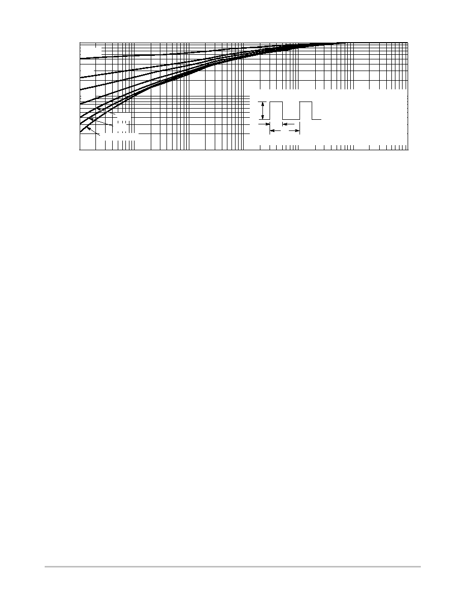
Figure 13. Thermal Response
t, TIME (s)
r(t)
, NORMALIZED EFFECTIVE
TRANSIENT
THERMAL
RESIST
ANCE
R
qJC
(t) = r(t) R
qJC
D CURVES APPLY FOR POWER
PULSE TRAIN SHOWN
READ TIME AT t
1
T
J(pk)
- T
C
= P
(pk)
R
qJC
(t)
P
(pk)
t
1
t
2
DUTY CYCLE, D = t
1
/t
2
1.0
0.1
0.01
0.2
D = 0.5
0.05
0.01
SINGLE PULSE
0.1
1.0E-05
1.0E-04
1.0E-03
1.0E-02
1.0E-01
1.0E+00
1.0E+01
0.02