©
Semiconductor Components Industries, LLC, 2004
August, 2004 - Rev. 4
1
Publication Order Number:
NTD3055L104/D
NTD3055L104
Power MOSFET
12 Amps, 60 Volts, Logic Level
N-Channel DPAK
Designed for low voltage, high speed switching applications in
power supplies, converters and power motor controls and bridge
circuits.
Features
∑
Pb-Free Packages are Available
∑
Lower R
DS(on)
∑
Lower V
DS(on)
∑
Tighter V
SD
Specification
∑
Lower Diode Reverse Recovery Time
∑
Lower Reverse Recovery Stored Charge
Typical Applications
∑
Power Supplies
∑
Converters
∑
Power Motor Controls
∑
Bridge Circuits
MAXIMUM RATINGS
(T
J
= 25
∞
C unless otherwise noted)
Rating
Symbol
Value
Unit
Drain-to-Source Voltage
V
DSS
60
Vdc
Drain-to-Gate Voltage (R
GS
= 10 M
W
)
V
DGR
60
Vdc
Gate-to-Source Voltage, Continuous
- Non-Repetitive (t
p
v
10 ms)
V
GS
V
GS
"
15
"
20
Vdc
Drain Current
- Continuous @ T
A
= 25
∞
C
- Continuous @ T
A
= 100
∞
C
- Single Pulse (t
p
v
10
m
s)
I
D
I
D
I
DM
12
10
45
Adc
Apk
Total Power Dissipation @ T
A
= 25
∞
C
Derate above 25
∞
C
Total Power Dissipation @ T
A
= 25
∞
C (Note 1)
Total Power Dissipation @ T
A
= 25
∞
C (Note 2)
P
D
48
0.32
2.1
1.5
W
W/
∞
C
W
W
Operating and Storage Temperature Range
T
J
, T
stg
- 55 to
+175
∞
C
Single Pulse Drain-to-Source Avalanche
Energy - Starting T
J
= 25
∞
C
(V
DD
= 25 Vdc, V
GS
= 5.0 Vdc, L = 1.0 mH
I
L(pk)
= 11 A, V
DS
= 60 Vdc)
E
AS
61
mJ
Thermal Resistance, - Junction-to-Case
- Junction-to-Ambient (Note 1)
- Junction-to-Ambient (Note 2)
R
q
JC
R
q
JA
R
q
JA
3.13
71.4
100
∞
C/W
Maximum Lead Temperature for Soldering
Purposes, 1/8
from case for 10 seconds
T
L
260
∞
C
Maximum ratings are those values beyond which device damage can occur.
Maximum ratings applied to the device are individual stress limit values (not
normal operating conditions) and are not valid simultaneously. If these limits
are exceeded, device functional operation is not implied, damage may occur
and reliability may be affected.
1. When surface mounted to an FR4 board using 1
pad size,
(Cu Area 1.127 in
2
).
2. When surface mounted to an FR4 board using the minimum recommended
pad size, (Cu Area 0.412 in
2
).
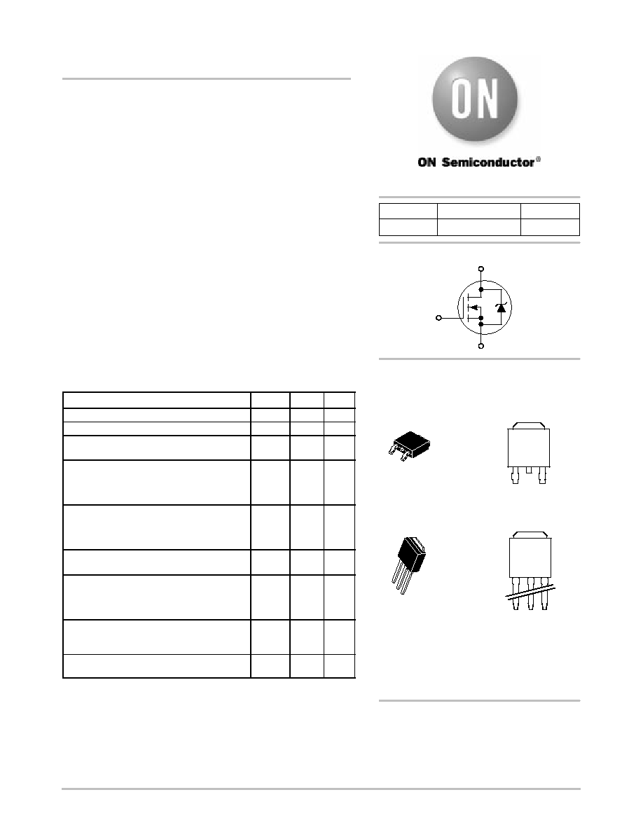
N-Channel
D
S
G
60 V
104 m
W
R
DS(on)
TYP
12 A
I
D
MAX
V
(BR)DSS
See detailed ordering and shipping information in the package
dimensions section on page 2 of this data sheet.
ORDERING INFORMATION
1
Gate
3
Source
2
Drain
4
Drain
DPAK
CASE 369C
STYLE 2
MARKING
DIAGRAMS
1 2
3
4
1
Gate
3
Source
2
Drain
4
Drain
DPAK-3
CASE 369D
STYLE 2
1
2
3
4
AY
W
55L104
AY
W
55L104
55L104
= Device Code
A
= Assembly Location
Y
= Year
W
= Work Week
http://onsemi.com
NTD3055L104
http://onsemi.com
2
ELECTRICAL CHARACTERISTICS
(T
J
= 25
∞
C unless otherwise noted)
Characteristic
Symbol
Min
Typ
Max
Unit
OFF CHARACTERISTICS
Drain-to-Source Breakdown Voltage (Note 3)
(V
GS
= 0 Vdc, I
D
= 250
m
Adc)
Temperature Coefficient (Positive)
V
(BR)DSS
60
-
70
62.9
-
-
Vdc
mV/
∞
C
Zero Gate Voltage Drain Current
(V
DS
= 60 Vdc, V
GS
= 0 Vdc)
(V
DS
= 60 Vdc, V
GS
= 0 Vdc, T
J
= 150
∞
C)
I
DSS
-
-
-
-
1.0
10
m
Adc
Gate-Body Leakage Current (V
GS
=
±
15
Vdc, V
DS
= 0 Vdc)
I
GSS
-
-
±
100
nAdc
ON CHARACTERISTICS (Note 3)
Gate Threshold Voltage (Note 3)
(V
DS
= V
GS
, I
D
= 250
m
Adc)
Threshold Temperature Coefficient (Negative)
V
GS(th)
1.0
-
1.6
4.2
2.0
-
Vdc
mV/
∞
C
Static Drain-to-Source On-Resistance (Note 3)
(V
GS
= 5.0 Vdc, I
D
= 6.0 Adc)
R
DS(on)
-
89
104
m
W
Static Drain-to-Source On-Voltage (Note 3)
(V
GS
= 5.0 Vdc, I
D
= 12 Adc)
(V
GS
= 5.0 Vdc, I
D
= 6.0 Adc, T
J
= 150
∞
C)
V
DS(on)
-
-
0.98
0.86
1.50
-
Vdc
Forward Transconductance (Note 3) (V
DS
= 8.0 Vdc, I
D
= 6.0 Adc)
g
FS
-
9.1
-
mhos
DYNAMIC CHARACTERISTICS
Input Capacitance
(V
25 Vdc V
0 Vdc
C
iss
-
316
440
pF
Output Capacitance
(V
DS
= 25 Vdc, V
GS
= 0 Vdc,
f = 1.0 MHz)
C
oss
-
105
150
Transfer Capacitance
f = 1.0 MHz)
C
rss
-
35
70
SWITCHING CHARACTERISTICS (Note 4)
Turn-On Delay Time
t
d(on)
-
9.2
20
ns
Rise Time
(V
DD
= 30 Vdc, I
D
= 12 Adc,
t
r
-
104
210
Turn-Off Delay Time
(V
DD
30 Vdc, I
D
12 Adc,
V
GS
= 5.0 Vdc, R
G
= 9.1
W
) (Note 3)
t
d(off)
-
19
40
Fall Time
GS
G
t
f
-
40.5
80
Gate Charge
(V
48 Vdc I
12 Adc
Q
T
-
7.4
20
nC
Ga e C a ge
(V
DS
= 48 Vdc, I
D
= 12 Adc,
V
GS
= 5 0 Vdc) (Note 3)
Q
1
-
2.0
-
V
GS
= 5.0 Vdc) (Note 3)
Q
2
-
4.0
-
SOURCE-DRAIN DIODE CHARACTERISTICS
Forward On-Voltage
(I
S
= 12 Adc, V
GS
= 0 Vdc) (Note 3)
(I
S
= 12 Adc, V
GS
= 0 Vdc, T
J
= 150
∞
C)
V
SD
-
-
0.95
0.82
1.2
-
Vdc
Reverse Recovery Time
(I
12 Adc V
0 Vdc
t
rr
-
35
-
ns
e e se
eco e y
e
(I
S
= 12 Adc, V
GS
= 0 Vdc,
dI
S
/dt = 100 A/
m
s) (Note 3)
t
a
-
21
-
s
dI
S
/dt = 100 A/
m
s) (Note 3)
t
b
-
14
-
Reverse Recovery Stored Charge
Q
RR
-
0.04
-
m
C
3. Pulse Test: Pulse Width
300
m
s, Duty Cycle
2%.
4. Switching characteristics are independent of operating junction temperatures.
ORDERING INFORMATION
Device
Package
Shipping
NTD3055L104
DPAK
75 Units/Rail
NTD3055L104G
DPAK
(Pb-Free)
75 Units/Rail
NTD3055L104-1
DPAK-3
75 Units/Rail
NTD3055L104-1G
DPAK-3
(Pb-Free)
75 Units/Rail
NTD3055L104T4
DPAK
2500 Tape & Reel
NTD3055L104T4G
DPAK
(Pb-Free)
2500 Tape & Reel
For information on tape and reel specifications, including part orientation and tape sizes, please refer to our Tape and Reel Packaging
Specifications Brochure, BRD8011/D.
NTD3055L104
http://onsemi.com
3
0
0.12
16
12
0.08
0.04
0
8
20
0.32
24
1.6
1.2
1.4
1
0.8
0.6
1
100
10,000
0
8
8
2
1
V
DS
, DRAIN-TO-SOURCE VOLTAGE (VOLTS)
I
D
, DRAIN CURRENT (AMPS)
0
V
GS
, GATE-TO-SOURCE VOLTAGE (VOLTS)
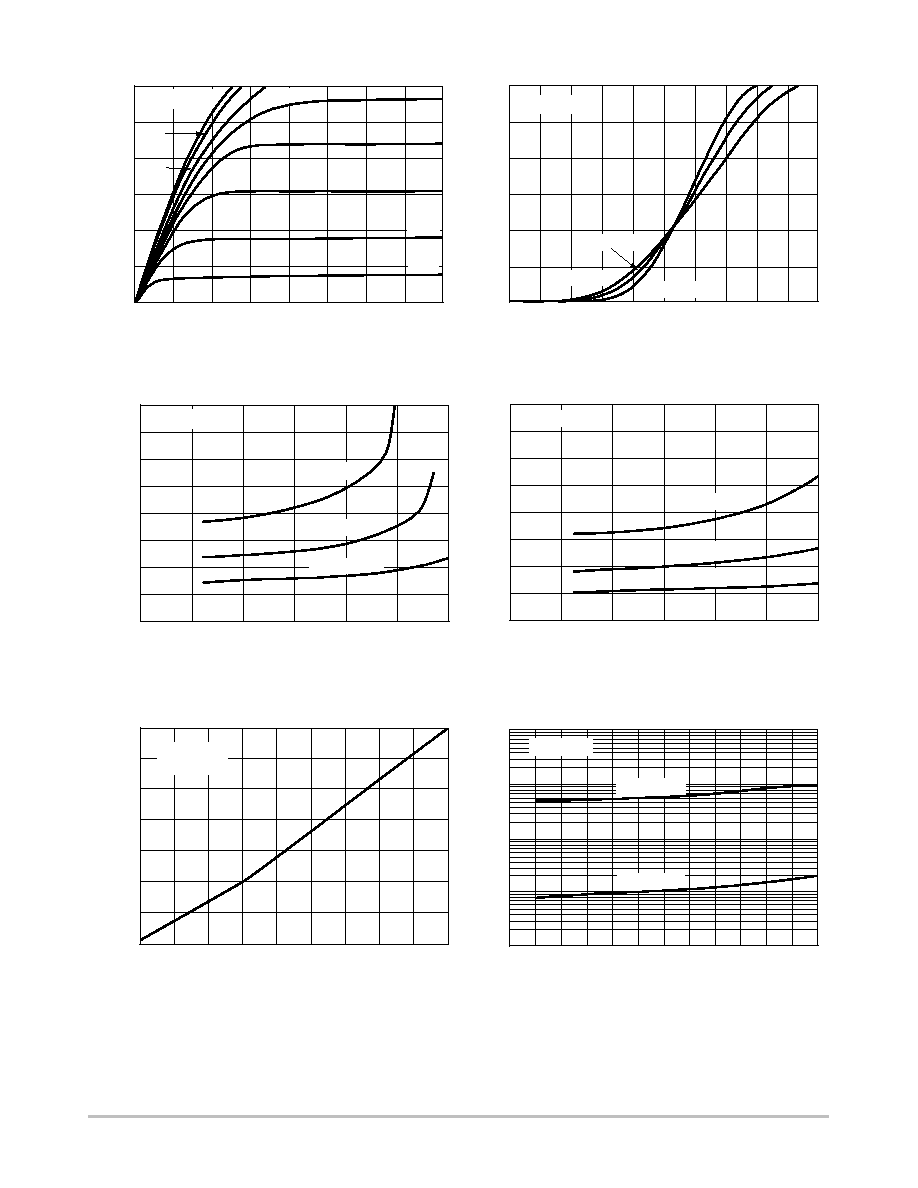
Figure 1. On-Region Characteristics
Figure 2. Transfer Characteristics
I
D
, DRAIN CURRENT (AMPS)
0
0.16
8
0.08
0
4
12
Figure 3. On-Resistance versus
Gate-to-Source Voltage
I
D
, DRAIN CURRENT (AMPS)
Figure 4. On-Resistance versus Drain Current
and Gate Voltage
I
D
, DRAIN CURRENT (AMPS)
R
DS(on)
, DRAIN-T
O-SOURCE RESIST
ANCE (
W
)
R
DS(on)
, DRAIN-T
O-SOURCE RESIST
ANCE (
W
)
Figure 5. On-Resistance Variation with
Temperature
T
J
, JUNCTION TEMPERATURE (
∞
C)
Figure 6. Drain-to-Source Leakage Current
versus Voltage
V
DS
, DRAIN-TO-SOURCE VOLTAGE (VOLTS)
R
DS(on)
, DRAIN-T
O-SOURCE RESIST
ANCE
(NORMALIZED)
I
DSS
, LEAKAGE (nA)
24
-50
50
25
0
-25
75
125
100
1
2.5
6
0
40
30
20
60
10
3
4
12
8 V
V
DS
10 V
T
J
= 25
∞
C
T
J
= -55
∞
C
T
J
= 100
∞
C
T
J
= 100
∞
C
V
GS
= 5 V
V
GS
= 10 V
150
175
V
GS
= 0 V
I
D
= 6 A
V
GS
= 5 V
16
0.32
V
GS
= 10 V
T
J
= 25
∞
C
T
J
= -55
∞
C
T
J
= 100
∞
C
24
T
J
= 150
∞
C
T
J
= 100
∞
C
0
24
8
16
3.5
4
T
J
= 25
∞
C
T
J
= -55
∞
C
50
10
6 V
4.5 V
4 V
3 V
1.8
4
5
6
7
1.5
2
3
4.5
5
5.5
0.24
16
20
0.24
0.28
2
20
5 V
3.5 V
4
0.20
0.16
1000
20
4
12
0.12
0.04
0.28
0.20
NTD3055L104
http://onsemi.com
4
POWER MOSFET SWITCHING
Switching behavior is most easily modeled and predicted
by recognizing that the power MOSFET is charge
controlled. The lengths of various switching intervals (
Dt)
are determined by how fast the FET input capacitance can
be charged by current from the generator.
The published capacitance data is difficult to use for
calculating rise and fall because drain-gate capacitance
varies greatly with applied voltage. Accordingly, gate
charge data is used. In most cases, a satisfactory estimate of
average input current (I
G(AV)
) can be made from a
rudimentary analysis of the drive circuit so that
t = Q/I
G(AV)
During the rise and fall time interval when switching a
resistive load, V
GS
remains virtually constant at a level
known as the plateau voltage, V
SGP
. Therefore, rise and fall
times may be approximated by the following:
t
r
= Q
2
x R
G
/(V
GG
- V
GSP
)
t
f
= Q
2
x R
G
/V
GSP
where
V
GG
= the gate drive voltage, which varies from zero to V
GG
R
G
= the gate drive resistance
and Q
2
and V
GSP
are read from the gate charge curve.
During the turn-on and turn-off delay times, gate current is
not constant. The simplest calculation uses appropriate
values from the capacitance curves in a standard equation for
voltage change in an RC network. The equations are:
t
d(on)
= R
G
C
iss
In [V
GG
/(V
GG
- V
GSP
)]
t
d(off)
= R
G
C
iss
In (V
GG
/V
GSP
)
The capacitance (C
iss
) is read from the capacitance curve at
a voltage corresponding to the off-state condition when
calculating t
d(on)
and is read at a voltage corresponding to the
on-state when calculating t
d(off)
.
At high switching speeds, parasitic circuit elements
complicate the analysis. The inductance of the MOSFET
source lead, inside the package and in the circuit wiring
which is common to both the drain and gate current paths,
produces a voltage at the source which reduces the gate drive
current. The voltage is determined by Ldi/dt, but since di/dt
is a function of drain current, the mathematical solution is
complex. The MOSFET output capacitance also
complicates the mathematics. And finally, MOSFETs have
finite internal gate resistance which effectively adds to the
resistance of the driving source, but the internal resistance
is difficult to measure and, consequently, is not specified.
The resistive switching time variation versus gate
resistance (Figure 9) shows how typical switching
performance is affected by the parasitic circuit elements. If
the parasitics were not present, the slope of the curves would
maintain a value of unity regardless of the switching speed.
The circuit used to obtain the data is constructed to minimize
common inductance in the drain and gate circuit loops and
is believed readily achievable with board mounted
components. Most power electronic loads are inductive; the
data in the figure is taken with a resistive load, which
approximates an optimally snubbed inductive load. Power
MOSFETs may be safely operated into an inductive load;
however, snubbing reduces switching losses.
C
rss
10
0
10
15
20
25
GATE-TO-SOURCE OR DRAIN-TO-SOURCE VOLTAGE (VOLTS)
C, CAP
ACIT
ANCE (pF)
Figure 7. Capacitance Variation
1000
200
0
V
GS
V
DS
400
5
5
V
GS
= 0 V
V
DS
= 0 V
T
J
= 25
∞
C
C
iss
C
oss
C
rss
C
iss
600
800
NTD3055L104
http://onsemi.com
5
16
0
0.3
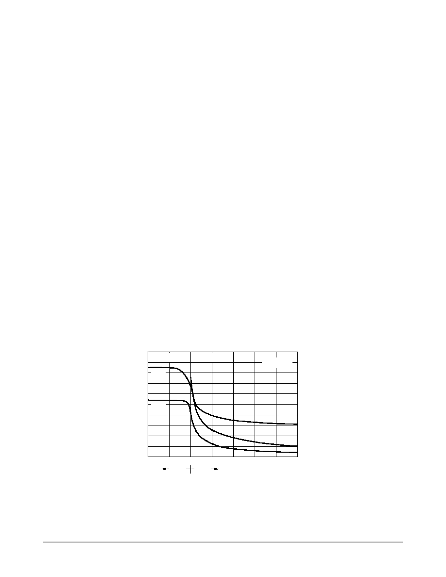
DRAIN-TO-SOURCE DIODE CHARACTERISTICS
V
SD
, SOURCE-TO-DRAIN VOLTAGE (VOLTS)
Figure 8. Gate-To-Source and Drain-To-Source
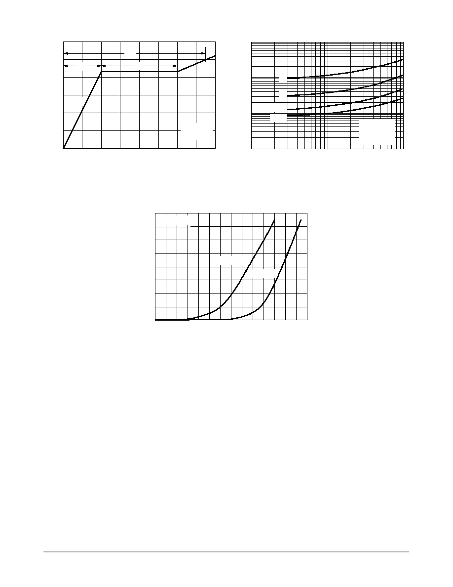
Voltage versus Total Charge
I S
, SOURCE CURRENT
(AMPS)
Figure 9. Resistive Switching Time
Variation versus Gate Resistance
R
G
, GATE RESISTANCE (OHMS)
1
10
100
1000
1
t, TIME
(ns)
V
GS
= 0 V
Figure 10. Diode Forward Voltage versus Current
V
GS
, GA
TE-T
O-SOURCE VOL
T
AGE (VOL
TS)
0
5
3
1
0
Q
G
, TOTAL GATE CHARGE (nC)
6
4
2
4
100
2
8
0.5
1
2
4
6
I
D
= 12 A
T
J
= 25
∞
C
V
GS
Q
2
Q
1
Q
T
t
r
t
d(off)
t
d(on)
t
f
10
V
DS
= 30 V
I
D
= 12 A
V
GS
= 5 V
0.7
0.9
6
8
0.8
0.6
0.4
10
12
14
T
J
= 150
∞
C
T
J
= 25
∞
C
SAFE OPERATING AREA
The Forward Biased Safe Operating Area curves define
the maximum simultaneous drain-to-source voltage and
drain current that a transistor can handle safely when it is
forward biased. Curves are based upon maximum peak
junction temperature and a case temperature (T
C
) of 25
∞
C.
Peak repetitive pulsed power limits are determined by using
the thermal response data in conjunction with the procedures
discussed in AN569, "Transient Thermal Resistance -
General Data and Its Use."
Switching between the off-state and the on-state may
traverse any load line provided neither rated peak current
(I
DM
) nor rated voltage (V
DSS
) is exceeded and the
transition time (t
r
,t
f
) do not exceed 10
ms. In addition the total
power averaged over a complete switching cycle must not
exceed (T
J(MAX)
- T
C
)/(R
qJC
).
A Power MOSFET designated E-FET can be safely used
in switching circuits with unclamped inductive loads. For
reliable operation, the stored energy from circuit inductance
dissipated in the transistor while in avalanche must be less
than the rated limit and adjusted for operating conditions
differing from those specified. Although industry practice is
to rate in terms of energy, avalanche energy capability is not
a constant. The energy rating decreases non-linearly with an
increase of peak current in avalanche and peak junction
temperature.
Although many E-FETs can withstand the stress of
drain-to-source avalanche at currents up to rated pulsed
current (I
DM
), the energy rating is specified at rated
continuous current (I
D
), in accordance with industry custom.
The energy rating must be derated for temperature as shown
in the accompanying graph (Figure 12). Maximum energy at
currents below rated continuous I
D
can safely be assumed to
equal the values indicated.