 | ÐлекÑÑоннÑй компоненÑ: NTD32N06L | СкаÑаÑÑ:  PDF PDF  ZIP ZIP |
Äîêóìåíòàöèÿ è îïèñàíèÿ www.docs.chipfind.ru
©
Semiconductor Components Industries, LLC, 2004
April, 2004 - Rev. 3
1
Publication Order Number:
NTD32N06L/D
NTD32N06L
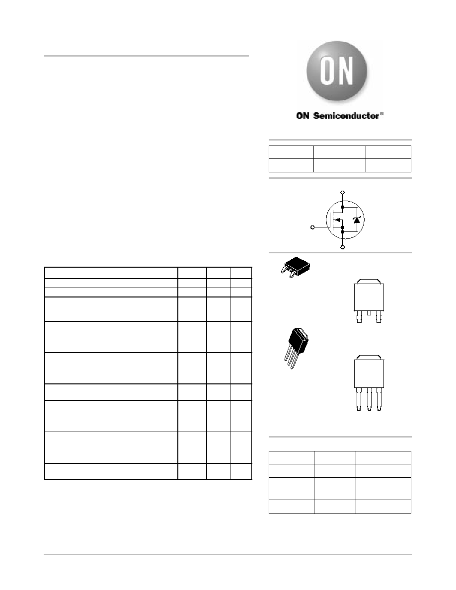
Power MOSFET
32 Amps, 60 Volts, Logic Level
N-Channel DPAK
Designed for low voltage, high speed switching applications in
power supplies, converters and power motor controls and bridge
circuits.
Features
·
Smaller Package than MTB30N06VL
·
Lower R
DS(on)
, V
DS(on)
, and Total Gate Charge
·
Lower and Tighter V
SD
·
Lower Diode Reverse Recovery Time
·
Lower Reverse Recovery Stored Charge
Typical Applications
·
Power Supplies
·
Converters
·
Power Motor Controls
·
Bridge Circuits
MAXIMUM RATINGS
(T
J
= 25
°
C unless otherwise noted)
Rating
Symbol
Value
Unit
Drain-to-Source Voltage
V
DSS
60
Vdc
Drain-to-Gate Voltage (R
GS
= 10 M
W
)
V
DGR
60
Vdc
Gate-to-Source Voltage
- Continuous
- Non-Repetitive (t
p
v
10 ms)
V
GS
V
GS
"
20
"
30
Vdc
Drain Current
- Continuous @ T
A
= 25
°
C
- Continuous @ T
A
= 100
°
C
- Single Pulse (t
p
v
10
m
s)
I
D
I
D
I
DM
32
22
90
Adc
Apk
Total Power Dissipation @ T
A
= 25
°
C
Derate above 25
°
C
Total Power Dissipation @ T
A
= 25
°
C (Note 1)
Total Power Dissipation @ T
A
= 25
°
C (Note 2)
P
D
93.75
0.625
2.88
1.5
W
W/
°
C
W
W
Operating and Storage Temperature Range
T
J
, T
stg
- 55 to
+175
°
C
Single Pulse Drain-to-Source Avalanche
Energy - Starting T
J
= 25
°
C (Note 3)
(V
DD
= 50 Vdc, V
GS
= 5 Vdc, L = 1.0 mH,
I
L(pk)
= 25 A, V
DS
= 60 Vdc, R
G
= 25
W
)
E
AS
313
mJ
Thermal Resistance
- Junction-to-Case
- Junction-to-Ambient (Note 1)
- Junction-to-Ambient (Note 2)
R
q
JC
R
q
JA
R
q
JA
1.6
52
100
°
C/W
Maximum Lead Temperature for Soldering
Purposes, 1/8
from case for 10 seconds
T
L
260
°
C
Maximum ratings are those values beyond which device damage can occur.
Maximum ratings applied to the device are individual stress limit values (not
normal operating conditions) and are not valid simultaneously. If these limits
are exceeded, device functional operation is not implied, damage may occur
and reliability may be affected.
1. When surface mounted to FR4 board using 0.5
pad size.
2. When surface mounted to FR4 board using minimum recommended pad
size.
3. Repetitive rating; pulse width limited by maximum junction temperature.
N-Channel
D
S
G
http://onsemi.com
2500/Tape & Reel
Device
Package
Shipping
ORDERING INFORMATION
NTD32N06L
DPAK
75 Units/Rail
NTD32N06L-1
DPAK
Straight Lead
75 Units/Rail
NTD32N06LT4
DPAK
1
Gate
3
Source
2
Drain
4
Drain
DPAK
CASE 369C
(Surface Mount)
Style 2
MARKING DIAGRAMS
32N06L
Device Code
Y
= Year
WW
= Work Week
YWW
32N06L
1 2
3
4
YWW
32N06L
1
Gate
3
Source
2
Drain
4
Drain
DPAK
CASE 369D
(Straight Lead)
Style 2
1
2
3
4
V
DSS
R
DS(ON)
TYP
I
D
MAX
60 V
23.7 m
W
32 A
For information on tape and reel specifications,
including part orientation and tape sizes, please
refer to our Tape and Reel Packaging Specifications
Brochure, BRD8011/D.
NTD32N06L
http://onsemi.com
2
ELECTRICAL CHARACTERISTICS
(T
J
= 25
°
C unless otherwise noted)
Characteristic
Symbol
Min
Typ
Max
Unit
OFF CHARACTERISTICS
Drain-to-Source Breakdown Voltage (Note 4)
(V
GS
= 0 Vdc, I
D
= 250
m
Adc)
Temperature Coefficient (Positive)
V
(BR)DSS
60
-
70
62
-
-
Vdc
mV/
°
C
Zero Gate Voltage Drain Current
(V
DS
= 60 Vdc, V
GS
= 0 Vdc)
(V
DS
= 60 Vdc, V
GS
= 0 Vdc, T
J
= 150
°
C)
I
DSS
-
-
-
-
1.0
10
m
Adc
Gate-Body Leakage Current (V
GS
=
±
20
Vdc, V
DS
= 0 Vdc)
I
GSS
-
-
±
100
nAdc
ON CHARACTERISTICS (Note 4)
Gate Threshold Voltage (Note 4)
(V
DS
= V
GS
, I
D
= 250
m
Adc)
Threshold Temperature Coefficient (Negative)
V
GS(th)
1.0
-
1.7
4.8
2.0
-
Vdc
mV/
°
C
Static Drain-to-Source On-Resistance (Note 4)
(V
GS
= 5 Vdc, I
D
= 16 Adc)
R
DS(on)
-
23.7
28
m
W
Static Drain-to-Source On-Resistance (Note 4)
(V
GS
= 5 Vdc, I
D
= 20 Adc)
(V
GS
= 5 Vdc, I
D
= 32 Adc)
(V
GS
= 5 Vdc, I
D
= 16 Adc, T
J
= 150
°
C)
V
DS(on)
-
-
-
0.48
0.78
0.61
0.67
-
-
Vdc
Forward Transconductance (Note 4) (V
DS
= 6 Vdc, I
D
= 16 Adc)
g
FS
-
27
-
mhos
DYNAMIC CHARACTERISTICS
Input Capacitance
C
iss
-
1214
1700
pF
Output Capacitance
(V
DS
= 25 Vdc, V
GS
= 0 Vdc,
f = 1.0 MHz)
C
oss
-
343
480
Transfer Capacitance
f = 1.0 MHz)
C
rss
-
87
180
SWITCHING CHARACTERISTICS (Note 5)
Turn-On Delay Time
t
d(on)
-
12.8
30
ns
Rise Time
(V
DD
= 30 Vdc, I
D
= 32 Adc,
V
GS
= 5 Vdc
t
r
-
221
450
Turn-Off Delay Time
V
GS
= 5 Vdc,
R
G
= 9.1
W
) (Note 4)
t
d(off)
-
37
80
Fall Time
G
) (
)
t
f
-
128
260
Gate Charge
Q
T
-
23
50
nC
(V
DS
= 48 Vdc, I
D
= 32 Adc,
V
GS
= 5 Vdc) (Note 4)
Q
1
-
4.5
-
V
GS
= 5 Vdc) (Note 4)
Q
2
-
14
-
SOURCE-DRAIN DIODE CHARACTERISTICS
Forward On-Voltage
(I
S
= 20 Adc, V
GS
= 0 Vdc) (Note 4)
(I
S
= 32 Adc, V
GS
= 0 Vdc) (Note 4)
(I
S
= 20 Adc, V
GS
= 0 Vdc, T
J
= 150
°
C)
V
SD
-
-
-
0.89
0.95
0.74
1.0
-
-
Vdc
Reverse Recovery Time
t
rr
-
56
-
ns
(I
S
= 32 Adc, V
GS
= 0 Vdc,
dI
S
/dt = 100 A/
m
s) (Note 4)
t
a
-
31
-
dI
S
/dt = 100 A/
m
s) (Note 4)
t
b
-
25
-
Reverse Recovery Stored Charge
Q
RR
-
0.093
-
m
C
4. Pulse Test: Pulse Width
300
m
s, Duty Cycle
2%.
5. Switching characteristics are independent of operating junction temperatures.
NTD32N06L
http://onsemi.com
3
1.8
1.6
1.2
1.4
1
0.8
0.6
100
10
1000
10000
40
20
50
10
30
0
60
0.026
0
50
4
20
2
1
V
DS
, DRAIN-TO-SOURCE VOLTAGE (VOLTS)
I
D
, DRAIN CURRENT (AMPS)
0
V
GS
, GATE-TO-SOURCE VOLTAGE (VOLTS)
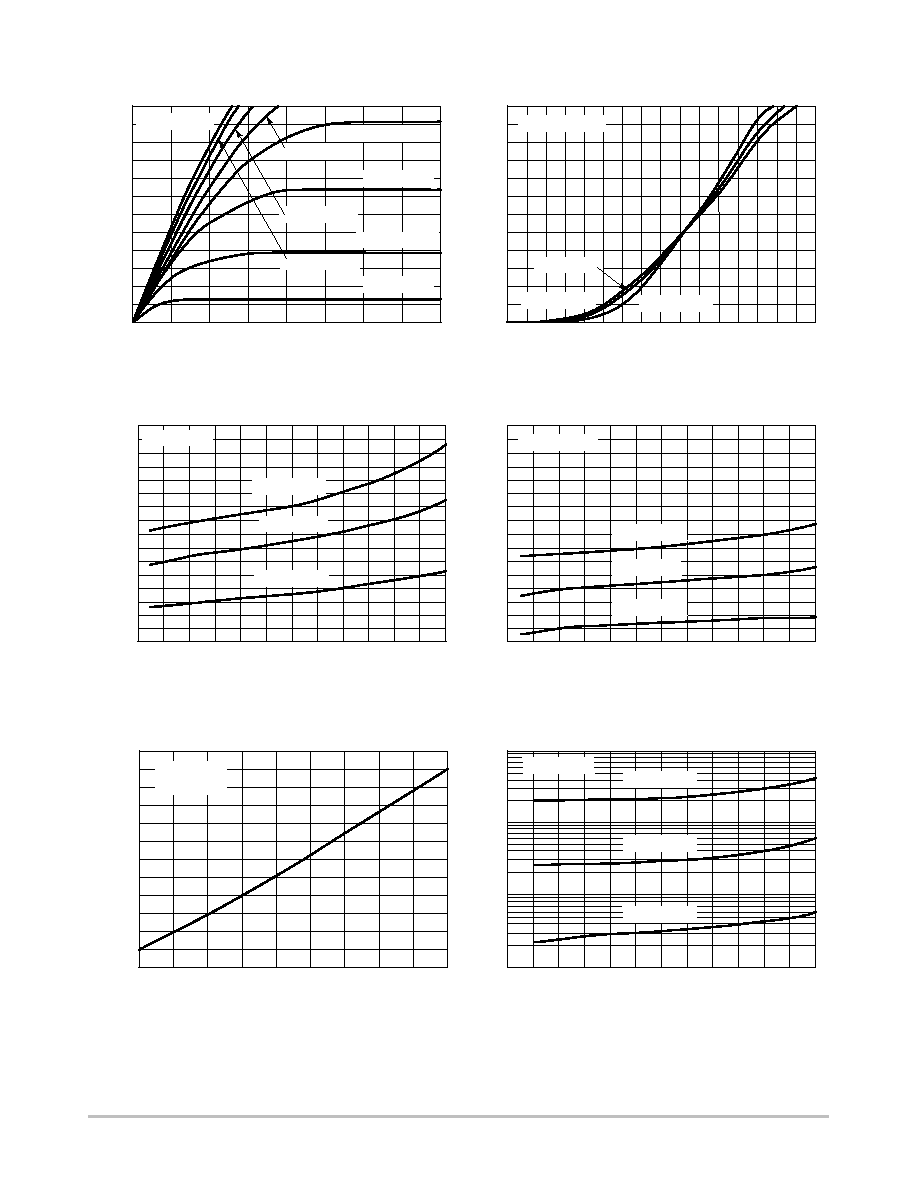
Figure 1. On-Region Characteristics
Figure 2. Transfer Characteristics
I
D
, DRAIN CURRENT (AMPS)
0
0.042
0.038
0.026
40
30
20
0.03
0.022
0.018
0.014
0.01
10
50
60
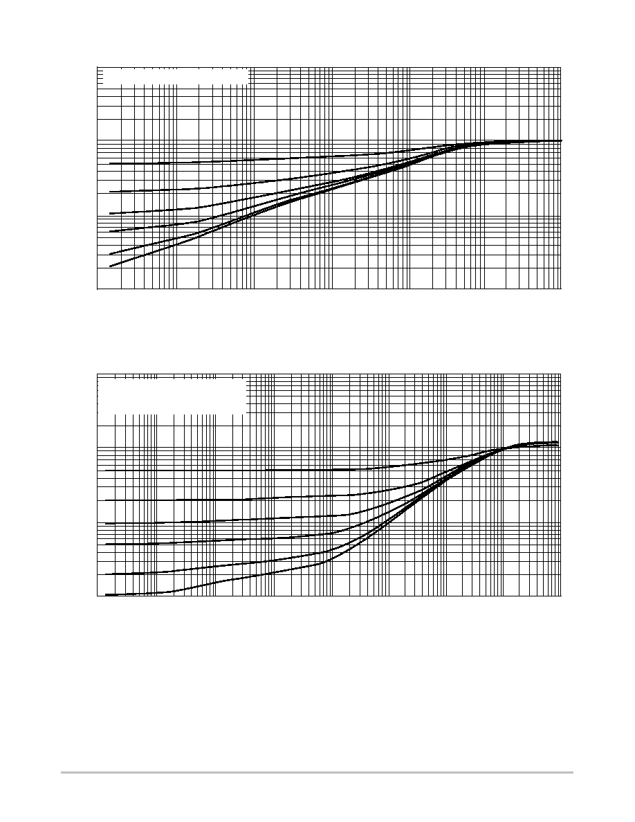
Figure 3. On-Resistance vs. Drain Current
I
D
, DRAIN CURRENT (AMPS)
Figure 4. On-Resistance vs. Drain Current
I
D
, DRAIN CURRENT (AMPS)
R
DS(on)
, DRAIN-T
O-SOURCE RESIST
ANCE (
W
)
R
DS(on)
, DRAIN-T
O-SOURCE RESIST
ANCE (
W
)
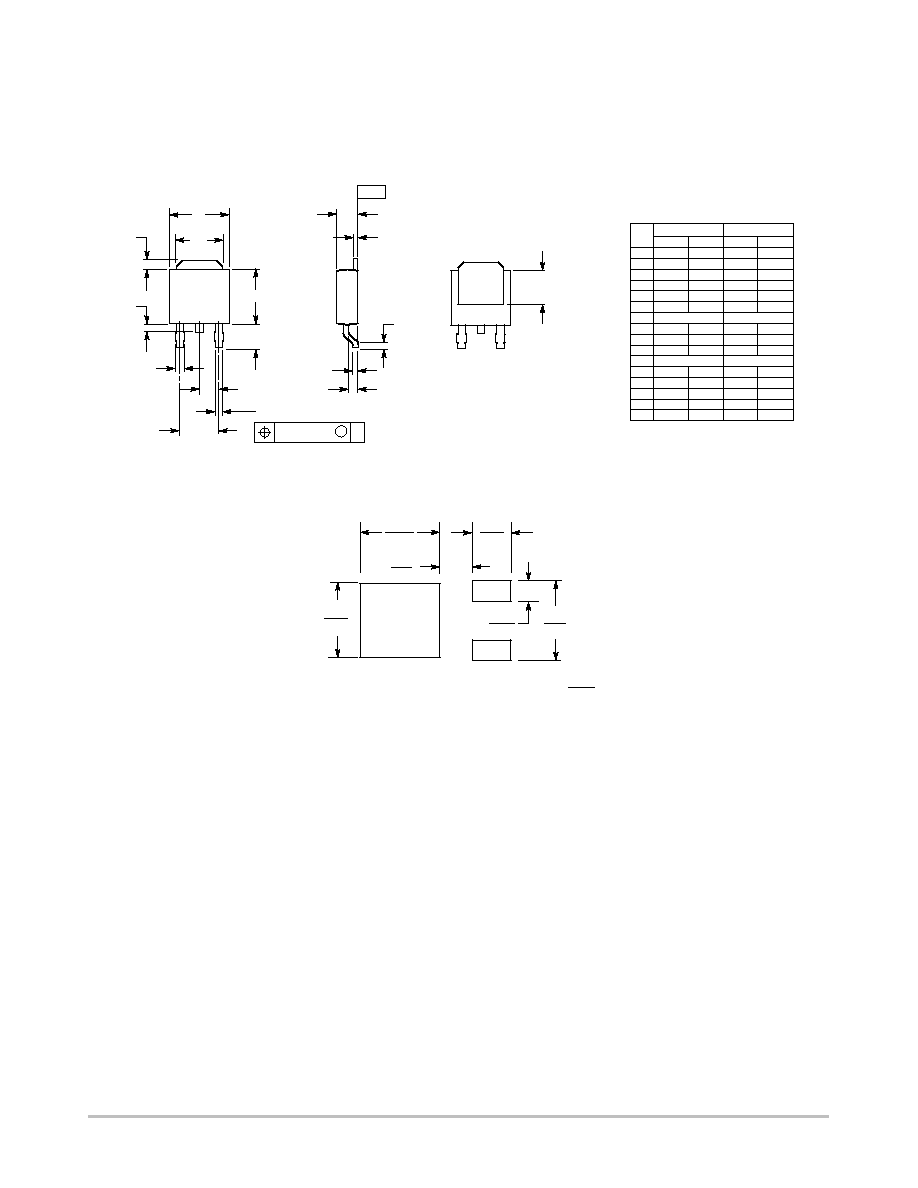
Figure 5. On-Resistance Variation with
Temperature
T
J
, JUNCTION TEMPERATURE (
°
C)
Figure 6. Drain-to-Source Leakage Current
vs. Voltage
V
DS
, DRAIN-TO-SOURCE VOLTAGE (VOLTS)
R
DS(on)
, DRAIN-T
O-SOURCE RESIST
ANCE
(NORMALIZED)
I
DSS
, LEAKAGE (nA)
60
-50
50
25
0
-25
75
125
100
1.8
3.4
3.8
3
2.6
4.2
2.2
5
0
30
40
20
50
10
60
0.01
0.03
0.022
0.018
0.034
0.042
0
40
50
30
20
60
10
V
GS
= 10 V
3
10
30
40
V
GS
= 8 V
V
GS
= 6 V
V
GS
= 5 V
V
GS
= 4.5 V
V
GS
= 4 V
V
GS
= 3.5 V
V
GS
= 3 V
V
DS
> = 10 V
T
J
= 25
°
C
T
J
= -55
°
C
T
J
= 100
°
C
4.6
T
J
= 25
°
C
T
J
= -55
°
C
T
J
= 100
°
C
V
GS
= 5 V
V
GS
= 10 V
150
175
V
GS
= 0 V
T
J
= 150
°
C
T
J
= 100
°
C
T
J
= 125
°
C
I
D
= 16 A
V
GS
= 5 V
0.014
0.038
0.034
T
J
= 25
°
C
T
J
= -55
°
C
T
J
= 100
°
C
NTD32N06L
http://onsemi.com
4
1000
100
10
1
0.1
1000
100
10
6
5
4
3
2
1
0
350
150
100
50
0
32
28
24
20
16
12
0
10
3200
2800
10
2400
2000
15
5
0
20
GATE-TO-SOURCE OR DRAIN-TO-SOURCE VOLTAGE
(VOLTS)
C, CAP
ACIT
ANCE (pF)
1600
1200
800
400
0
5
Q
g
, TOTAL GATE CHARGE (nC)
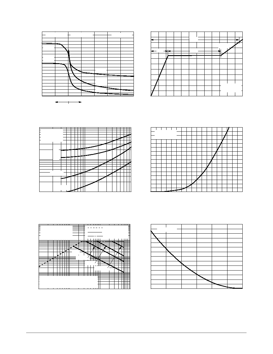
Figure 7. Capacitance Variation
Figure 8. Gate-to-Source and
Drain-to-Source Voltage vs. Total Charge
V
GS
, GA
TE-T
O-SOURCE VOL
T
AGE (VOL
TS)
Figure 9. Resistive Switching Time Variation
vs. Gate Resistance
R
G
, GATE RESISTANCE (
W
)
Figure 10. Diode Forward Voltage vs. Current
V
SD
, SOURCE-TO-DRAIN VOLTAGE (VOLTS)
I
S
, SOURCE CURRENT (AMPS)
t, TIME (ns)
Figure 11. Maximum Rated Forward Biased
Safe Operating Area
V
DS
, DRAIN-TO-SOURCE VOLTAGE (VOLTS)
Figure 12. Maximum Avalanche Energy vs.
Starting Junction Temperature
T
J
, STARTING JUNCTION TEMPERATURE (
°
C)
I
D
, DRAIN CURRENT (AMPS)
E
AS
, SINGLE PULSE DRAIN-T
O-SOURCE
A
V
ALANCHE ENERGY (mJ)
25
0
16
20
12
8
24
4
1
10
100
0.6
0.76
0.88
0.72
0.68
0.92
0.64
0.96
0.1
10
100
1
25
125
150
100
75
175
50
I
D
= 32 A
T
J
= 25
°
C
V
GS
V
GS
= 0 V
V
DS
= 0 V
T
J
= 25
°
C
C
rss
C
iss
C
oss
C
rss
8
4
0.8
0.84
Q
2
C
iss
V
GS
= 20 V
SINGLE PULSE
T
C
= 25
°
C
V
DS
= 30 V
I
D
= 32 A
V
GS
= 5 V
V
GS
= 0 V
T
J
= 25
°
C
I
D
= 32 A
10 ms
1 ms
100
m
s
dc
t
r
t
d(off)
t
d(on)
t
f
V
GS
V
DS
Q
1
200
250
300
4000
Mounted on 3
sq. FR4 board (1
sq.
2 oz. Cu 0.06
thick single sided)
with one die operating,10 s max
Q
T
R
DS(on)
Limit
Thermal Limit
Package Limit
3600
NTD32N06L
http://onsemi.com
5
10
0.1
0.01
0.00001
0.0001
r(t)
, EFFECTIVE TRANSIENT THERMAL RESPONSE
(NORMALIZED)
t, TIME (s)
Figure 13. Thermal Response
1
0.001
0.01
0.1
1
10
100
1000
10
0.1
0.01
0.00001
0.0001
r(t)
, EFFECTIVE TRANSIENT THERMAL RESIST
ANCE
(NORMALIZED)
t, TIME (s)
1
0.001
0.01
0.1
1
10
Figure 14. Thermal Response
Normalized to R
q
JC
at Steady State
Normalized to R
q
JA
at Steady State,
1
square Cu Pad, Cu Area 1.127 in
2
,
3 x 3 inch FR4 board
NTD32N06L
http://onsemi.com
6
PACKAGE DIMENSIONS
DPAK-3
CASE 369C-01
ISSUE O
D
A
K
B
R
V
S
F
L
G
2 PL
M
0.13 (0.005)
T
E
C
U
J
H
-T-
SEATING
PLANE
Z
DIM
MIN
MAX
MIN
MAX
MILLIMETERS
INCHES
A
0.235
0.245
5.97
6.22
B
0.250
0.265
6.35
6.73
C
0.086
0.094
2.19
2.38
D
0.027
0.035
0.69
0.88
E
0.018
0.023
0.46
0.58
F
0.037
0.045
0.94
1.14
G
0.180 BSC
4.58 BSC
H
0.034
0.040
0.87
1.01
J
0.018
0.023
0.46
0.58
K
0.102
0.114
2.60
2.89
L
0.090 BSC
2.29 BSC
R
0.180
0.215
4.57
5.45
S
0.025
0.040
0.63
1.01
U
0.020
---
0.51
---
V
0.035
0.050
0.89
1.27
Z
0.155
---
3.93
---
1
2
3
4
STYLE 2:
PIN 1. GATE
2. DRAIN
3. SOURCE
4. DRAIN
5.80
0.228
2.58
0.101
1.6
0.063
6.20
0.244
3.0
0.118
6.172
0.243
mm
inches
SCALE 3:1
SOLDERING FOOTPRINT
NTD32N06L
http://onsemi.com
7
PACKAGE DIMENSIONS
DPAK-3
CASE 369D-01
ISSUE B
STYLE 2:
PIN 1. GATE
2. DRAIN
3. SOURCE
4. DRAIN
1
2
3
4
V
S
A
K
-T-
SEATING
PLANE
R
B
F
G
D
3 PL
M
0.13 (0.005)
T
C
E
J
H
DIM
MIN
MAX
MIN
MAX
MILLIMETERS
INCHES
A
0.235
0.245
5.97
6.35
B
0.250
0.265
6.35
6.73
C
0.086
0.094
2.19
2.38
D
0.027
0.035
0.69
0.88
E
0.018
0.023
0.46
0.58
F
0.037
0.045
0.94
1.14
G
0.090 BSC
2.29 BSC
H
0.034
0.040
0.87
1.01
J
0.018
0.023
0.46
0.58
K
0.350
0.380
8.89
9.65
R
0.180
0.215
4.45
5.45
S
0.025
0.040
0.63
1.01
V
0.035
0.050
0.89
1.27
NOTES:
1. DIMENSIONING AND TOLERANCING PER
ANSI Y14.5M, 1982.
2. CONTROLLING DIMENSION: INCH.
Z
Z
0.155
---
3.93
---

NTD32N06L
http://onsemi.com
8
ON Semiconductor and are registered trademarks of Semiconductor Components Industries, LLC (SCILLC). SCILLC reserves the right to make changes without further notice
to any products herein. SCILLC makes no warranty, representation or guarantee regarding the suitability of its products for any particular purpose, nor does SCILLC assume any liability
arising out of the application or use of any product or circuit, and specifically disclaims any and all liability, including without limitation special, consequential or incidental damages.
"Typical" parameters which may be provided in SCILLC data sheets and/or specifications can and do vary in different applications and actual performance may vary over time. All
operating parameters, including "Typicals" must be validated for each customer application by customer's technical experts. SCILLC does not convey any license under its patent rights
nor the rights of others. SCILLC products are not designed, intended, or authorized for use as components in systems intended for surgical implant into the body, or other applications
intended to support or sustain life, or for any other application in which the failure of the SCILLC product could create a situation where personal injury or death may occur. Should
Buyer purchase or use SCILLC products for any such unintended or unauthorized application, Buyer shall indemnify and hold SCILLC and its officers, employees, subsidiaries, affiliates,
and distributors harmless against all claims, costs, damages, and expenses, and reasonable attorney fees arising out of, directly or indirectly, any claim of personal injury or death
associated with such unintended or unauthorized use, even if such claim alleges that SCILLC was negligent regarding the design or manufacture of the part. SCILLC is an Equal
Opportunity/Affirmative Action Employer. This literature is subject to all applicable copyright laws and is not for resale in any manner.
PUBLICATION ORDERING INFORMATION
N. American Technical Support: 800-282-9855 Toll Free
USA/Canada
Japan: ON Semiconductor, Japan Customer Focus Center
2-9-1 Kamimeguro, Meguro-ku, Tokyo, Japan 153-0051
Phone: 81-3-5773-3850
NTD32N06L/D
LITERATURE FULFILLMENT:
Literature Distribution Center for ON Semiconductor
P.O. Box 5163, Denver, Colorado 80217 USA
Phone: 303-675-2175 or 800-344-3860 Toll Free USA/Canada
Fax: 303-675-2176 or 800-344-3867 Toll Free USA/Canada
Email: orderlit@onsemi.com
ON Semiconductor Website: http://onsemi.com
Order Literature: http://www.onsemi.com/litorder
For additional information, please contact your
local Sales Representative.