 | –≠–ª–µ–∫—Ç—Ä–æ–Ω–Ω—ã–π –∫–æ–º–ø–æ–Ω–µ–Ω—Ç: NTD4810N | –°–∫–∞—á–∞—Ç—å:  PDF PDF  ZIP ZIP |
©
Semiconductor Components Industries, LLC, 2006
February, 2006 - Rev. 0
1
Publication Order Number:
NTD4810N/D
NTD4810N
Power MOSFET
30 V, 54 A, Single N-Channel, DPAK/IPAK
Features
∑
Low R
DS(on)
to Minimize Conduction Losses
∑
Low Capacitance to Minimize Driver Losses
∑
Optimized Gate Charge to Minimize Switching Losses
∑
These are Pb-Free Devices
Applications
∑
CPU Power Delivery
∑
DC-DC Converters
MAXIMUM RATINGS
(T
J
= 25
∞
C unless otherwise noted)
Parameter
Symbol
Value
Unit
Drain-to-Source Voltage
V
DSS
30
V
Gate-to-Source Voltage
V
GS
"
20
V
Continuous Drain
Current (R
q
JA
) (Note 1)
Steady
State
T
A
= 25
∞
C
I
D
10.8
A
T
A
= 85
∞
C
8.4
Power Dissipation
(R
q
JA
) (Note 1)
T
A
= 25
∞
C
P
D
2.0
W
Continuous Drain
Current (R
q
JA
) (Note 2)
T
A
= 25
∞
C
I
D
8.6
A
T
A
= 85
∞
C
6.7
Power Dissipation
(R
q
JA
) (Note 2)
T
A
= 25
∞
C
P
D
1.28
W
Continuous Drain
Current (R
q
JC
)
(Note 1)
T
C
= 25
∞
C
I
D
54
A
T
C
= 85
∞
C
42
Power Dissipation
(R
q
JC
) (Note 1)
T
C
= 25
∞
C
P
D
50
W
Pulsed Drain Current
t
p
=10
m
s
T
A
= 25
∞
C
I
DM
120
A
Current Limited by Package
T
A
= 25
∞
C
I
DmaxPkg
45
A
Operating Junction and Storage Temperature
T
J
, T
stg
- 55 to
175
∞
C
Source Current (Body Diode)
I
S
41
A
Drain to Source dV/dt
dV/dt
6.0
V/ns
Single Pulse Drain-to-Source Avalanche
Energy (V
DD
= 30 V, V
GS
= 10 V,
L = 1.0 mH, I
L(pk)
= 14 A, R
G
= 25
W
)
E
AS
98
mJ
Lead Temperature for Soldering Purposes
(1/8
from case for 10 s)
T
L
260
∞
C
Maximum ratings are those values beyond which device damage can occur.
Maximum ratings applied to the device are individual stress limit values (not
normal operating conditions) and are not valid simultaneously. If these limits are
exceeded, device functional operation is not implied, damage may occur and
reliability may be affected.
CASE 369C
DPAK
(Bend Lead)
STYLE 2
MARKING DIAGRAMS
& PIN ASSIGNMENTS
CASE 369D
DPAK
(Straight Lead)
STYLE 2
30 V
10 m
W
@ 10 V
R
DS(on)
MAX
54 A
I
D
MAX
V
(BR)DSS
15.7 m
W
@ 4.5 V
http://onsemi.com
1 2
3
4
See detailed ordering and shipping information in the package
dimensions section on page 6 of this data sheet.
ORDERING INFORMATION
1
2
3
4
CASE 369AC
3 IPAK
(Straight Lead)
1
2
3
4
N-Channel
D
S
G
YWW
4810NG
1
Gate
2
Drain 3
Source
4
Drain
4
Drain
2
Drain
1
Gate
3
Source
4
Drain
2
Drain
1
Gate
3
Source
YWW
4810NG
YWW
4810NG
Y
= Year
WW
= Work Week
4810N = Device Code
G
= Pb-Free Package
NTD4810N
http://onsemi.com
2
THERMAL RESISTANCE MAXIMUM RATINGS
Parameter
Symbol
Value
Unit
Junction-to-Case (Drain)
R
q
JC
3.0
∞
C/W
Junction-to-TAB (Drain)
R
q
JC-TAB
3.5
Junction-to-Ambient - Steady State (Note 1)
R
q
JA
75
Junction-to-Ambient - Steady State (Note 2)
R
q
JA
117
1. Surface-mounted on FR4 board using 1 in sq pad size, 1 oz Cu.
2. Surface-mounted on FR4 board using the minimum recommended pad size.
ELECTRICAL CHARACTERISTICS
(T
J
= 25
∞
C unless otherwise noted)
Parameter
Symbol
Test Condition
Min
Typ
Max
Unit
OFF CHARACTERISTICS
Drain-to-Source Breakdown Voltage
V
(BR)DSS
V
GS
= 0 V, I
D
= 250
m
A
30
V
Drain-to-Source Breakdown Voltage
Temperature Coefficient
V
(BR)DSS
/T
J
27
mV/
∞
C
Zero Gate Voltage Drain Current
I
DSS
V
GS
= 0 V,
V
DS
= 24 V
T
J
= 25
∞
C
1.0
m
A
T
J
= 125
∞
C
10
Gate-to-Source Leakage Current
I
GSS
V
DS
= 0 V, V
GS
=
"
20 V
"
100
nA
ON CHARACTERISTICS (Note 3)
Gate Threshold Voltage
V
GS(TH)
V
GS
= V
DS
, I
D
= 250
m
A
1.5
2.5
V
Negative Threshold Temperature Coefficient
V
GS(TH)
/T
J
5.2
mV/
∞
C
Drain-to-Source On Resistance
R
DS(on)
V
GS
= 10 to
11.5 V
I
D
= 30 A
8.0
10
m
W
I
D
= 15 A
7.8
V
GS
= 4.5 V
I
D
= 30 A
12
15.7
I
D
= 15 A
11
Forward Transconductance
gFS
V
DS
= 15 V, I
D
= 15 A
9.0
S
CHARGES AND CAPACITANCES
Input Capacitance
C
iss
V
GS
= 0 V, f = 1.0 MHz,
V
DS
= 12 V
1165
pF
Output Capacitance
C
oss
284
Reverse Transfer Capacitance
C
rss
154
Total Gate Charge
Q
G(TOT)
V
GS
= 4.5 V, V
DS
= 15 V,
I
D
= 30 A
9.0
11
nC
Threshold Gate Charge
Q
G(TH)
1.3
Gate-to-Source Charge
Q
GS
3.3
Gate-to-Drain Charge
Q
GD
4.4
Total Gate Charge
Q
G(TOT)
V
GS
= 11.5 V, V
DS
= 15 V,
I
D
= 30 A
21
nC
SWITCHING CHARACTERISTICS (Note 4)
Turn-On Delay Time
t
d(on)
V
GS
= 4.5 V, V
DS
= 15 V,
I
D
= 30 A, R
G
= 3.0
W
11
ns
Rise Time
t
r
88
Turn-Off Delay Time
t
d(off)
11
Fall Time
t
f
5.4
Turn-On Delay Time
t
d(on)
V
GS
= 11.5 V, V
DS
= 15 V,
I
D
= 30 A, R
G
= 3.0
W
4.9
ns
Rise Time
t
r
18.2
Turn-Off Delay Time
t
d(off)
19.7
Fall Time
t
f
3.2
3. Pulse Test: Pulse Width
300
m
s, Duty Cycle
2%.
4. Switching characteristics are independent of operating junction temperatures.
NTD4810N
http://onsemi.com
3
ELECTRICAL CHARACTERISTICS
(T
J
= 25
∞
C unless otherwise noted)
Parameter
Symbol
Test Condition
Min
Typ
Max
Unit
DRAIN-SOURCE DIODE CHARACTERISTICS
Forward Diode Voltage
V
SD
V
GS
= 0 V,
I
S
= 30 A
T
J
= 25
∞
C
0.92
1.2
V
T
J
= 125
∞
C
0.79
Reverse Recovery Time
t
RR
V
GS
= 0 V, dIs/dt = 100 A/
m
s,
I
S
= 30 A
18.2
ns
Charge Time
ta
10.6
Discharge Time
tb
7.6
Reverse Recovery Time
Q
RR
8.8
nC
PACKAGE PARASITIC VALUES
Source Inductance
L
S
T
A
= 25
∞
C
2.49
nH
Drain Inductance, DPAK
L
D
0.0164
Drain Inductance, IPAK
L
D
1.88
Gate Inductance
L
G
3.46
Gate Resistance
R
G
2.4
W
NTD4810N
http://onsemi.com
4
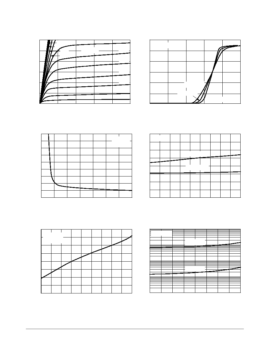
TYPICAL PERFORMANCE CURVES
4 V
10 V
10
0.020
30
0.005
0
1.5
1.0
0
10,000
100,000
0
5
30
2
1
V
DS
, DRAIN-TO-SOURCE VOLTAGE (VOLTS)
I
D
, DRAIN CURRENT (AMPS)
0
V
GS
, GATE-TO-SOURCE VOLTAGE (VOLTS)
Figure 1. On-Region Characteristics
Figure 2. Transfer Characteristics
I
D
, DRAIN CURRENT (AMPS)
3
0.048
4
0.023
0.013
0.003
5
Figure 3. On-Resistance vs. Gate-to-Source
Voltage
V
GS
, GATE-TO-SOURCE VOLTAGE (VOLTS)
Figure 4. On-Resistance vs. Drain Current and
Gate Voltage
I
D
, DRAIN CURRENT (AMPS)
R
DS(on)
, DRAIN-T
O-SOURCE RESIST
ANCE (
W
)
R
DS(on)
, DRAIN-T
O-SOURCE RESIST
ANCE (
W
)
Figure 5. On-Resistance Variation with
Temperature
T
J
, JUNCTION TEMPERATURE (
∞
C)
Figure 6. Drain-to-Source Leakage Current
vs. Drain Voltage
V
DS
, DRAIN-TO-SOURCE VOLTAGE (VOLTS)
R
DS(on)
, DRAIN-T
O-SOURCE RESIST
ANCE
(NORMALIZED)
I
DSS
, LEAKAGE (nA)
-50
50
25
0
-25
75
125
100
2
3
15
10
25
5
3
V
DS
10 V
T
J
= 25
∞
C
T
J
= -55
∞
C
T
J
= 125
∞
C
V
GS
= 4.5 V
175
V
GS
= 0 V
I
D
= 30 A
V
GS
= 10 V
50
T
J
= 175
∞
C
T
J
= 125
∞
C
40
0
4
5
T
J
= 25
∞
C
20
10
5 V
3 V
6 V
2.0
1000
4
1
0
6
10
0.033
40
0.010
50
4.5 V
3.4 V
3.6 V
3.8 V
40
10
20
60
30
20
60
10
50
I
D
= 30 A
T
J
= 25
∞
C
7
8
9
0.008
0.018
0.028
0.043
0.038
25
35
45
55
V
GS
= 11.5 V
150
100
3.2 V
T
J
= 25
∞
C
0.015
15
20
2.8 V
0.5
NTD4810N
http://onsemi.com
5
TYPICAL PERFORMANCE CURVES
C
rss
10
0
10
15
25
GATE-TO-SOURCE OR DRAIN-TO-SOURCE VOLTAGE (VOLTS)
C, CAP
ACIT
ANCE (pF)
Figure 7. Capacitance Variation
1000
0
V
GS
V
DS
2000
5
5
V
GS
= 0 V
V
DS
= 0 V
T
J
= 25
∞
C
C
iss
C
oss
C
rss
C
iss
1500
Figure 8. Gate-To-Source and Drain-To-Source
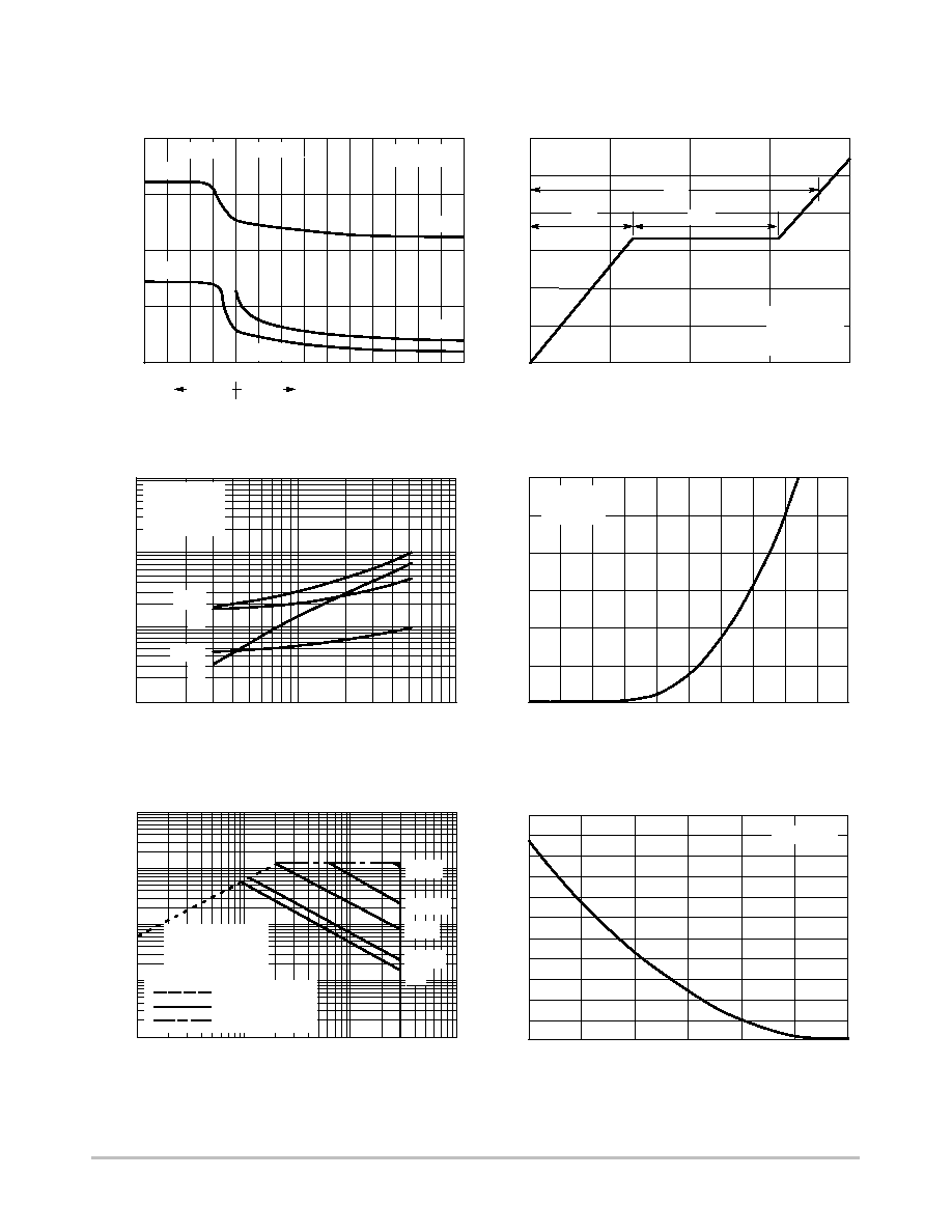
Voltage vs. Total Charge
V
GS
, GA
TE-T
O-SOURCE VOL
T
AGE (VOL
TS
)
0
2
0
Q
G
, TOTAL GATE CHARGE (nC)
1
4
7.5
5
I
D
= 30 A
V
GS
= 4.5 V
T
J
= 25
∞
C
Q
2
Q
1
Q
T
10
0
0.5
V
SD
, SOURCE-TO-DRAIN VOLTAGE (VOLTS)
I S
, SOURCE CURRENT
(AMPS)
Figure 9. Resistive Switching Time
Variation vs. Gate Resistance
R
G
, GATE RESISTANCE (OHMS)
1
10
100
1000
1
t, TIME
(ns)
V
GS
= 0 V
Figure 10. Diode Forward Voltage vs. Current
100
0.6
0.7
1.0
5
10
15
t
r
t
d(off)
t
d(on)
t
f
10
V
DD
= 15 V
I
D
= 30 A
V
GS
= 11.5 V
0.8
0.9
20
30
25
T
J
= 25
∞
C
Figure 11. Maximum Rated Forward Biased
Safe Operating Area
0.1
1
100
V
DS
, DRAIN-TO-SOURCE VOLTAGE (VOLTS)
0.1
1000
I D
, DRAIN CURRENT
(AMPS)
R
DS(on)
LIMIT
THERMAL LIMIT
PACKAGE LIMIT
10
10
V
GS
= 20 V
SINGLE PULSE
T
C
= 25
∞
C
1 ms
100
m
s
10 ms
dc
10
m
s
20
6
1
100
0
25
T
J
, JUNCTION TEMPERATURE (
∞
C)
I
D
= 14 A
Figure 12. Maximum Avalanche Energy vs.
Starting Junction Temperature
50
75
175
20
60
80
100
125
100
110
EAS, SINGLE PULSE DRAIN-T
O-SOURCE
A
V
ALANCHE ENERGY (mJ)
150
500
40
2.5
3
5
10
50
70
90
30