
Publication Order Number:
NTF3055L108/D
©
Semiconductor Components Industries, LLC, 2005
December, 2005 - Rev. 4
1
NTF3055L108
Preferred Device
Power MOSFET
3.0 A, 60 V, Logic Level, N-Channel
SOT-223
Designed for low voltage, high speed switching applications in
power supplies, converters and power motor controls and bridge
circuits.
Features
∑
Pb-Free Packages are Available
Applications
∑
Power Supplies
∑
Converters
∑
Power Motor Controls
∑
Bridge Circuits
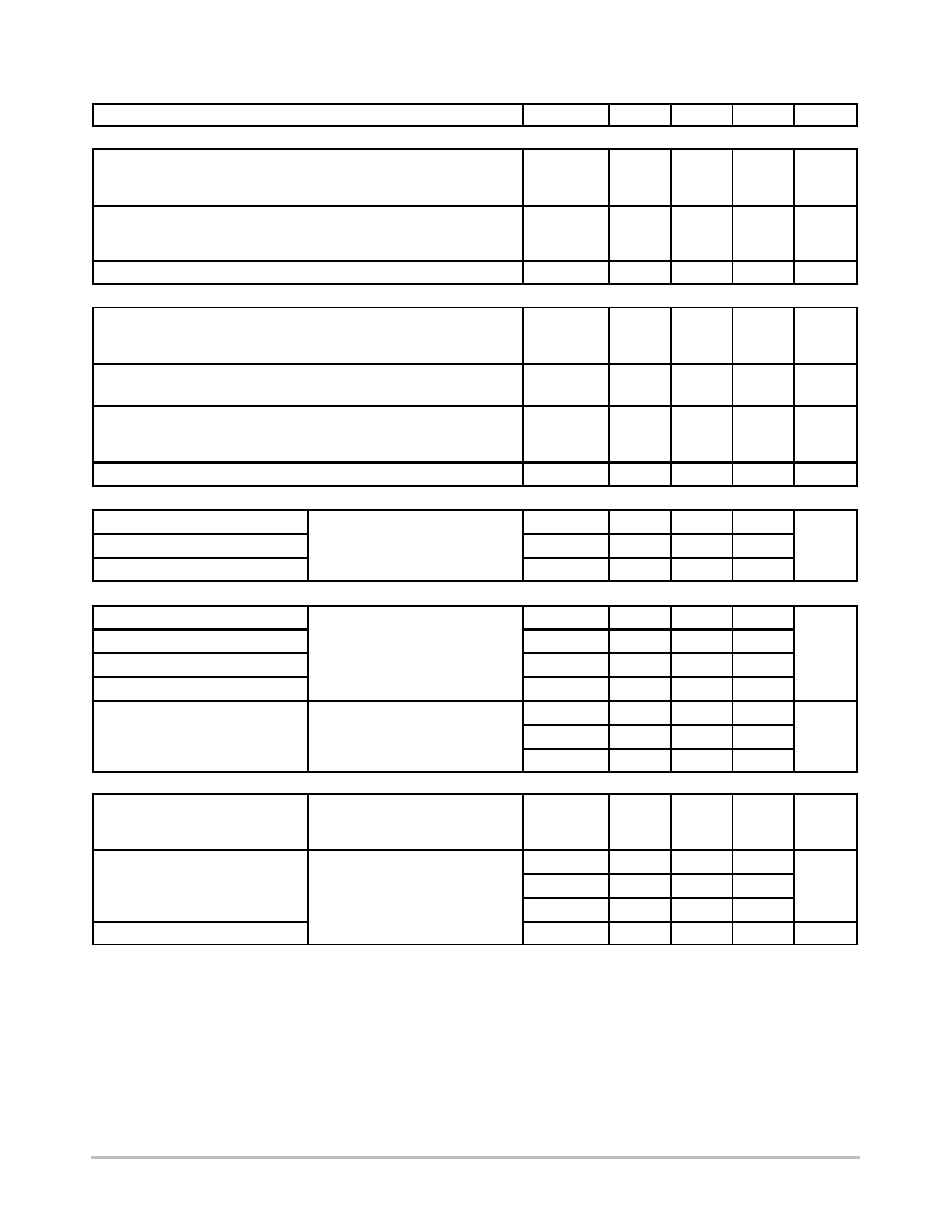
MAXIMUM RATINGS
(T
C
= 25
∞
C unless otherwise noted)
Rating
Symbol
Value
Unit
Drain-to-Source Voltage
V
DSS
60
Vdc
Drain-to-Gate Voltage (R
GS
= 1.0 M
W
)
V
DGR
60
Vdc
Gate-to-Source Voltage
- Continuous
- Non-repetitive (t
p
10 ms)
V
GS
±
15
±
20
Vdc
Vpk
Drain Current
- Continuous @ T
A
= 25
∞
C
- Continuous @ T
A
= 100
∞
C
- Single Pulse (t
p
10
m
s)
I
D
I
D
I
DM
3.0
1.4
9.0
Adc
Apk
Total Power Dissipation @ T
A
= 25
∞
C (Note 1)
Total Power Dissipation @ T
A
= 25
∞
C (Note 2)
Derate above 25
∞
C
P
D
2.1
1.3
0.014
Watts
Watts
W/
∞
C
Operating and Storage Temperature Range
T
J
, T
stg
- 55
to 175
∞
C
Single Pulse Drain-to-Source Avalanche
Energy - Starting T
J
= 25
∞
C
(V
DD
= 25 Vdc, V
GS
= 5.0 Vdc,
I
L(pk)
= 7.0 Apk, L = 3.0 mH, V
DS
= 60 Vdc)
E
AS
74
mJ
Thermal Resistance
-Junction-to-Ambient (Note 1)
-Junction-to-Ambient (Note 2)
R
q
JA
R
q
JA
72.3
114
∞
C/W
Maximum Lead Temperature for Soldering
Purposes, 1/8
from case for 10 seconds
T
L
260
∞
C
Maximum ratings are those values beyond which device damage can occur.
Maximum ratings applied to the device are individual stress limit values (not
normal operating conditions) and are not valid simultaneously. If these limits are
exceeded, device functional operation is not implied, damage may occur and
reliability may be affected.
1. When surface mounted to an FR4 board using 1
pad size, 1 oz.
(Cu. Area 0.0995 in
2
).
2. When surface mounted to an FR4 board using minimum recommended pad
size, 2-2.4 oz. (Cu. Area 0.272 in
2
).
D
G
S
1
2
3
4
3.0 A, 60 V
R
DS(on)
= 120 m
W
N-Channel
SOT-223
CASE 318E
STYLE 3
MARKING DIAGRAM
AYW
3055L
G
G
3055L
= Device Code
A
= Assembly Location
Y
= Year
W
= Work Week
G
= Pb-Free Package
(Note: Microdot may be in either location)
PIN ASSIGNMENT
3
2
1
4
Gate
Drain Source
Drain
Preferred devices are recommended choices for future use
and best overall value.
See detailed ordering and shipping information in the package
dimensions section on page 5 of this data sheet.
ORDERING INFORMATION
http://onsemi.com
NTF3055L108
http://onsemi.com
2
ELECTRICAL CHARACTERISTICS
(T
A
= 25
∞
C unless otherwise noted)
Characteristic
Symbol
Min
Typ
Max
Unit
OFF CHARACTERISTICS
Drain-to-Source Breakdown Voltage
(Note 3)
(V
GS
= 0 Vdc,
I
D
= 250
m
Adc)
Temperature Coefficient (Positive)
V
(BR)DSS
60
-
68
68
-
-
Vdc
mV/
∞
C
Zero Gate Voltage Drain Current
(V
DS
= 60 Vdc, V
GS
= 0 Vdc)
(V
DS
= 60 Vdc, V
GS
= 0 Vdc, T
J
= 150
∞
C)
I
DSS
-
-
-
-
1.0
10
m
Adc
Gate-Body Leakage Current
(V
GS
=
±
15 Vdc, V
DS
= 0 Vdc)
I
GSS
-
-
±
100
nAdc
ON CHARACTERISTICS (Note 3)
Gate Threshold Voltage
(Note 3)
(V
DS
= V
GS
,
I
D
= 250
m
Adc)
Threshold Temperature Coefficient (Negative)
V
GS(th)
1.0
-
1.68
4.6
2.0
-
Vdc
mV/
∞
C
Static Drain-to-Source On-Resistance
(Note 3)
(V
GS
= 5.0 Vdc, I
D
= 1.5 Adc)
R
DS(on)
-
92
120
m
W
Static Drain-to-Source On-Resistance
(Note 3)
(V
GS
= 5.0 Vdc, I
D
= 3.0 Adc)
(V
GS
= 5.0 Vdc, I
D
= 1.5 Adc, T
J
= 150
∞
C)
V
DS(on)
-
0.290
0.250
0.43
-
Vdc
Forward Transconductance
(Note 3)
(V
DS
= 7.0 Vdc, I
D
= 3.0 Adc)
g
fs
-
5.7
-
Mhos
DYNAMIC CHARACTERISTICS
Input Capacitance
(V
DS
= 25 Vdc, V
GS
= 0 V,
f = 1.0 MHz)
C
iss
-
313
440
pF
Output Capacitance
C
oss
-
112
160
Transfer Capacitance
C
rss
-
40
60
SWITCHING CHARACTERISTICS
(Note 4)
Turn-On Delay Time
(V
DD
= 30 Vdc, I
D
= 3.0 Adc,
V
GS
= 5.0 Vdc,
R
G
= 9.1
W
) (Note 3)
t
d(on)
-
11
25
ns
Rise Time
t
r
-
35
70
Turn-Off Delay Time
t
d(off)
-
22
45
Fall Time
t
f
-
27
60
Gate Charge
(V
DS
= 48 Vdc, I
D
= 3.0 Adc,
V
GS
= 5.0 Vdc) (Note 3)
Q
T
-
7.6
15
nC
Q
1
-
1.4
-
Q
2
-
4.0
-
SOURCE-DRAIN DIODE CHARACTERISTICS
Forward On-Voltage
(I
S
= 3.0 Adc, V
GS
= 0 Vdc)
(I
S
= 3.0 Adc, V
GS
= 0 Vdc,
T
J
= 150
∞
C) (Note 3)
V
SD
-
-
0.87
0.72
1.0
-
Vdc
Reverse Recovery Time
(I
S
= 3.0 Adc, V
GS
= 0 Vdc,
dI
S
/dt = 100 A/
m
s) (Note 3)
t
rr
-
35
-
ns
t
a
-
21
-
t
b
-
14
-
Reverse Recovery Stored Charge
Q
RR
-
0.044
-
m
C
3. Pulse Test: Pulse Width
300
m
s, Duty Cycle
2.0%.
4. Switching characteristics are independent of operating junction temperatures.

NTF3055L108
http://onsemi.com
3
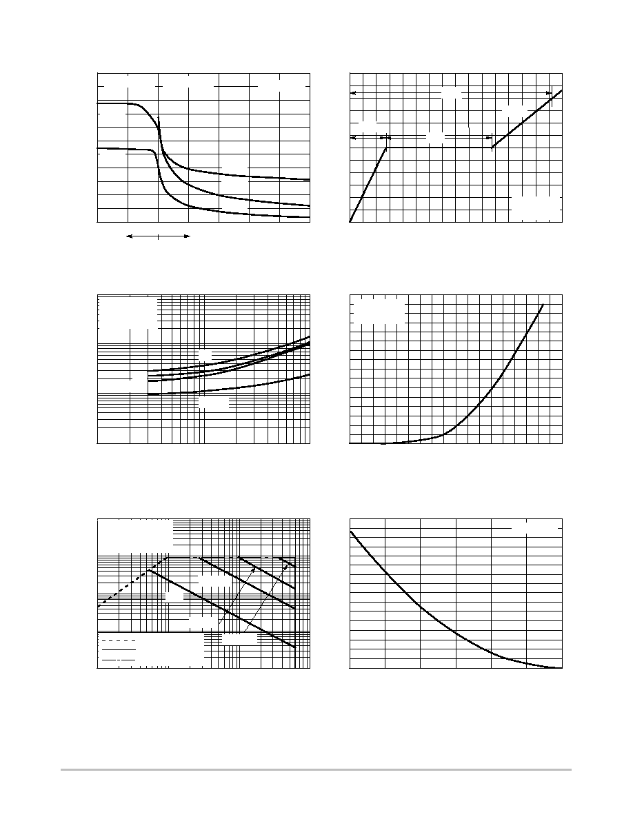
Figure 1. On-Region Characteristics
Figure 2. Transfer Characteristics
Figure 3. On-Resistance vs. Gate-to-Source
Voltage
Figure 4. On-Resistance vs. Drain Current and
Gate Voltage
Figure 5. On-Resistance Variation with
Temperature
Figure 6. Drain-to-Source Leakage Current
vs. Voltage
V
GS,
GATE-TO-SOURCE VOLTAGE (VOLTS)
I
D,
DRAIN CURRENT (AMPS)
T
J
= 25
∞
C
T
J
= 100
∞
C
T
J
= -55
∞
C
0
0.16
0.14
0.12
0.1
0.08
0.02
1
4
6
I
D,
DRAIN CURRENT (AMPS)
R
DS(on),
DRAIN-T
O-SOURCE RESIST
ANCE (
W
)
I
D,
DRAIN CURRENT (AMPS)
R
DS(on),
DRAIN-T
O-SOURCE RESIST
ANCE (
W
)
V
GS
= 10 V
2
1.8
1.6
1.4
T
J
, JUNCTION TEMPERATURE (
∞
C)
R
DS(on),
DRAIN-T
O-SOURCE RESIST
ANCE (NORMALIZED)
-50
50
25
0
-25
75
125
100
I
D
= 1.5 A
V
GS
= 5 V
0.8
0.6
150
1
10
1000
10000
V
DS,
DRAIN-TO-SOURCE VOLTAGE (VOLTS)
I
DSS
, LEAKAGE (nA)
0
40
60
30
20
10
50
100
5
3
0
2
5
3
2
1
V
DS,
DRAIN-TO-SOURCE VOLTAGE (VOLTS)
I
D,
DRAIN CURRENT (AMPS)
0
0.5
6
V
GS
= 5 V
V
GS
= 2.5 V
V
GS
= 6 V
V
GS
= 10 V
V
GS
= 3 V
4
1
1.5
2.5
1
5
2
4
1.5
2.5
3
3.5
4.5
0.06
0.04
2
V
GS,
GATE-TO-SOURCE VOLTAGE (VOLTS)
1.2
3
2
5
0
6
4
1
3
0
0.16
0.14
0.12
0.1
0.08
0.02
1
4
6
5
3
0.06
0.04
2
1
175
V
GS
= 2.8 V
V
GS
= 3.2 V
V
GS
= 3.4 V
V
GS
= 3.5 V
V
GS
= 4.5 V
T
J
= 150
∞
C
T
J
= 100
∞
C
T
J
= 25
∞
C
T
J
= 100
∞
C
T
J
= -55
∞
C
T
J
= 25
∞
C
T
J
= 100
∞
C
T
J
= -55
∞
C
V
DS
> = 10 V
V
GS
= 0 V
NTF3055L108
http://onsemi.com
4
10
10
15
5
0
20
5
25
R
DS(on)
LIMIT
V
GS
100
10
1
0.01
1000
10
1
6
5
4
3
2
1
0
60
20
10
0
3.2
2.8
2.4
2
0
1000
800
600
GATE-TO-SOURCE OR DRAIN-TO-SOURCE VOLTAGE
(VOLTS)
C, CAP
ACIT
ANCE (pF)
400
200
Q
g
, TOTAL GATE CHARGE (nC)
Figure 7. Capacitance Variation
Figure 8. Gate-to-Source and
Drain-to-Source Voltage vs. Total Charge
V
GS
, GA
TE-T
O-SOURCE VOL
T
AGE (VOL
TS
)
Figure 9. Resistive Switching Time Variation
vs. Gate Resistance
R
G
, GATE RESISTANCE (
W
)
Figure 10. Diode Forward Voltage vs. Current
V
SD
, SOURCE-TO-DRAIN VOLTAGE (VOLTS)
I
S
, SOURCE CURRENT (AMPS)
t, TIME (ns)
Figure 11. Maximum Rated Forward Biased
Safe Operating Area
V
DS
, DRAIN-TO-SOURCE VOLTAGE (VOLTS)
Figure 12. Maximum Avalanche Energy vs.
Starting Junction Temperature
T
J
, STARTING JUNCTION TEMPERATURE (
∞
C)
I
D
, DRAIN CURRENT (AMPS)
E
AS
, SINGLE PULSE DRAIN-T
O-SOURCE
A
V
ALANCHE ENERGY (mJ)
0
5
7
6
4
2
8
1
10
100
0.54
0.7
0.82
0.66
0.62
0.86
0.58
0.1
10
100
1
25
125
150
100
75
175
50
I
D
= 3 A
T
J
= 25
∞
C
V
GS
V
GS
= 0 V
V
DS
= 0 V
T
J
= 25
∞
C
C
rss
C
iss
C
oss
C
rss
1.6
1.2
0.74 0.78
C
iss
V
GS
= 15 V
SINGLE PULSE
T
C
= 25
∞
C
V
DS
= 30 V
I
D
= 3 A
V
GS
= 5 V
V
GS
= 0 V
T
J
= 25
∞
C
I
D
= 7 A
1 ms
100
m
s
10 ms
dc
t
r
t
d(off)
t
d(on)
V
DS
0.9
0.1
30
40
50
Q
2
Q
1
Q
T
70
80
0
3
1
100
0.8
0.4
t
f
THERMAL LIMIT
PACKAGE LIMIT
NTF3055L108
http://onsemi.com
5
10
1
0.001
100
10
1
0.1
0.001
1000
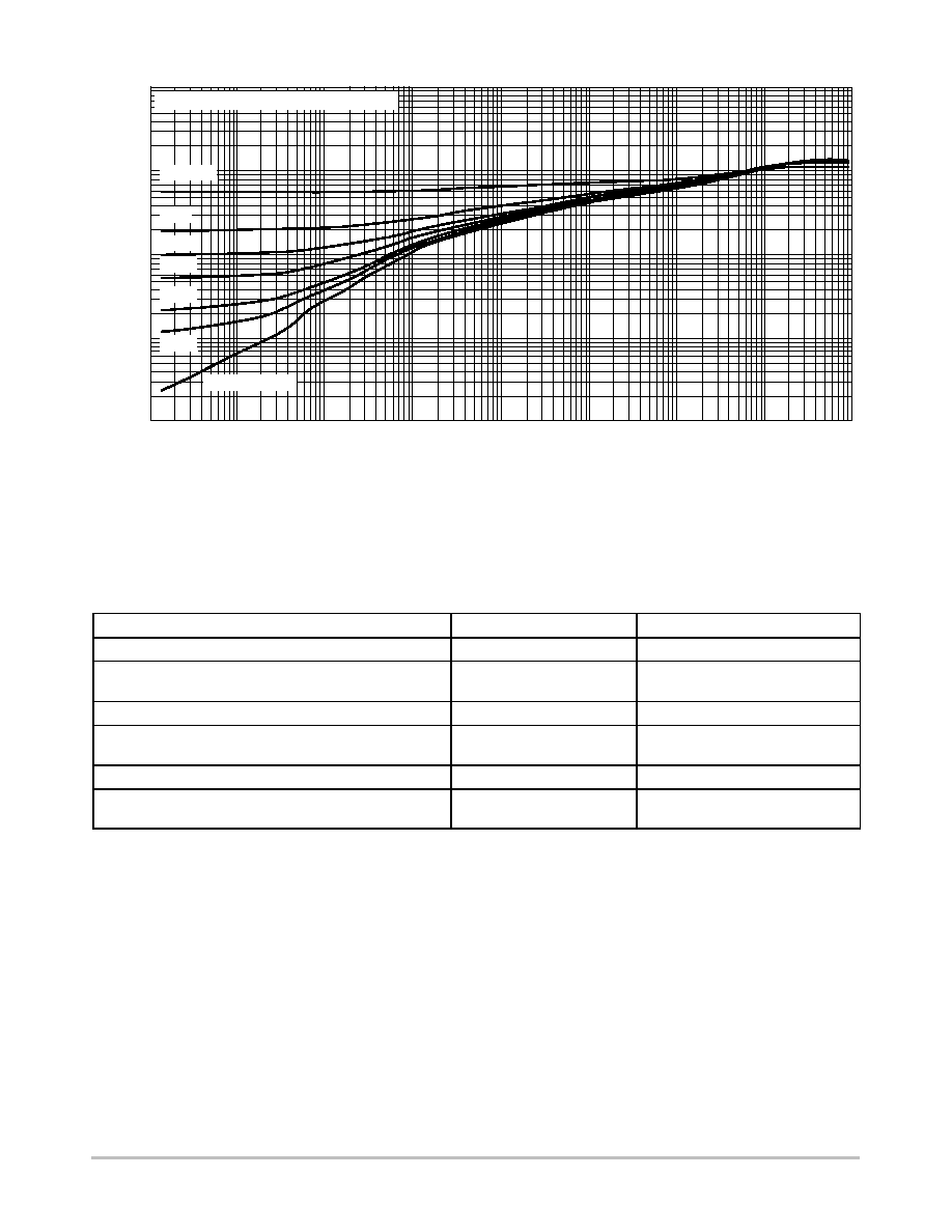
r(t), EFFECTIVE TRANSIENT THERMAL RESPONSE
RESIST
ANCE (NORMALIZED)
t, TIME (s)
1 x 1 inch 1 oz. Cu Pad (3 x 3 inch FR4)
Figure 13. Thermal Response
0.1
0.01
0.01
0.0001
0.00001
D = 0.5
0.2
0.1
0.05
0.02
0.01
Single Pulse
ORDERING INFORMATION
Device
Package
Shipping
NTF3055L108T1
SOT-223 (TO-261)
1000 / Tape & Reel
NTF3055L108T1G
SOT-223 (TO-261)
(Pb-Free)
1000 / Tape & Reel
NTF3055L108T3
SOT-223 (TO-261)
4000 / Tape & Reel
NTF3055L108T3G
SOT-223 (TO-261)
(Pb-Free)
4000 / Tape & Reel
NTF3055L108T3LF
SOT-223 (TO-261)
4000 / Tape & Reel
NTF3055L108T3LFG
SOT-223 (TO-261)
(Pb-Free)
4000 / Tape & Reel
For information on tape and reel specifications, including part orientation and tape sizes, please refer to our Tape and Reel Packaging
Specifications Brochure, BRD8011/D.