©
Semiconductor Components Industries, LLC, 2005
September, 2005 - Rev. 4
1
Publication Order Number:
NUD3048/D
NUD3048
FET Switch
100 V, 800 m
W
, N-Channel, TSOP-6
The NUD3048 provides a single device solution for a number of
applications requiring a low power, high voltage, FET switch. The
package includes a gate resistor and gate to source zener clamp. This
switch can accommodate a wide range of input voltages, making it
compatible with most current logic levels. Its 100 V rating makes it
compatible with 48 V telecom applications.
Features
∑
100 V Rating On Gate 2
∑
Integrated 100 k R
g
Option
∑
Integrated ESD Diode Protection
∑
Low Threshold Voltage
∑
Pb-Free Package is Available
Typical Applications
∑
FET Switch
∑
Inverter
∑
Level Shifter
∑
Inrush Limiter
∑
Relay Driver
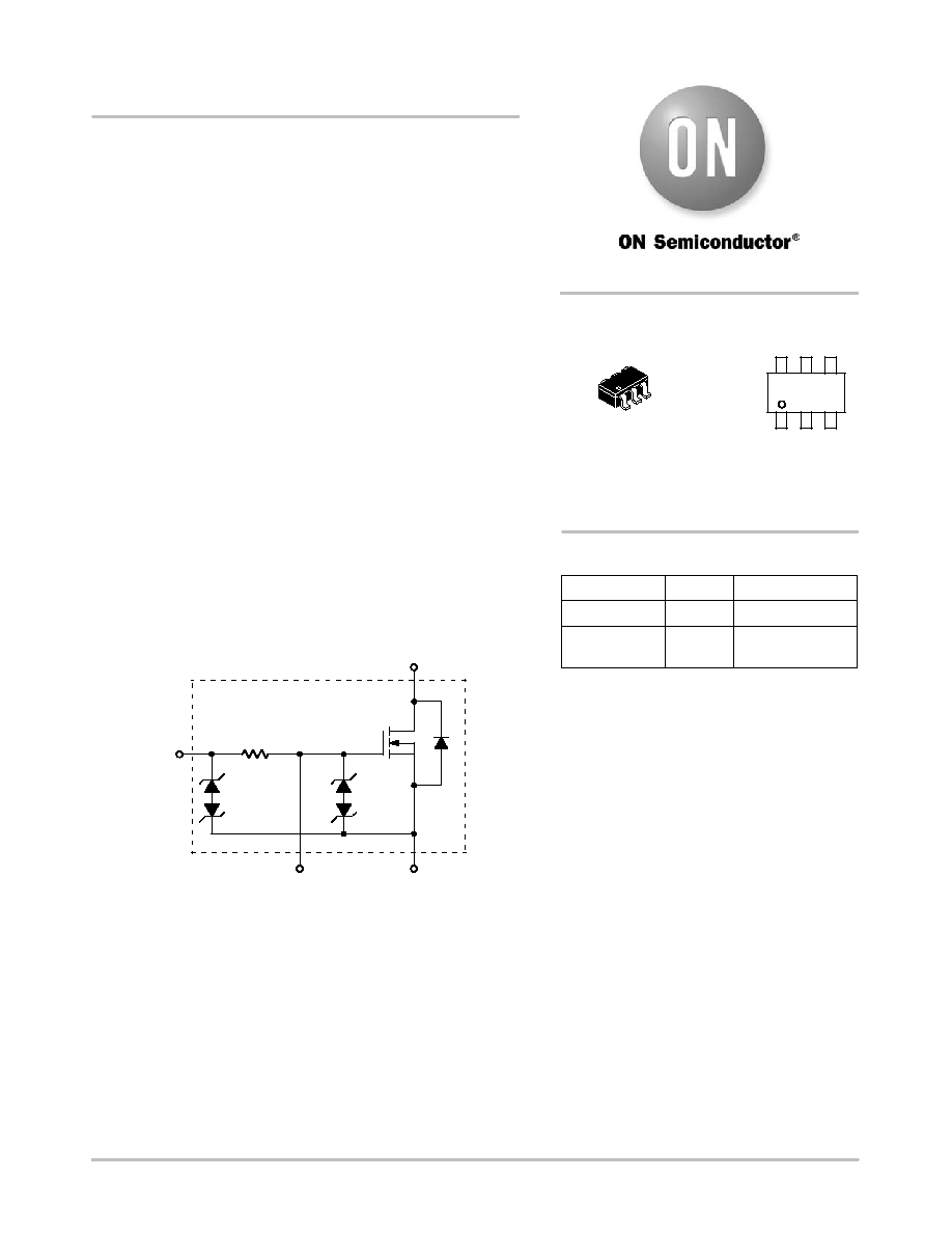
Figure 1. Block Diagram
Gate 2
6
100 k
W
1
3
Gate 1
Source
Drain
2, 4, 5
TSOP-6
CASE 318G
STYLE 9
http://onsemi.com
MARKING
DIAGRAM
1
6
JW7 M
G
G
JW7 = Specific Device Code
M
= Month Code
G
= Pb-Free Package
(Note: Microdot may be in either location)
Device
Package
Shipping
ORDERING INFORMATION
TSOP-6
3000 / Tape & Reel
NUD3048MT1
1
6
http://onsemi.com
TSOP-6
(Pb-Free)
3000 / Tape & Reel
NUD3048MT1G
For information on tape and reel specifications,
including part orientation and tape sizes, please
refer to our Tape and Reel Packaging Specifications
Brochure, BRD8011/D.

NUD3048
http://onsemi.com
2
MAXIMUM RATINGS
Symbol
Rating
Value
Unit
V
DSS
Drain to Source Voltage ≠ Continuous
100
V
V
G1SS
Gate to Source Voltage ≠ Continuous @ 1.0 mA
15
V
I
D
Drain Current ≠ Continuous (T
A
=25
_
C)
(Note 1)
(Note 2)
0.7
1.2
A
P
D
Power Dissipation (T
A
=25
_
C) (Note 1)
(Note 2)
0.66
1.56
W
V
G2SS
Gate Resistor to Source Voltage ≠ Continuous
100
V
T
Jmax
Maximum Junction Temperature
150
∞
C
R
q
JA
Thermal Impedance (Junction-to-Ambient) (Note 1)
Thermal Impedance (Junction-to-Ambient) (Note 2)
190
80
∞
C/W
ESD
Human Body Model (HBM) Class 2
Machine Model Class A
According to EIA/JESD22/A114 Specification
2000
100
V
V
Maximum ratings are those values beyond which device damage can occur. Maximum ratings applied to the device are individual stress limit values
(not normal operating conditions) and are not valid simultaneously. If these limits are exceeded, device functional operation is not implied, damage
may occur and reliability may be affected.
ELECTRICAL CHARACTERISTICS
(T
J
=25
_
C unless otherwise noted.)
Characteristic
Symbol
Min
Typ
Max
Unit
OFF CHARACTERISTICS
Drain to Source Leakage Current (V
DS
= 80 V, V
GS
= 0 V)
I
DSS
-
20
100
m
A
Gate Body Leakage Current
(V
GS
=10 V, V
DS
= 0 V)
(V
GS
= 10 V, V
DS
= 0 V, T
J
= 125
∞
C)
I
GSS
I
GSS
-
-
3.0
6.0
10
20
m
A
ON CHARACTERISTICS
Gate Threshold Voltage (I
D
= 1.0 mA)
V
GS
1.3
1.7
2.0
V
Drain to Source Resistance (V
GS
= 4.5 V, I
D
= 100 mA)
R
DS(on)
-
0.65
0.82
W
Drain to Source Resistance (V
GS
= 10 V, I
D
= 100 mA)
R
DS(on)
-
0.6
0.72
W
DYNAMIC CHARACTERISTICS
Input Capacitance (V
DS
= 5.0 V, V
GS
= 0 V, f = 10 kHz)
C
iss
-
135
-
pF
Output Capacitance (V
DS
= 5.0 V, V
GS
= 0 V, f = 10 kHz)
C
oss
-
75
-
pF
Transfer Capacitance (V
DS
= 5.0 V, V
GS
= 0 V, f = 10 kHz)
C
rss
-
26
-
pF
GATE BIAS CHARACTERISTICS
Gate Resistor
R
G
75
100
125
k
W
Gate Zener Breakdown Voltage (I
Z
= 1.0 mA) (Note 3)
Gate Zener Breakdown Voltage (I
Z
= 3.0 mA) (Note 4)
V
Z
15
100
17
115
-
-
V
1. Min pad, 1 oz. Cu.
2. 1 inch pad, 1 oz Cu.
3. Measured from gate 1 to source.
4. Measured from gate 2 to source.

NUD3048
http://onsemi.com
3
Figure 2. V
DS(on)
Variation with I
DS
and
Gate Voltage
0
0.1
0.2
0.3
0.4
0.5
0
0.1
0.2
0.3
0.4
0.5
I
DS
(A)
V
D
S
(on)
(V)
V
GS
= 2.0 V
V
GS
= 3.0 V
V
GS
= 5.0 V
V
GS
= 7.0 V
V
GS
= 10 V
0.55
0.60
0.65
0.70
0
0.05 0.1
0.15
0.2 0.25
0.3 0.35
0.4 0.45
Figure 3. On Resistance Variation with
Drain Current and Gate Voltage
R
D
S
(on)
(
W
)
I
D
(A)
0.0
0.2
0.4
0.6
0.8
1.0
1.2
1.4
1.6
1.8
2.0
-10
-8
-6
-4
-2
0
2
4
6
8
10
Figure 4. Variation of R
DS(on)
with
Temperature and Gate Voltage at I
D
= 100 mA
I
GS
(
m
A)
V
GS
(V)
V
GS
= 4.5 V
V
GS
= 10 V
V
GS
= 4.5 V
0
0.2
0.4
0.6
0.8
1
1.2
1.4
-50
0
50
100
150
Figure 5. Gate Leakage Current Variation
with Gate Voltage
R
DS(on)
VARIATION WITH TEMPERATURE
R
D
S
(on)
V
GS
= 4.5 V
V
GS
= 10 V
V
GS
= 4.5 V
0.5
6.00E-05
6.20E-05
6.40E-05
6.60E-05
6.80E-05
7.00E-05
7.20E-05
7.40E-05
-40.0 -20.0
0.0
20.0
40.0
60.0
80.0
100.0 120.0
Figure 6. Variation of Leakage Current I
DSS
(A)
with V
GS
= 0 V and V
DS
= 100 V
LEAKAGE
CURRENT I
DS
S
JUNCTION TEMPERATURE
I
DSS

NUD3048
http://onsemi.com
4
PACKAGE DIMENSIONS
TSOP-6
CASE 318G-02
ISSUE P
STYLE 9:
PIN 1. LOW VOLTAGE GATE
2. DRAIN
3. SOURCE
4. DRAIN
5. DRAIN
6. HIGH VOLTAGE GATE
2
3
4
5
6
D
1
e
b
E
A1
A
0.05 (0.002)
NOTES:
1. DIMENSIONING AND TOLERANCING PER
ANSI Y14.5M, 1982.
2. CONTROLLING DIMENSION: MILLIMETER.
3. MAXIMUM LEAD THICKNESS INCLUDES LEAD
FINISH THICKNESS. MINIMUM LEAD
THICKNESS IS THE MINIMUM THICKNESS OF
BASE MATERIAL.
4. DIMENSIONS A AND B DO NOT INCLUDE
MOLD FLASH, PROTRUSIONS, OR GATE
BURRS.
c
L
H
E
DIM
A
MIN
NOM
MAX
MIN
MILLIMETERS
0.90
1.00
1.10
0.035
INCHES
A1
0.01
0.06
0.10
0.001
b
0.25
0.38
0.50
0.010
c
0.10
0.18
0.26
0.004
D
2.90
3.00
3.10
0.114
E
1.30
1.50
1.70
0.051
e
0.85
0.95
1.05
0.034
L
0.20
0.40
0.60
0.008
0.039
0.043
0.002
0.004
0.014
0.020
0.007
0.010
0.118
0.122
0.059
0.067
0.037
0.041
0.016
0.024
NOM
MAX
2.50
2.75
3.00
0.099
0.108
0.118
H
E
-
-
0
∞
1
0
∞
0
∞
1
0
∞
q
q
0.95
0.037
1.9
0.075
0.95
0.037
mm
inches
SCALE 10:1
1.0
0.039
2.4
0.094
0.7
0.028
*For additional information on our Pb-Free strategy and soldering
details, please download the ON Semiconductor Soldering and
Mounting Techniques Reference Manual, SOLDERRM/D.
SOLDERING FOOTPRINT*
ON Semiconductor and are registered trademarks of Semiconductor Components Industries, LLC (SCILLC). SCILLC reserves the right to make changes without further notice
to any products herein. SCILLC makes no warranty, representation or guarantee regarding the suitability of its products for any particular purpose, nor does SCILLC assume any
liability arising out of the application or use of any product or circuit, and specifically disclaims any and all liability, including without limitation special, consequential or incidental
damages. "Typical" parameters which may be provided in SCILLC data sheets and/or specifications can and do vary in different applications and actual performance may vary over
time. All operating parameters, including "Typicals" must be validated for each customer application by customer's technical experts. SCILLC does not convey any license under
its patent rights nor the rights of others. SCILLC products are not designed, intended, or authorized for use as components in systems intended for surgical implant into the body,
or other applications intended to support or sustain life, or for any other application in which the failure of the SCILLC product could create a situation where personal injury or death
may occur. Should Buyer purchase or use SCILLC products for any such unintended or unauthorized application, Buyer shall indemnify and hold SCILLC and its officers, employees,
subsidiaries, affiliates, and distributors harmless against all claims, costs, damages, and expenses, and reasonable attorney fees arising out of, directly or indirectly, any claim of
personal injury or death associated with such unintended or unauthorized use, even if such claim alleges that SCILLC was negligent regarding the design or manufacture of the part.
SCILLC is an Equal Opportunity/Affirmative Action Employer. This literature is subject to all applicable copyright laws and is not for resale in any manner.
PUBLICATION ORDERING INFORMATION
N. American Technical Support: 800-282-9855 Toll Free
USA/Canada
Japan: ON Semiconductor, Japan Customer Focus Center
2-9-1 Kamimeguro, Meguro-ku, Tokyo, Japan 153-0051
Phone: 81-3-5773-3850
NUD3048/D
LITERATURE FULFILLMENT:
Literature Distribution Center for ON Semiconductor
P.O. Box 61312, Phoenix, Arizona 85082-1312 USA
Phone: 480-829-7710 or 800-344-3860 Toll Free USA/Canada
Fax: 480-829-7709 or 800-344-3867 Toll Free USA/Canada
Email: orderlit@onsemi.com
ON Semiconductor Website: http://onsemi.com
Order Literature: http://www.onsemi.com/litorder
For additional information, please contact your
local Sales Representative.