 | –≠–ª–µ–∫—Ç—Ä–æ–Ω–Ω—ã–π –∫–æ–º–ø–æ–Ω–µ–Ω—Ç: NUD3124D | –°–∫–∞—á–∞—Ç—å:  PDF PDF  ZIP ZIP |

©
Semiconductor Components Industries, LLC, 2004
June, 2004 - Rev. 8
1
Publication Order Number:
NUD3124/D
NUD3124
Automotive Inductive Load
Driver
This MicroIntegration
t part provides a single component solution
to switch inductive loads such as relays, solenoids, and small DC
motors without the need of a free-wheeling diode. It accepts logic
level inputs, thus allowing it to be driven by a large variety of devices
including logic gates, inverters, and microcontrollers.
Features
∑
Provides Robust Interface between D.C. Relay Coils and Sensitive
Logic
∑
Capable of Driving Relay Coils Rated up to 150 mA at 12 Volts
∑
Replaces 3 or 4 Discrete Components for Lower Cost
∑
Internal Zener Eliminates Need for Free-Wheeling Diode
∑
Meets Load Dump and other Automotive Specs
∑
Pb-Free Package is Available
Typical Applications
∑
Automotive and Industrial Environment
∑
Drives Window, Latch, Door, and Antenna Relays
Benefits
∑
Reduced PCB Space
∑
Standardized Driver for Wide Range of Relays
∑
Simplifies Circuit Design and PCB Layout
∑
Compliance with Automotive Specifications
Gate (1)
10 k
100 K
Drain (3)
Source (2)
INTERNAL CIRCUIT DIAGRAMS
Gate (2)
10 k
100 K
Drain (6)
Source (1)
Gate (5)
Drain (3)
Source (4)
10 k
100 K
CASE 318
CASE 318F
http://onsemi.com
Device
Package
Shipping
ORDERING INFORMATION
NUD3124LT1
SOT-23
3000/Tape & Reel
MARKING DIAGRAMS
1
2
3
SOT-23
CASE 318
STYLE 21
JW6 D
JW6
= Specific Device Code
D
= Date Code
JW6 D
SC-74
CASE 318F
STYLE 7
1
6
JW6
= Specific Device Code
D
= Date Code
NUD3124LT1G
SOT-23
(Pb-Free)
3000/Tape & Reel
For information on tape and reel specifications,
including part orientation and tape sizes, please
refer to our Tape and Reel Packaging Specification
Brochure, BRD8011/D.
NUD3124DMT1
SC-74
3000/Tape & Reel
NUD3124
http://onsemi.com
2
MAXIMUM RATINGS
(T
J
= 25
∞
C unless otherwise specified)
Symbol
Rating
Value
Unit
V
DSS
Drain-to-Source Voltage ≠ Continuous
(T
J
= 125
∞
C)
28
V
V
GSS
Gate-to-Source Voltage ≠ Continuous
(T
J
= 125
∞
C)
12
V
I
D
Drain Current ≠ Continuous
(T
J
= 125
∞
C)
150
mA
E
Z
Single Pulse Drain-to-Source Avalanche Energy
(For Relay's Coils/Inductive Loads of 80
W
or Higher)
(T
J
Initial
= 85
∞
C)
250
mJ
P
PK
Peak Power Dissipation, Drain-to-Source (Notes 1 and 2)
(T
J
Initial
= 85
∞
C)
20
W
E
LD1
Load Dump Suppressed Pulse, Drain-to-Source (Notes 3 and 4)
(Suppressed Waveform: V
s
= 45 V, R
SOURCE
= 0.5
W
, T = 200 ms)
(For Relay's Coils/Inductive Loads of 80
W
or Higher)
(T
J
Initial
= 85
∞
C)
80
V
E
LD2
Inductive Switching Transient 1, Drain-to-Source
(Waveform: R
SOURCE
= 10
W
, T = 2.0 ms)
(For Relay's Coils/Inductive Loads of 80
W
or Higher)
(T
J
Initial
= 85
∞
C)
100
V
E
LD3
Inductive Switching Transient 2, Drain-to-Source
(Waveform: R
SOURCE
= 4.0
W
, T = 50
m
s)
(For Relay's Coils/Inductive Loads of 80
W
or Higher)
(T
J
Initial
= 85
∞
C)
300
V
Rev-Bat
Reverse Battery, 10 Minutes (Drain-to-Source)
(For Relay's Coils/Inductive Loads of 80
W
or more)
-14
V
Dual-Volt
Dual Voltage Jump Start, 10 Minutes (Drain-to-Source)
28
V
ESD
Human Body Model (HBM)
According to EIA/JESD22/A114 Specification
2,000
V
1. Nonrepetitive current square pulse 1.0 ms duration.
2. For different square pulse durations, see Figure 2.
3. Nonrepetitive load dump suppressed pulse per Figure 3.
4. For relay's coils/inductive loads higher than 80
W
, see Figure 4.
THERMAL CHARACTERISTICS
Symbol
Rating
Value
Unit
T
A
Operating Ambient Temperature
-40 to 125
∞
C
T
J
Maximum Junction Temperature
150
∞
C
T
STG
Storage Temperature Range
-65 to 150
∞
C
P
D
Total Power Dissipation (Note 5)
SOT-23
Derating above 25
∞
C
225
1.8
mW
mW/
∞
C
P
D
Total Power Dissipation (Note 5)
SC-74
Derating above 25
∞
C
380
3.0
mW
mW/
∞
C
R
q
JA
Thermal Resistance Junction≠to≠Ambient (Note 5)
SOT-23
SC-74
556
329
∞
C/W
5. Mounted onto minimum pad board.
NUD3124
http://onsemi.com
3
ELECTRICAL CHARACTERISTICS
(T
J
= 25
∞
C unless otherwise specified)
Characteristic
Symbol
Min
Typ
Max
Unit
OFF CHARACTERISTICS
Drain to Source Sustaining Voltage
(I
D
= 10 mA)
V
BRDSS
28
34
38
V
Drain to Source Leakage Current
(V
DS
= 12 V, V
GS
= 0 V)
(V
DS
= 12 V, V
GS
= 0 V, T
J
= 125
∞
C)
(V
DS
= 28 V, V
GS
= 0 V)
(V
DS
= 28 V, V
GS
= 0 V, T
J
= 125
∞
C)
I
DSS
-
-
-
-
-
-
-
-
0.5
1.0
50
80
m
A
Gate Body Leakage Current
(V
GS
= 3.0 V, V
DS
= 0 V)
(V
GS
= 3.0 V, V
DS
= 0 V, T
J
= 125
∞
C)
(V
GS
= 5.0 V, V
DS
= 0 V)
(V
GS
= 5.0 V, V
DS
= 0 V, T
J
= 125
∞
C)
I
GSS
-
-
-
-
-
-
-
-
60
80
90
110
m
A
ON CHARACTERISTICS
Gate Threshold Voltage
(V
GS
= V
DS
, I
D
= 1.0 mA)
(V
GS
= V
DS
, I
D
= 1.0 mA, T
J
= 125
∞
C)
V
GS(th)
1.3
1.3
1.8
-
2.0
2.0
V
Drain to Source On-Resistance
(I
D
= 150 mA, V
GS
= 3.0 V)
(I
D
= 150 mA, V
GS
= 3.0 V, T
J
= 125
∞
C)
(I
D
= 150 mA, V
GS
= 5.0 V)
(I
D
= 150 mA, V
GS
= 5.0 V, T
J
= 125
∞
C)
R
DS(on)
-
-
-
-
-
-
-
-
1.4
1.7
0.8
1.1
W
Output Continuous Current
(V
DS
= 0.25 V, V
GS
= 3.0 V)
(V
DS
= 0.25 V, V
GS
= 3.0 V, T
J
= 125
∞
C)
I
DS(on)
150
140
200
-
-
-
mA
Forward Transconductance
(V
DS
= 12 V, I
D
= 150 mA)
g
FS
-
500
-
mmho
DYNAMIC CHARACTERISTICS
Input Capacitance
(V
DS
= 12 V, V
GS
= 0 V, f = 10 kHz)
Ciss
-
32
-
pf
Output Capacitance
(V
DS
= 12 V, V
GS
= 0 V, f = 10 kHz)
Coss
-
21
-
pf
Transfer Capacitance
(V
DS
= 12 V, V
GS
= 0 V, f = 10 kHz)
Crss
-
8.0
-
pf
SWITCHING CHARACTERISTICS
Propagation Delay Times:
High to Low Propagation Delay; Figure 1, (V
DS
= 12 V, V
GS
= 3.0 V)
Low to High Propagation Delay; Figure 1, (V
DS
= 12 V, V
GS
= 3.0 V)
High to Low Propagation Delay; Figure 1, (V
DS
= 12 V, V
GS
= 5.0 V)
Low to High Propagation Delay; Figure 1, (V
DS
= 12 V, V
GS
= 5.0 V)
t
PHL
t
PLH
t
PHL
t
PLH
-
-
-
-
890
912
324
1280
-
-
-
-
ns
Transition Times:
Fall Time; Figure 1, (V
DS
= 12 V, V
GS
= 3.0 V)
Rise Time; Figure 1, (V
DS
= 12 V, V
GS
= 3.0 V)
Fall Time; Figure 1, (V
DS
= 12 V, V
GS
= 5.0 V)
Rise Time; Figure 1, (V
DS
= 12 V, V
GS
= 5.0 V)
t
f
t
r
t
f
t
r
-
-
-
-
2086
708
556
725
-
-
-
-
ns
NUD3124
http://onsemi.com
4
TYPICAL PERFORMANCE CURVES
(T
J
= 25
∞
C unless otherwise noted)
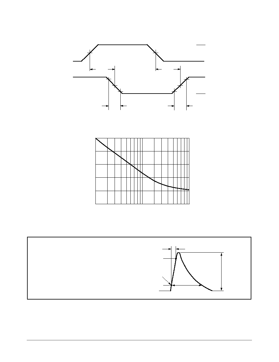
Figure 1. Switching Waveforms
Load Dump Pulse Not Suppressed:
V
R
= 13.5 V Nominal
±
10%
V
S
= 60 V Nominal
±
10%
T = 300 ms Nominal
±
10%
T
R
= 1 - 10 ms
±
10%
Load Dump Pulse Suppressed:
NOTE: Max. Voltage DUT is exposed to is
NOTE:
approximately 45 V.
V
S
= 30 V
±
20%
T = 150 ms
±
20%
Figure 2. Maximum Non-repetitive Surge
Power versus Pulse Width
P
W
, PULSE WIDTH (ms)
100
10
1
0
5
10
15
20
25
P
pk
, PEAK SURGE POWER (W)
Figure 3. Load Dump Waveform Definition
VS
T
R
90%
10%
T
V
R
, I
R
10% of Peak;
Reference = V
R
, I
R
V
out
V
in
0 V
V
OH
V
IH
t
r
t
f
t
PLH
t
PHL
50%
90%
50%
10%
V
OL

NUD3124
http://onsemi.com
5
Figure 4. Load Dump Capability versus
Relay's Coil dc Resistance
RELAY'S COIL (
W
)
350
260
230
200
170
140
110
80
40
60
80
100
120
140
Figure 5. Drain-to-Source Leakage versus
Junction Temperature
Figure 6. Gate-to-Source Leakage versus
Junction Temperature
T
J
, JUNCTION TEMPERATURE (
∞
C)
T
J
, JUNCTION TEMPERATURE (
∞
C)
75
50
25
0
-25
-50
0
2
4
6
8
10
14
100
50
25
0
-25
-50
20
30
40
50
60
70
80
Figure 7. Breakdown Voltage versus Junction
Temperature
T
J
, JUNCTION TEMPERATURE (
∞
C)
125
50
0
-25
-50
33.6
33.8
34.0
34.4
34.6
34.8
V
S
, LOAD DUMP (VOL
TS)
320
290
I
DSS
, DRAIN LEAKAGE (
m
A)
125
100
75
125
I
GS
S
GA
TE LEAKAGE (
m
A)
V
GS
= 5 V
V
GS
= 3 V
25
100
75
34.2
33.4
BV
DSS
BREAKDOWN VOL
T
AGE (V)
I
D
= 10 mA
Figure 8. Output Characteristics
V
DS
= 28 V
Figure 9. Transfer Function
V
DS
, DRAIN-TO-SOURCE VOLTAGE (V)
0.7
0.5
0.4
0.3
0.2
0.0
1E-10
1E-08
1E-06
1E-04
0.01
1
0.1
0.6
0.8
I
D
DRAIN CURRENT (A)
V
GS
= 5 V
V
GS
= 3 V
12
V
GS
= 2 V
V
GS
= 2.5 V
V
GS
= 1 V
V
GS
, GATE-TO-SOURCE VOLTAGE (V)
4.5
3.0
2.5
2.0
1.5
0.5
1E-07
1E-05
1E-06
1E-04
0.1
1
1.0
4.0
5.0
I
D
DRAIN CURRENT (A)
125
∞
C
3.5
0.001
0.01
85
∞
C
25
∞
C
-40
∞
C
V
DS
= 0.8 V