©
Semiconductor Components Industries, LLC, 2004
September, 2004 - Rev. P0
1
Publication Order Number:
NUP1105L/D
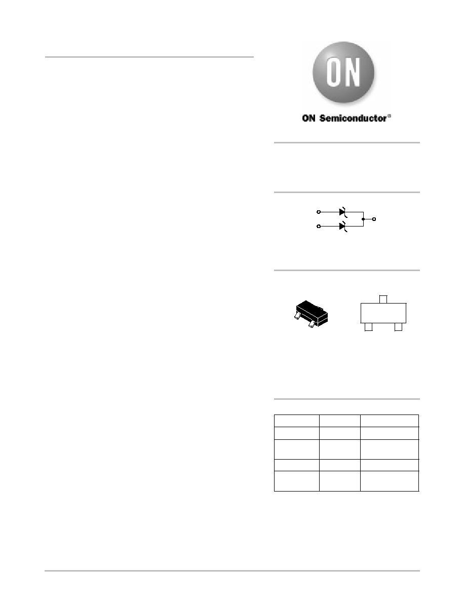
NUP1105L
Advance Information
Single Line CAN/LIN
Bus Protector
The NUP1105L has been designed to protect LIN and single line
CAN transceivers from ESD and other harmful transient voltage
events. This device provides bidirectional protection for the data line
with a single SOT-23 package, giving the system designer a low cost
option for improving system reliability and meeting stringent EMI
requirements.
Features
∑
SOT-23 Package Allows One Separate Bidirectional Configuration
∑
350 W Peak Power Dissipation per Line (8 x 20
msec Waveform)
∑
Low Reverse Leakage Current (< 100 nA)
∑
IEC Compatibility: - IEC 61000-4-2 (ESD): Level 4
- IEC 61000-4-4 (EFT): 40 A ≠ 5/50 ns
- IEC 61000-4-5 (Lighting) 8.0 A (8/20
ms)
∑
ISO 7637-1, Nonrepetitive EMI Surge Pulse TBD
∑
ISO 7637-3, Repetitive Electrical Fast Transient (EFT) TBD
EMI Surge Pulses
∑
Flammability Rating UL 94 V-0
∑
Pb-Free Packages are Available
Applications
∑
Automotive Electronics
LIN Bus
Single Line CAN
∑
Industrial Control Networks
Smart Distribution Systems (SDS
TM
)
DeviceNet
TM
This document contains information on a new product. Specifications and information
herein are subject to change without notice.
http://onsemi.com
Device
Package
Shipping
ORDERING INFORMATION
NUP1105LT1
SOT-23
3000/Tape & Reel
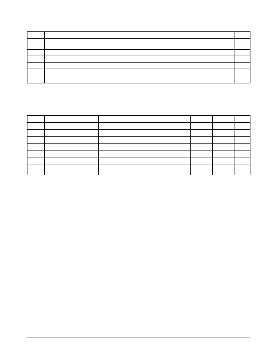
SOT-23
CASE 318
STYLE 27
MARKING
DIAGRAM
27D
= Device Code
M
= Date Code
SOT-23 BIDIRECTIONAL
VOLTAGE SUPPRESSOR
350 W PEAK POWER
For information on tape and reel specifications,
including part orientation and tape sizes, please
refer to our Tape and Reel Packaging Specification
Brochure, BRD8011/D.
1
27DM
1
3
2
PIN 1. ANODE
2. ANODE
3. CATHODE
NUP1105LT1G
SOT-23
(Pb-Free)
3000/Tape & Reel
NUP1105LT3
SOT-23
10000/Tape & Reel
NUP1105LT3G
SOT-23
(Pb-Free)
10000/Tape & Reel
NUP1105L
http://onsemi.com
2
MAXIMUM RATINGS
(T
J
= 25
∞
C, unless otherwise specified)
Symbol
Rating
Value
Unit
PPK
Peak Power Dissipation
8 x 20
m
s Double Exponential Waveform (Note 1)
350
W
T
J
Operating Junction Temperature Range
-40 to 125
∞
C
T
J
Storage Temperature Range
-55 to 150
∞
C
T
L
Lead Solder Temperature (10 s)
260
∞
C
ESD
Human Body model (HBM)
Machine Model (MM)
IEC 61000-4-2 Specification (Contact)
16
400
30
kV
V
kV
Maximum ratings are those values beyond which device damage can occur. Maximum ratings applied to the device are individual stress limit
values (not normal operating conditions) and are not valid simultaneously. If these limits are exceeded, device functional operation is not im-
plied, damage may occur and reliability may be affected.
1. Nonrepetitive current pulse per Figure 1.
ELECTRICAL CHARACTERISTICS
(T
J
= 25
∞
C, unless otherwise specified)
Symbol
Parameter
Test Conditions
Min
Typ
Max
Unit
V
RWM
Reverse Working Voltage
(Note 2)
24
V
V
BR
Breakdown Voltage
I
T
= 1 mA (Note 3)
25.7
28.4
V
I
R
Reverse Leakage Current
V
RWM
= 24 V
15
100
nA
V
C
Clamping Voltage
I
PP
= 5 A (8 x 20
m
s Waveform) (Note 4)
40
V
V
C
Clamping Voltage
I
PP
= 8 A (8 x 20
m
s Waveform) (Note 4)
44
V
I
PP
Maximum Peak Pulse Current
8 x 20
m
s Waveform (Note 4)
8.0
A
CJ
Capacitance
V
R
= 0 V, f = 1 MHz (Anode to GND)
V
R
= 0 V, f = 1 MHz (Anode to Anode)
60
30
pF
2. TVS devices are normally selected according to the working peak reverse voltage (V
RWM
), which should be equal or greater than the DC
or continuous peak operating voltage level.
3. V
BR
is measured at pulse test current I
T
.
4. Pulse waveform per Figure 1.
NUP1105L
http://onsemi.com
3
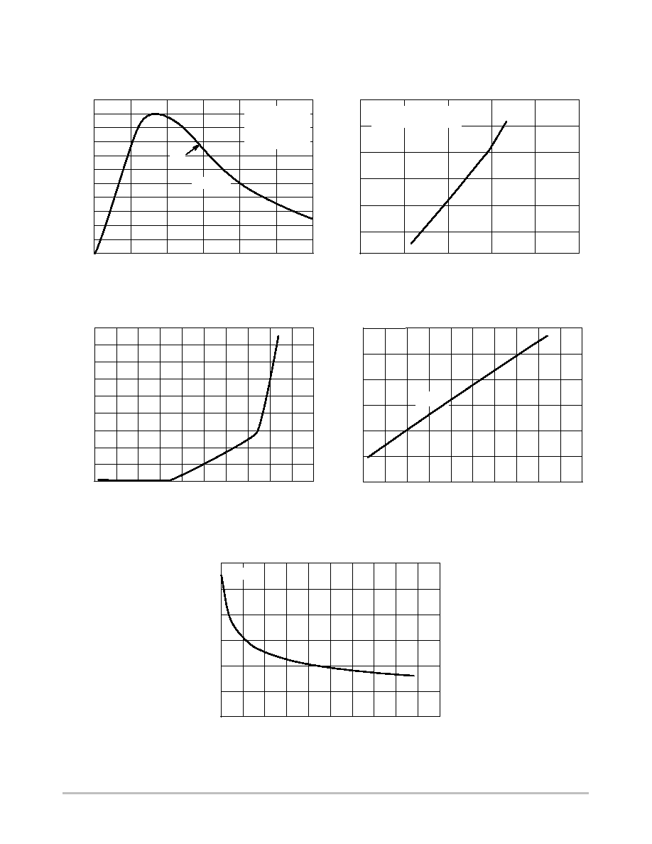
TYPICAL PERFORMANCE CURVES
(T
J
= 25
∞
C unless otherwise noted)
Figure 1. Pulse Waveform, 8
◊
20
m
s
110
90
80
70
60
50
40
30
20
10
0
0
5
15
25
t, TIME (
m
s)
% OF PEAK PULSE CURRENT
WAVEFORM
PARAMETERS
t
r
= 8
m
s
t
d
= 20
m
s
t
d
= I
PP
/2
30
Figure 2. Clamping Voltage vs Peak Pulse Current
12.0
10.0
8.0
6.0
4.0
2.0
0.0
25
40
V
C
, CLAMPING VOLTAGE (V)
I
PP
, PEAK PULSE CURRENT (A)
30
35
45
50
100
10
20
c-t
PULSE WAVEFORM
8 x 20
m
s per Figure 1
0
5
10
15
20
25
30
35
40
45
-60
-10
40
90
140
190
Figure 3. Typical Leakage vs. Temperature
TEMPERATURE (
∞
C)
I
R
, (A)
24
25
26
27
28
29
30
-60
-10
40
90
140
190
Figure 4. Typical V
Z
@ 1.0 mA vs. Temperature
V
Z
, (V)
TEMPERATURE (
∞
C)
V
Z
0
10
20
30
40
50
60
0
5
10
15
20
25
Figure 5. Capacitance vs. V
BIAS
V
BIAS
CAP
ACIT
ANCE (pF)
25
∞
C
NUP1105L
http://onsemi.com
4
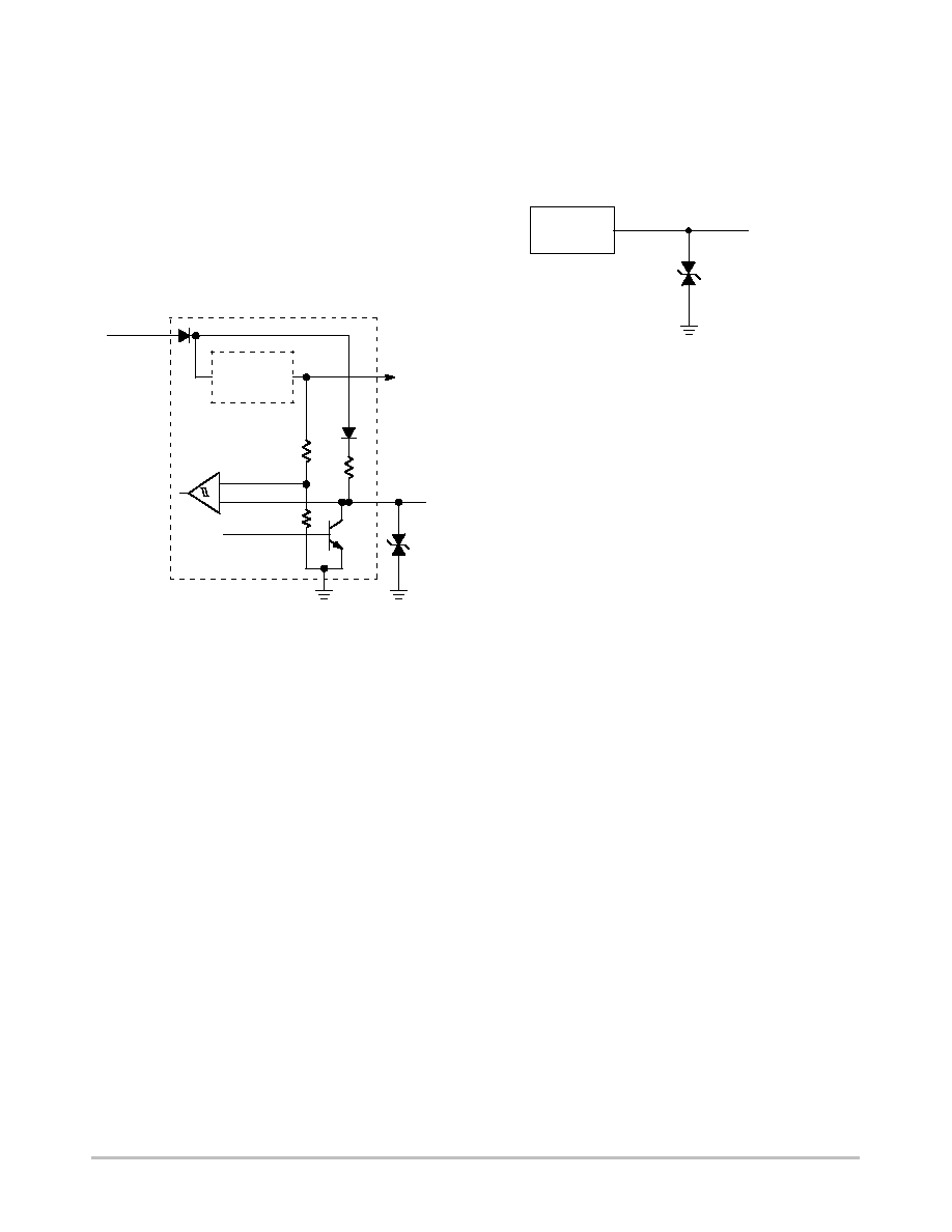
APPLICATIONS SECTION
The NUP1105L provides a transient voltage suppression
solution for the LIN data communication bus. The
NUP1105L is a dual bidirectional TVS device in a compact
SOT-23 package. This device is based on Zener technology
that optimizes the active area of a PN junction to provide
robust protection against transient EMI surge voltage and
ESD. The NUP1105L has been tested to EMI and ESD
levels that exceed the specifications of popular high speed
LIN networks.
Figure 6. LIN Transceiver
Voltage
Regulator
Transmitter
Receiver
LIN Bus
NUP1105L
V
OUT
= 5 V
V
Battery
=
8 to 18 V
LIN Transceiver
The NUP1105L device can be used to provide transcient
voltage suppression for a single data line CAN system.
Figure 7 provides an example of a single data line CAN
protection circuit.
Figure 7. High-Speed and Fault Tolerant CAN TVS
Protection Circuit
CAN
Transceiver
CAN_Data_Line
NUP1105L
NUP1105L
http://onsemi.com
5
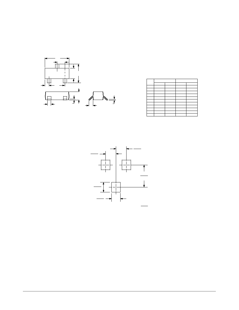
PACKAGE DIMENSIONS
mm
inches
SCALE 10:1
0.8
0.031
0.9
0.035
0.95
0.037
0.95
0.037
2.0
0.079
D
J
K
L
A
C
B S
H
G
V
3
1
2
DIM
A
MIN
MAX
MIN
MAX
MILLIMETERS
0.1102
0.1197
2.80
3.04
INCHES
B
0.0472
0.0551
1.20
1.40
C
0.0350
0.0440
0.89
1.11
D
0.0150
0.0200
0.37
0.50
G
0.0701
0.0807
1.78
2.04
H
0.0005
0.0040
0.013
0.100
J
0.0034
0.0070
0.085
0.177
K
0.0140
0.0285
0.35
0.69
L
0.0350
0.0401
0.89
1.02
S
0.0830
0.1039
2.10
2.64
V
0.0177
0.0236
0.45
0.60
SOT-23 (TO-236)
CASE 318-08
ISSUE AK
NOTES:
1. DIMENSIONING AND TOLERANCING PER ANSI
Y14.5M, 1982.
2. CONTROLLING DIMENSION: INCH.
3. MAXIMUM LEAD THICKNESS INCLUDES LEAD
FINISH THICKNESS. MINIMUM LEAD
THICKNESS IS THE MINIMUM THICKNESS OF
BASE MATERIAL.
4. 318-01 THRU -07 AND -09 OBSOLETE, NEW
STANDARD 318-08.
STYLE 27:
PIN 1. CATHODE
2. CATHODE
3. CATHODE
*For additional information on our Pb-Free strategy and soldering
details, please download the ON Semiconductor Soldering and
Mounting Techniques Reference Manual, SOLDERRM/D.
SOLDERING FOOTPRINT*

NUP1105L
http://onsemi.com
6
ON Semiconductor and are registered trademarks of Semiconductor Components Industries, LLC (SCILLC). SCILLC reserves the right to make changes without further notice
to any products herein. SCILLC makes no warranty, representation or guarantee regarding the suitability of its products for any particular purpose, nor does SCILLC assume any liability
arising out of the application or use of any product or circuit, and specifically disclaims any and all liability, including without limitation special, consequential or incidental damages.
"Typical" parameters which may be provided in SCILLC data sheets and/or specifications can and do vary in different applications and actual performance may vary over time. All
operating parameters, including "Typicals" must be validated for each customer application by customer's technical experts. SCILLC does not convey any license under its patent rights
nor the rights of others. SCILLC products are not designed, intended, or authorized for use as components in systems intended for surgical implant into the body, or other applications
intended to support or sustain life, or for any other application in which the failure of the SCILLC product could create a situation where personal injury or death may occur. Should
Buyer purchase or use SCILLC products for any such unintended or unauthorized application, Buyer shall indemnify and hold SCILLC and its officers, employees, subsidiaries, affiliates,
and distributors harmless against all claims, costs, damages, and expenses, and reasonable attorney fees arising out of, directly or indirectly, any claim of personal injury or death
associated with such unintended or unauthorized use, even if such claim alleges that SCILLC was negligent regarding the design or manufacture of the part. SCILLC is an Equal
Opportunity/Affirmative Action Employer. This literature is subject to all applicable copyright laws and is not for resale in any manner.
PUBLICATION ORDERING INFORMATION
N. American Technical Support: 800-282-9855 Toll Free
USA/Canada
Japan: ON Semiconductor, Japan Customer Focus Center
2-9-1 Kamimeguro, Meguro-ku, Tokyo, Japan 153-0051
Phone: 81-3-5773-3850
NUP1105L/D
SDS is a registered trademark of Honeywell International Inc.
DeviceNet is a trademark of Rockwell Automation.
LITERATURE FULFILLMENT:
Literature Distribution Center for ON Semiconductor
P.O. Box 61312, Phoenix, Arizona 85082-1312 USA
Phone: 480-829-7710 or 800-344-3860 Toll Free USA/Canada
Fax: 480-829-7709 or 800-344-3867 Toll Free USA/Canada
Email: orderlit@onsemi.com
ON Semiconductor Website: http://onsemi.com
Order Literature: http://www.onsemi.com/litorder
For additional information, please contact your
local Sales Representative.