©
Semiconductor Components Industries, LLC, 2004
September, 2004 - Rev. 1
1
Publication Order Number:
NUP2105L/D
NUP2105L
Dual Line CAN
Bus Protector
The NUP2105L has been designed to protect the CAN transceiver in
high-speed and fault tolerant networks from ESD and other harmful
transient voltage events. This device provides bidirectional protection
for each data line with a single compact SOT-23 package, giving the
system designer a low cost option for improving system reliability and
meeting stringent EMI requirements.
Features
∑
350 W Peak Power Dissipation per Line (8 x 20
msec Waveform)
∑
Low Reverse Leakage Current (< 100 nA)
∑
Low Capacitance High-Speed CAN Data Rates
∑
IEC Compatibility: - IEC 61000-4-2 (ESD): Level 4
- IEC 61000-4-4 (EFT): 40 A ≠ 5/50 ns
- IEC 61000-4-5 (Lighting) 8.0 A (8/20
ms)
∑
ISO 7637-1, Nonrepetitive EMI Surge Pulse 2, 9.5 A
(1 x 50
ms)
∑
ISO 7637-3, Repetitive Electrical Fast Transient (EFT)
EMI Surge Pulses, 50 A (5 x 50 ns)
∑
Flammability Rating UL 94 V-0
∑
Pb-Free Packages are Available
Applications
∑
Industrial Control Networks
Smart Distribution Systems (SDS
TM
)
DeviceNet
TM
∑
Automotive Networks
Low and High-Speed CAN
Fault Tolerant CAN
http://onsemi.com
Device
Package
Shipping
ORDERING INFORMATION
NUP2105LT1
SOT-23
3000/Tape & Reel
SOT-23
CASE 318
STYLE 27
PIN 1
PIN 3
PIN 2
MARKING
DIAGRAM
27D
= Device Code
M
= Date Code
SOT-23
DUAL BIDIRECTIONAL
VOLTAGE SUPPRESSOR
350 W PEAK POWER
For information on tape and reel specifications,
including part orientation and tape sizes, please
refer to our Tape and Reel Packaging Specification
Brochure, BRD8011/D.
1
27DM
CAN
Transceiver
CAN_H
CAN_L
NUP2105L
CAN Bus
NUP2105LT1G
SOT-23
(Pb-Free)
3000/Tape & Reel
NUP2105LT3
SOT-23
10000/Tape & Reel
NUP2105LT3G
SOT-23
(Pb-Free)
10000/Tape & Reel
NUP2105L
http://onsemi.com
2
MAXIMUM RATINGS
(T
J
= 25
∞
C, unless otherwise specified)
Symbol
Rating
Value
Unit
PPK
Peak Power Dissipation
8 x 20
m
s Double Exponential Waveform (Note 1)
350
W
T
J
Operating Junction Temperature Range
-40 to 125
∞
C
T
J
Storage Temperature Range
-55 to 150
∞
C
T
L
Lead Solder Temperature (10 s)
260
∞
C
ESD
Human Body model (HBM)
Machine Model (MM)
IEC 61000-4-2 Specification (Contact)
16
400
30
kV
V
kV
Maximum ratings are those values beyond which device damage can occur. Maximum ratings applied to the device are individual stress limit
values (not normal operating conditions) and are not valid simultaneously. If these limits are exceeded, device functional operation is not im-
plied, damage may occur and reliability may be affected.
1. Non-repetitive current pulse per Figure 1.
ELECTRICAL CHARACTERISTICS
(T
J
= 25
∞
C, unless otherwise specified)
Symbol
Parameter
Test Conditions
Min
Typ
Max
Unit
V
RWM
Reverse Working Voltage
(Note 2)
24
V
V
BR
Breakdown Voltage
I
T
= 1 mA (Note 3)
26.2
32
V
I
R
Reverse Leakage Current
V
RWM
= 24 V
15
100
nA
V
C
Clamping Voltage
I
PP
= 5 A (8 x 20
m
s Waveform)
(Note 4)
40
V
V
C
Clamping Voltage
I
PP
= 8 A (8 x 20
m
s Waveform)
(Note 4)
44
V
I
PP
Maximum Peak Pulse Current
8 x 20
m
s Waveform (Note 4)
8.0
A
CJ
Capacitance
V
R
= 0 V, f = 1 MHz (Line to GND)
30
pF
2. TVS devices are normally selected according to the working peak reverse voltage (V
RWM
), which should be equal or greater than the DC
or continuous peak operating voltage level.
3. V
BR
is measured at pulse test current I
T
.
4. Pulse waveform per Figure 1.

NUP2105L
http://onsemi.com
3
TYPICAL PERFORMANCE CURVES
(T
J
= 25
∞
C unless otherwise noted)
Figure 1. Pulse Waveform, 8
◊
20
m
s
110
90
80
70
60
50
40
30
20
10
0
0
5
15
25
t, TIME (
m
s)
% OF PEAK PULSE CURRENT
WAVEFORM
PARAMETERS
t
r
= 8
m
s
t
d
= 20
m
s
t
d
= I
PP
/2
30
Figure 2. Clamping Voltage vs Peak Pulse Current
12.0
10.0
8.0
6.0
4.0
2.0
0.0
25
40
V
C
, CLAMPING VOLTAGE (V)
I
PP
, PEAK PULSE CURRENT (A)
30
35
45
50
100
10
20
c-t
Figure 3. Typical Junction Capacitance vs
Reverse Voltage
25
0
2
V
R
, REVERSE VOLTAGE (V)
C, CAP
ACIT
ANCE (pF)
4
6
8
10
125
∞
C
20
15
35
10
30
25
∞
C
-40
∞
C
PULSE WAVEFORM
8 x 20
m
s per Figure 1
f = 1.0 MHz, Line to Ground
0
5
10
15
20
25
30
35
40
45
50
20
22
24
26
28
30
32
34
Figure 4. V
BR
versus I
T
Characteristics of the
NUP2105L
-55
∞
C
T
A
= +150
∞
C
25
∞
C
65
∞
C
V
BR
, VOLTAGE (V)
I
T
, (mA)
Figure 5. I
R
versus Temperature Characteristics of
the NUP2105L
0
5
10
15
20
25
0
2
4
6
8
10
12
-55
∞
C
T
A
= +150
∞
C
+25
∞
C
+65
∞
C
I
L
, LEAKAGE CURRENT (nA)
V
R
, REVERSE BIAS VOL
T
AGE (V)
0
20
40
60
80
100
120
-60
-30
0
30
60
90
120
150 180
Figure 6. Temperature Power Dissipation Derating of
the NUP2501L
TEMPERATURE (
∞
C)
PERCENT
DERA
TING (%)

NUP2105L
http://onsemi.com
4
APPLICATIONS
Background
The Controller Area Network (CAN) is a serial
communication protocol designed for providing reliable
high speed data transmission in harsh environments. TVS
diodes provide a low cost solution to conducted and radiated
Electromagnetic Interference (EMI) and Electrostatic
Discharge (ESD) noise problems. The noise immunity level
and reliability of CAN transceivers can be easily increased
by adding external TVS diodes to prevent transient voltage
failures.
The NUP2105L provides a transient voltage suppression
solution for CAN data communication lines. The
NUP2105L is a dual bidirectional TVS device in a compact
SOT-23 package. This device is based on Zener technology
that optimizes the active area of a PN junction to provide
robust protection against transient EMI surge voltage and
ESD. The NUP2105L has been tested to EMI and ESD
levels that exceed the specifications of popular high speed
CAN networks.
CAN Physical Layer Requirements
Table 1 provides a summary of the system requirements
for a CAN transceiver. The ISO 11898-2 physical layer
specification forms the baseline for most CAN systems. The
transceiver requirements for the Honeywell
Æ
Smart
Distribution Systems (SDS
Æ
) and Rockwell
(Allen-Bradley) DeviceNet
TM
high speed CAN networks
are similar to ISO 11898-2. The SDS and DeviceNet
transceiver requirements are similar to ISO 11898-2;
however, they include minor modifications required in an
industrial environment.
Table 1. Transceiver Requirements for High-Speed CAN Networks
Parameter
ISO 11898-2
SDS Physical Layer
Specification 2.0
DeviceNet
Min / Max Bus Voltage
(12 V System)
-3.0 V / 16 V
11 V / 25 V
Same as ISO 11898-2
Common Mode Bus Voltage
CAN_L:
-2.0 V (min)
2.5 V (nom)
CAN_H:
2.5 V (nom)
7.0 V (max)
Same as ISO 11898-2
Same as ISO 11898-2
Transmission Speed
1.0 Mb/s @ 40 m
125 kb/s @ 500 m
Same as ISO 11898-2
500 kb/s @ 100 m
125 kb/s @ 500 m
ESD
Not specified, recommended
w
$
8.0 kV (contact)
Not specified, recommended
w
$
8.0 kV (contact)
Not specified, recommended
w
$
8.0 kV (contact)
EMI Immunity
ISO 7637-3, pulses `a' and `b'
IEC 61000-4-4 EFT
Same as ISO 11898-2
Popular Applications
Automotive, Truck, Medical
and Marine Systems
Industrial Control Systems
Industrial Control Systems

NUP2105L
http://onsemi.com
5
EMI Specifications
The EMI protection level provided by the TVS device can
be measured using the International Organization for
Standardization (ISO) 7637-1 and -3 specifications that are
representative of various noise sources. The ISO 7637-1
specification is used to define the susceptibility to coupled
transient noise on a 12 V power supply, while ISO 7637-3
defines the noise immunity tests for data lines. The ISO 7637
tests also verify the robustness and reliability of a design by
applying the surge voltage for extended durations.
The IEC 61000-4-X specifications can also be used to
quantify the EMI immunity level of a CAN system. The IEC
61000-4 and ISO 7637 tests are similar; however, the IEC
standard was created as a generic test for any electronic
system, while the ISO 7637 standard was designed for
vehicular applications. The IEC61000-4-4 Electrical Fast
Transient (EFT) specification is similar to the ISO 7637-1
pulse 1 and 2 tests and is a requirement of SDS CAN
systems. The IEC 61000-4-5 test is used to define the power
absorption capacity of a TVS device and long duration
voltage transients such as lightning. Table 2 provides a
summary of the ISO 7637 and IEC 61000-4-X test
specifications. Table 3 provides the NUP2105L's ESD
test results.
Table 2. ISO 7637 and IEC 61000-4-X Test Specifications
Test
Waveform
Test Specifications
NUP25050L Test
Simulated Noise Source
ISO 7637-1
Pulse 1
Figure 8
V
s
= 0 to -100 V
I
max
= 10 A
t
duration
= 5000 pulses
I
max
= 1.75 A
V
clamp
_
max
= 31 V
t
duration
= 5000 pulses
R
i
= 10
W
, t
r
= 1.0
m
s,
t
d
= 2000
m
s, t
1
= 2.5 s,
t
2
= 200 ms, t
3
= 100
m
s
DUT in parallel with inductive
load that is disconnected from
power supply.
12 V Power Supply Lines
Pulse 2
Figure 9
V
s
= 0 to +100 V
I
max
= 10 A
t
duration
= 5000 pulses
I
max
= 9.5 A
V
clamp
_
max
= 33 V
t
duration
= 5000 pulses
Ri = 10
W
, t
r
= 1.0
m
s,
t
d
= 50
m
s, t
1
= 2.5 s,
t
2
= 200 ms
DUT in series with inductor
that is disconnected.
ISO 7637-3
Pulse `a'
Figure 12
V
s
= -60 V
I
max
= 1.2 A
t
duration
= 10 minutes
I
max
= 50 A
V
clamp
_
max
= 40 V
t
duration
= 60 minutes
R = 50
W
t = 5 0 ns
Switching noise of inductive
loads.
Data Line EFT
Pulse `b'
Figure 13
V
s
= +40 V
I
max
= 0.8 A
t
duration
= 10 minutes
R
i
= 50
W
, t
r
= 5.0 ns,
t
d
= 0.1
m
s, t
1
= 100
m
s,
t
2
= 10 ms, t
3
= 90 ms
IEC 61000-4-4
Data Line EFT
Figure 14
V
open circuit
= 2.0 kV
I
short circuit
= 40 A
(Level 4 = Severe Industrial
Environment)
R
i
= 50
W
, t
r
< 1.0
m
s,
t
d
= 50 ns, t
burst
= 15 ms,
f
burst
= 2.0 to 5.0 kHz,
t
repeat
= 300 ms
t
duration
= 1 minute
(Note 2)
Switching noise of inductive
loads.
IEC 61000-4-5
Figure 10
V
open
circuit
= 1.2 x 50
m
s,
I
short
circuit
= 8 x 20
m
s
R
i
= 50
W
See Figure 11
Lightning, nonrepetitive power
line and load switching
1. DUT = device under test.
2. The EFT immunity level was measured with test limits beyond the IEC 61000-4-4 test, but with the more severe test conditions of
ISO 7637-3.
Table 3. NUP2505L ESD Test Results
ESD Specification
Test
Test Level
Pass / Fail
Human Body Model
Contact
16 kV
Pass
C
Contact
30 kV (Note 3)
Pass
IEC 61000-4-2
Non-contact (Air Discharge)
30 kV (Note 3)
Pass
3. Test equipment maximum test voltage is 30 kV.
NUP2105L
http://onsemi.com
6
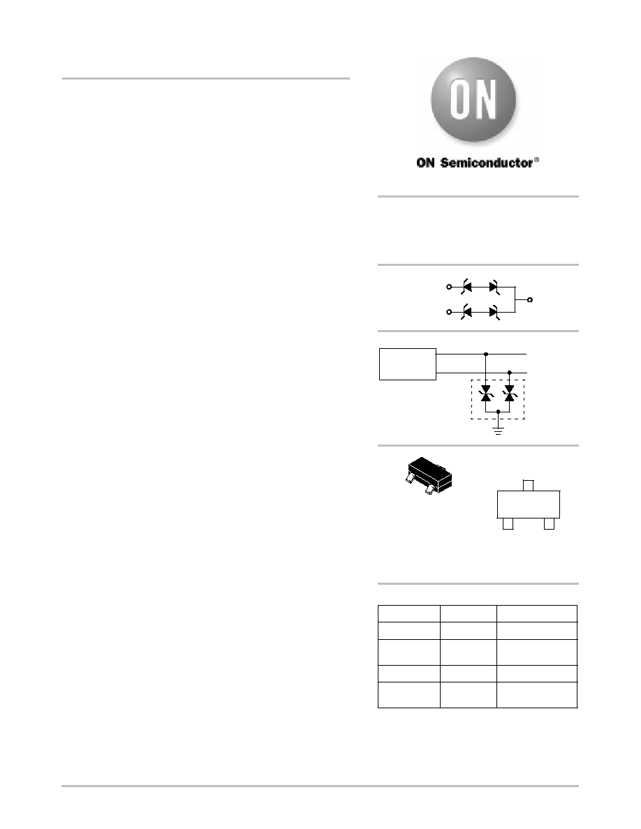
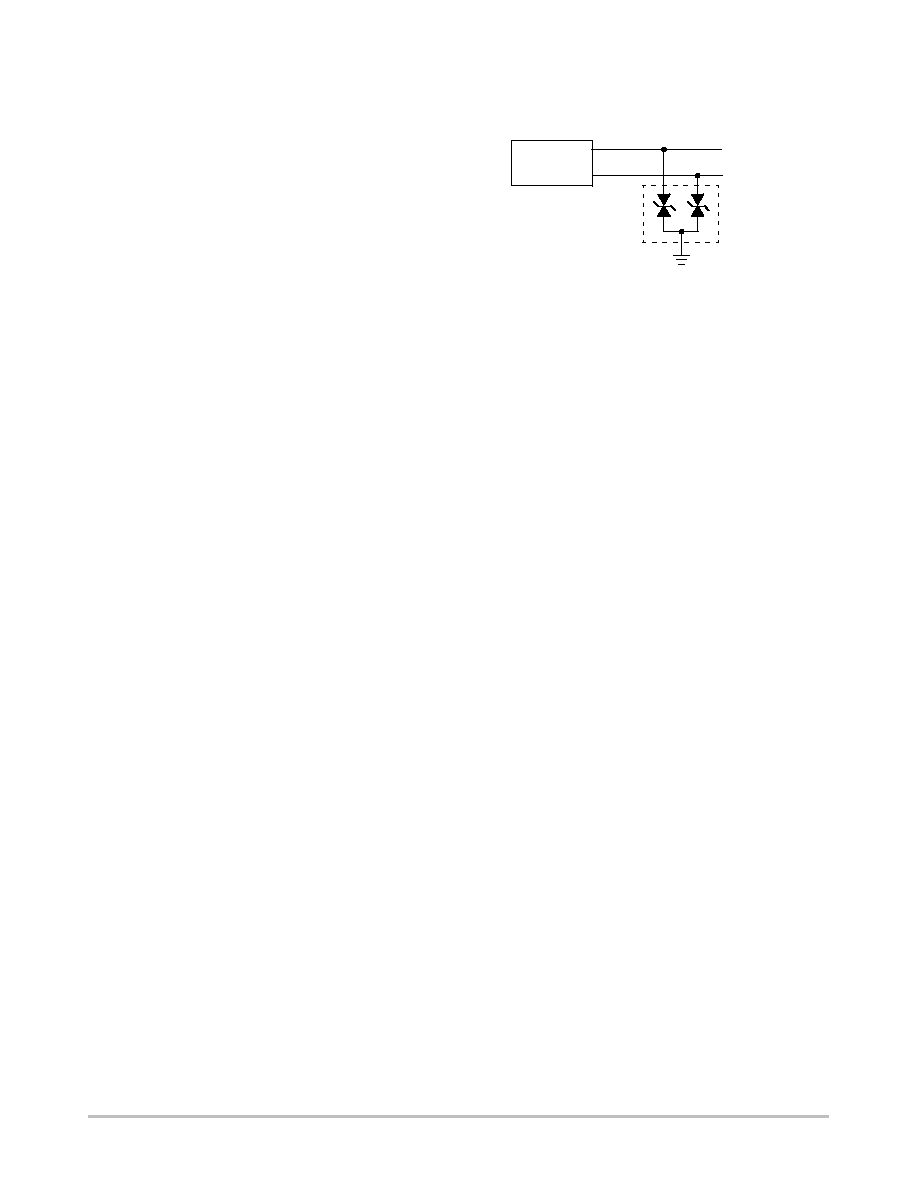
TVS Diode Protection Circuit
TVS diodes provide protection to a transceiver by
clamping a surge voltage to a safe level. TVS diodes have
high impedance below and low impedance above their
breakdown voltage. A TVS Zener diode has its junction
optimized to absorb the high peak energy of a transient
event, while a standard Zener diode is designed and
specified to clamp a steady state voltage.
Figure 7 provides an example of a dual bidirectional
TVS diode array that can be used for protection with the
high-speed CAN network. The bidirectional array is created
from four identical Zener TVS diodes. The clamping
voltage of the composite device is equal to the breakdown
voltage of the diode that is reversed biased, plus the diode
drop of the second diode that is forwarded biased.
Figure 7. High-Speed and Fault Tolerant CAN TVS
Protection Circuit
CAN
Transceiver
CAN_H
CAN_L
NUP2105L
CAN Bus

NUP2105L
http://onsemi.com
7
PACKAGE DIMENSIONS
mm
inches
SCALE 10:1
0.8
0.031
0.9
0.035
0.95
0.037
0.95
0.037
2.0
0.079
*For additional information on our Pb-Free strategy and soldering
details, please download the ON Semiconductor Soldering and
Mounting Techniques Reference Manual, SOLDERRM/D.
SOLDERING FOOTPRINT*
D
J
K
L
A
C
B S
H
G
V
3
1
2
DIM
A
MIN
MAX
MIN
MAX
MILLIMETERS
0.1102
0.1197
2.80
3.04
INCHES
B
0.0472
0.0551
1.20
1.40
C
0.0350
0.0440
0.89
1.11
D
0.0150
0.0200
0.37
0.50
G
0.0701
0.0807
1.78
2.04
H
0.0005
0.0040
0.013
0.100
J
0.0034
0.0070
0.085
0.177
K
0.0140
0.0285
0.35
0.69
L
0.0350
0.0401
0.89
1.02
S
0.0830
0.1039
2.10
2.64
V
0.0177
0.0236
0.45
0.60
SOT-23 (TO-236)
CASE 318-08
ISSUE AK
NOTES:
1. DIMENSIONING AND TOLERANCING PER ANSI
Y14.5M, 1982.
2. CONTROLLING DIMENSION: INCH.
3. MAXIMUM LEAD THICKNESS INCLUDES LEAD
FINISH THICKNESS. MINIMUM LEAD
THICKNESS IS THE MINIMUM THICKNESS OF
BASE MATERIAL.
4. 318-01 THRU -07 AND -09 OBSOLETE, NEW
STANDARD 318-08.
STYLE 27:
PIN 1. CATHODE
2. CATHODE
3. CATHODE

NUP2105L
http://onsemi.com
8
ON Semiconductor and are registered trademarks of Semiconductor Components Industries, LLC (SCILLC). SCILLC reserves the right to make changes without further notice
to any products herein. SCILLC makes no warranty, representation or guarantee regarding the suitability of its products for any particular purpose, nor does SCILLC assume any liability
arising out of the application or use of any product or circuit, and specifically disclaims any and all liability, including without limitation special, consequential or incidental damages.
"Typical" parameters which may be provided in SCILLC data sheets and/or specifications can and do vary in different applications and actual performance may vary over time. All
operating parameters, including "Typicals" must be validated for each customer application by customer's technical experts. SCILLC does not convey any license under its patent rights
nor the rights of others. SCILLC products are not designed, intended, or authorized for use as components in systems intended for surgical implant into the body, or other applications
intended to support or sustain life, or for any other application in which the failure of the SCILLC product could create a situation where personal injury or death may occur. Should
Buyer purchase or use SCILLC products for any such unintended or unauthorized application, Buyer shall indemnify and hold SCILLC and its officers, employees, subsidiaries, affiliates,
and distributors harmless against all claims, costs, damages, and expenses, and reasonable attorney fees arising out of, directly or indirectly, any claim of personal injury or death
associated with such unintended or unauthorized use, even if such claim alleges that SCILLC was negligent regarding the design or manufacture of the part. SCILLC is an Equal
Opportunity/Affirmative Action Employer. This literature is subject to all applicable copyright laws and is not for resale in any manner.
PUBLICATION ORDERING INFORMATION
N. American Technical Support: 800-282-9855 Toll Free
USA/Canada
Japan: ON Semiconductor, Japan Customer Focus Center
2-9-1 Kamimeguro, Meguro-ku, Tokyo, Japan 153-0051
Phone: 81-3-5773-3850
NUP2105L/D
Honeywell and SDS are registered trademarks of Honeywell International Inc.
DeviceNet is a trademark of Rockwell Automation.
LITERATURE FULFILLMENT:
Literature Distribution Center for ON Semiconductor
P.O. Box 61312, Phoenix, Arizona 85082-1312 USA
Phone: 480-829-7710 or 800-344-3860 Toll Free USA/Canada
Fax: 480-829-7709 or 800-344-3867 Toll Free USA/Canada
Email: orderlit@onsemi.com
ON Semiconductor Website: http://onsemi.com
Order Literature: http://www.onsemi.com/litorder
For additional information, please contact your
local Sales Representative.