 | –≠–ª–µ–∫—Ç—Ä–æ–Ω–Ω—ã–π –∫–æ–º–ø–æ–Ω–µ–Ω—Ç: NZF220TT1 | –°–∫–∞—á–∞—Ç—å:  PDF PDF  ZIP ZIP |

©
Semiconductor Components Industries, LLC, 2002
May, 2002 ≠ Rev. 2
1
Publication Order Number:
NZF220TT1/D
NZF220TT1
EMI Filter with ESD
Protection
Features:
∑
EMI/RFI Bi≠directional "Pi" Low≠Pass Filters
∑
ESD Protection Meets IEC61000≠4≠2
∑
Diode Capacitance: 7 ≠ 10 pF
∑
Zener/Resistor Line Capacitance: 22
±
20% pF
∑
Low Zener Diode Leakage: 1
mA Maximum
∑
Zener Breakdown Voltage; 6 ≠ 8 Volts
Benefits:
∑
Designed to suppress EMI/RFI Noise in Systems Subjected to
Electromagnetic Interference
∑
Small Package Size Minimizes Parasitic Inductance, Thus a More
"Ideal" Low Pass Filtering Response
Typical Applications:
∑
Cellular Phones
∑
Communication Systems
∑
Computers
∑
Portable Products with Input/Output Conductors
MAXIMUM RATINGS
Rating
Symbol
Value
Unit
Peak Power Dissipation (Note 1)
8
◊
20
m
s Pulse
P
PK
14
Watts
Maximum Junction Temperature
T
J
150
∞
C
1. All diodes under power
SC≠75
CASE 463
STYLE 4
Device
Package
Shipping
ORDERING INFORMATION
NZF220TT1
SC≠75
3000/Tape & Reel
1
2
CIRCUIT DESCRIPTION
X6 D
MARKING DIAGRAM
3
2
3
1
X6 = Specific Device Code
D = Date Code
http://onsemi.com
NZF220TT1
http://onsemi.com
2
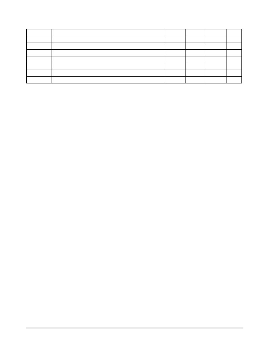
ELECTRICAL CHARACTERISTICS
Symbol
Characteristic
Min
Typ
Max
Unit
V
Z
Zener Breakdown Voltage, @ I
ZT
= 1 mA
6.0
≠
8.0
V
I
r
Zener Leakage Current, @ V
R
= 3 V
N/A
≠
1.0
m
A
V
F
Zener Forward Voltage, @ I
F
= 50 mA
N/A
≠
1.25
V
Capacitance
Zener Internal Capacitance, @ 0 V Bias
7.0
≠
10
pF
Capacitance
Zener/Resistor Array Line Capacitance
17.6
≠
26.4
pF
Resistor
Resistance
90
≠
110
W
F
C
(Note 2)
Cutoff Frequency
≠
220
≠
MHz
2. 50
W
Source and 50
W
Lead Termination per Figure 2
Applications Information
Suppressing Noise at the Source
∑
Filter all I/O signals leaving the noisy environment
∑
Locate I/O driver circuits close to the connector
∑
Use the longest rise/fall times possible for all digital signals
Reducing Noise at the Receiver
∑
Filter all I/O signals entering the unit
∑
Locate the I/O filters as close as possible to the connector
Minimizing Noise Coupling
∑
Use multilayer PCBs to minimize power and ground inductance
∑
Keep clock circuits away from the I/O connector
∑
Ground planes should be used whenever possible
∑
Minimize the loop area for all high speed signals
∑
Provide for adequate power decoupling
ESD Protection
∑
Locate the suppression devices as close to the I/O connector as possible
∑
Minimize the PCB trace length to the suppression device
∑
Minimize the PCB trace length for the ground return for the suppression device

NZF220TT1
http://onsemi.com
3
Frequency Response Specification
50
W
50
W
NZF220T
SPECTRUM
ANALYZER
TRACKING
GENERATOR
V
in
V
out
V
G
Test Conditions:
Source Impedance = 50
W
Load Impedance = 50
W
Input Power = 0 dB
TEST BOARD
TG OUTPUT
RF INPUT
Figure 1. Measurement Conditions
NZF220T
Figure 2. Typical EMI Filter Response
(50
W
Source and 50
W
Lead Termination)
GAIN (dB)
1.0
10
100
1000
f, FREQUENCY (MHz)
≠6.3
3000
≠50
OUTPUT
3 dB = 220 MHz
Y
Y

NZF220TT1
http://onsemi.com
4
OUTLINE DIMENSIONS
EMI Filter with ESD Protection
DIM
MIN
MAX
MIN
MAX
INCHES
MILLIMETERS
A
0.70
0.80
0.028
0.031
B
1.40
1.80
0.055
0.071
C
0.60
0.90
0.024
0.035
D
0.15
0.30
0.006
0.012
G
1.00 BSC
0.039 BSC
H
---
0.10
---
0.004
J
0.10
0.25
0.004
0.010
K
1.45
1.75
0.057
0.069
L
0.10
0.20
0.004
0.008
S
0.50 BSC
0.020 BSC
NOTES:
1. DIMENSIONING AND TOLERANCING PER ANSI
Y14.5M, 1982.
2. CONTROLLING DIMENSION: MILLIMETER.
M
0.20 (0.008)
B
≠A≠
≠B≠
S
D
G
3 PL
0.20 (0.008) A
K
J
L
C
H
3
2
1
STYLE 4:
PIN 1. CATHODE
2. CATHODE
3. ANODE
SC≠75/SOT≠416
CASE 463≠01
ISSUE B
ON Semiconductor and are registered trademarks of Semiconductor Components Industries, LLC (SCILLC). SCILLC reserves the right to make
changes without further notice to any products herein. SCILLC makes no warranty, representation or guarantee regarding the suitability of its products for any
particular purpose, nor does SCILLC assume any liability arising out of the application or use of any product or circuit, and specifically disclaims any and all
liability, including without limitation special, consequential or incidental damages. "Typical" parameters which may be provided in SCILLC data sheets and/or
specifications can and do vary in different applications and actual performance may vary over time. All operating parameters, including "Typicals" must be
validated for each customer application by customer's technical experts. SCILLC does not convey any license under its patent rights nor the rights of others.
SCILLC products are not designed, intended, or authorized for use as components in systems intended for surgical implant into the body, or other applications
intended to support or sustain life, or for any other application in which the failure of the SCILLC product could create a situation where personal injury or death
may occur. Should Buyer purchase or use SCILLC products for any such unintended or unauthorized application, Buyer shall indemnify and hold SCILLC
and its officers, employees, subsidiaries, affiliates, and distributors harmless against all claims, costs, damages, and expenses, and reasonable attorney fees
arising out of, directly or indirectly, any claim of personal injury or death associated with such unintended or unauthorized use, even if such claim alleges that
SCILLC was negligent regarding the design or manufacture of the part. SCILLC is an Equal Opportunity/Affirmative Action Employer.
PUBLICATION ORDERING INFORMATION
JAPAN: ON Semiconductor, Japan Customer Focus Center
4≠32≠1 Nishi≠Gotanda, Shinagawa≠ku, Tokyo, Japan 141≠0031
Phone: 81≠3≠5740≠2700
Email: r14525@onsemi.com
ON Semiconductor Website: http://onsemi.com
For additional information, please contact your local
Sales Representative.
NZF220TT1/D
Literature Fulfillment:
Literature Distribution Center for ON Semiconductor
P.O. Box 5163, Denver, Colorado 80217 USA
Phone: 303≠675≠2175 or 800≠344≠3860 Toll Free USA/Canada
Fax: 303≠675≠2176 or 800≠344≠3867 Toll Free USA/Canada
Email: ONlit@hibbertco.com
N. American Technical Support: 800≠282≠9855 Toll Free USA/Canada