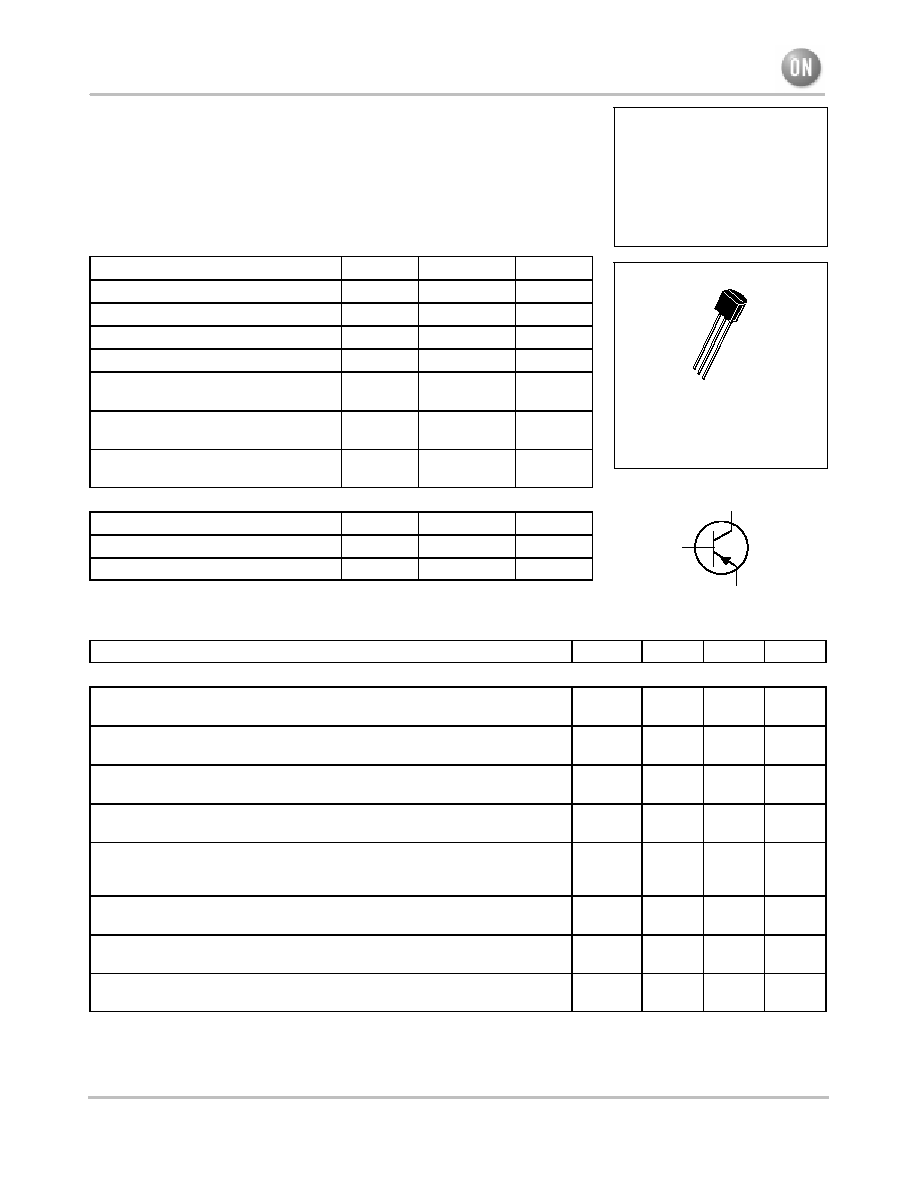
Amplifier Transistor
PNP Silicon
MAXIMUM RATINGS
Rating
Symbol
Value
Unit
Collector¡Emitter Voltage
V
CEO
¡60
Vdc
Collector¡Base Voltage
V
CBO
¡60
Vdc
Emitter¡Base Voltage
V
EBO
¡5.0
Vdc
Collector Current -- Continuous
I
C
¡600
mAdc
Total Device Dissipation @ T
A
= 25
░
C
Derate above 25
░
C
P
D
625
5.0
mW
mW/
░
C
Total Device Dissipation @ T
C
= 25
░
C
Derate above 25
░
C
P
D
1.5
12
Watts
mW/
░
C
Operating and Storage Junction
Temperature Range
T
J
, T
stg
¡55 to +150
░
C
THERMAL CHARACTERISTICS
Characteristic
Symbol
Max
Unit
Thermal Resistance, Junction to Ambient
R
q
JA
200
░
C/W
Thermal Resistance, Junction to Case
R
q
JC
83.3
░
C/W
ELECTRICAL CHARACTERISTICS
(T
A
= 25
░
C unless otherwise noted)
Characteristic
Symbol
Min
Max
Unit
OFF CHARACTERISTICS
Collector¡Emitter Breakdown Voltage
(1)
(I
C
= ¡10 mAdc, I
B
= 0)
V
(BR)CEO
¡60
--
Vdc
Collector¡Base Breakdown Voltage
(I
C
= ¡10
m
Adc, I
E
= 0)
V
(BR)CBO
¡60
--
Vdc
Emitter¡Base Breakdown Voltage
(I
E
= ¡10
m
Adc, I
C
= 0)
V
(BR)EBO
¡5.0
--
Vdc
Collector Cutoff Current
(V
CE
= ¡30 Vdc, V
EB(off)
= ¡0.5 Vdc)
I
CEX
--
¡50
nAdc
Collector Cutoff Current
(V
CB
= ¡50 Vdc, I
E
= 0)
(V
CB
= ¡50 Vdc, I
E
= 0, T
A
= 150
░
C)
I
CBO
--
--
¡0.01
¡10
╡
Adc
Emitter Cutoff Current
(V
EB
= ¡3.0 Vdc)
I
EBO
--
¡10
nAdc
Collector Cutoff Current
(V
CE
= ¡10 V)
I
CEO
--
¡10
nAdc
Base Cutoff Current
(V
CE
= ¡30 Vdc, V
EB(off)
= ¡0.5 Vdc)
I
BEX
--
¡50
nAdc
1. Pulse Test: Pulse Width
v
300
m
s, Duty Cycle
v
2.0%.
ON Semiconductort
⌐
Semiconductor Components Industries, LLC, 2001
March, 2001 ¡ Rev. 1
1
Publication Order Number:
P2N2907A/D
P2N2907A
CASE 29¡11, STYLE 17
TO¡92 (TO¡226AA)
1
2
3
COLLECTOR
1
2
BASE
3
EMITTER
P2N2907A
http://onsemi.com
2
ELECTRICAL CHARACTERISTICS
(T
A
= 25
░
C unless otherwise noted) (Continued)
Characteristic
Symbol
Min
Max
Unit
ON CHARACTERISTICS
DC Current Gain
(I
C
= ¡0.1 mAdc, V
CE
= ¡10 Vdc)
(I
C
= ¡1.0 mAdc, V
CE
= ¡10 Vdc)
(I
C
= ¡10 mAdc, V
CE
= ¡10 Vdc)
(I
C
= ¡150 mAdc, V
CE
= ¡10 Vdc)
(1)
(I
C
= ¡500 mAdc, V
CE
= ¡10 Vdc)
(1)
h
FE
75
100
100
100
50
--
--
--
300
--
--
Collector¡Emitter Saturation Voltage
(1)
(I
C
= ¡150 mAdc, I
B
= ¡15 mAdc)
(I
C
= ¡500 mAdc, I
B
= ¡50 mAdc)
V
CE(sat)
--
--
¡0.4
¡1.6
Vdc
Base¡Emitter Saturation Voltage
(1)
(I
C
= ¡150 mAdc, I
B
= ¡15 mAdc)
(I
C
= ¡500 mAdc, I
B
= ¡50 mAdc)
V
BE(sat)
--
--
¡1.3
¡2.6
Vdc
SMALL¡SIGNAL CHARACTERISTICS
Current¡Gain -- Bandwidth Product
(1), (2)
(I
C
= ¡50 mAdc, V
CE
= ¡20 Vdc, f = 100 MHz)
f
T
200
--
MHz
Output Capacitance
(V
CB
= ¡10 Vdc, I
E
= 0, f = 1.0 MHz)
C
obo
--
8.0
pF
Input Capacitance
(V
EB
= ¡2.0 Vdc, I
C
= 0, f = 1.0 MHz)
C
ibo
--
30
pF
SWITCHING CHARACTERISTICS
Turn¡On Time
(V
30 Vd
I
150
Ad
t
on
--
50
ns
Delay Time
(V
CC
= ¡30 Vdc, I
C
= ¡150 mAdc,
I
B1
= ¡15 mAdc) (Figures 1 and 5)
t
d
--
10
ns
Rise Time
I
B1
= ¡15 mAdc) (Figures 1 and 5)
t
r
--
40
ns
Turn¡Off Time
(V
6 0 Vd
I
150
Ad
t
off
--
110
ns
Storage Time
(V
CC
= ¡6.0 Vdc, I
C
= ¡150 mAdc,
I
B1
= I
B2
= ¡15 mAdc) (Figure 2)
t
s
--
80
ns
Fall Time
I
B1
= I
B2
= ¡15 mAdc) (Figure 2)
t
f
--
30
ns
1. Pulse Test: Pulse Width
v
300
m
s, Duty Cycle
v
2.0%.
2. f
T
is defined as the frequency at which |h
fe
| extrapolates to unity.
0
0
-16 V
200 ns
50
1.0 k
200
-30 V
TO OSCILLOSCOPE
RISE TIME
5.0 ns
+15 V -6.0 V
1.0 k
37
50
1N916
1.0 k
200 ns
-30 V
TO OSCILLOSCOPE
RISE TIME
5.0 ns
INPUT
Z
o
= 50
PRF = 150 PPS
RISE TIME
2.0 ns
P.W. < 200 ns
INPUT
Z
o
= 50
PRF = 150 PPS
RISE TIME
2.0 ns
P.W. < 200 ns
Figure 1. Delay and Rise Time Test Circuit
Figure 2. Storage and Fall Time Test Circuit
P2N2907A
http://onsemi.com
3
TYPICAL CHARACTERISTICS
Figure 3. DC Current Gain
I
C
, COLLECTOR CURRENT (mA)
0.3
0.5
0.7
1.0
3.0
0.2
-0.1
T
J
= 125
░
C
25
░
C
-55
░
C
V
CE
= -1.0 V
V
CE
= -10 V
h FE
, NORMALIZED CURRENT
GAIN
2.0
-0.2 -0.3
-0.5 -0.7 -1.0
-2.0 -3.0
-5.0 -7.0 -10
-20 -30
-50 -70 -100
-200 -300 -500
Figure 4. Collector Saturation Region
I
B
, BASE CURRENT (mA)
-0.4
-0.6
-0.8
-1.0
-0.2
V , COLLECT
OR-EMITTER VOL
T
AGE (VOL
TS)
0
CE
I
C
= -1.0 mA
-0.005
-10 mA
-0.01
-100 mA
-500 mA
-0.02 -0.03 -0.05 -0.07 -0.1
-0.2 -0.3
-0.5 -0.7 -1.0
-2.0 -3.0
-5.0 -7.0 -10
-20 -30
-50
Figure 5. Turn¡On Time
I
C
, COLLECTOR CURRENT
300
-5.0
Figure 6. Turn¡Off Time
I
C
, COLLECTOR CURRENT (mA)
-5.0
t, TIME
(ns)
t, TIME
(ns)
200
100
70
50
30
20
10
7.0
5.0
3.0
-7.0 -10
-20 -30
-50 -70 -100
-200 -300 -500
t
r
2.0 V
t
d
@ V
BE(off)
= 0 V
V
CC
= -30 V
I
C
/I
B
= 10
T
J
= 25
░
C
500
300
100
70
50
30
20
10
7.0
5.0
-7.0 -10
-20 -30
-50 -70 -100
-200 -300 -500
200
t
f
t
s
= t
s
- 1/8 t
f
V
CC
= -30 V
I
C
/I
B
= 10
I
B1
= I
B2
T
J
= 25
░
C
P2N2907A
http://onsemi.com
4
TYPICAL SMALL¡SIGNAL CHARACTERISTICS
NOISE FIGURE
V
CE
= 10 Vdc, T
A
= 25
░
C
Figure 7. Frequency Effects
f, FREQUENCY (kHz)
10
0.01
Figure 8. Source Resistance Effects
R
s
, SOURCE RESISTANCE (OHMS)
NF
, NOISE FIGURE (dB)
NF
, NOISE FIGURE (dB)
f = 1.0 kHz
I
C
= -50
╡
A
-100
╡
A
-500
╡
A
-1.0 mA
R
s
= OPTIMUM SOURCE RESISTANCE
8.0
6.0
4.0
2.0
0
0.02 0.05 0.1 0.2
0.5 1.0 2.0
5.0 10 20
50 100
10
8.0
6.0
4.0
2.0
0
50 100 200
500 1.0 k 2.0 k
5.0 k 10 k 20 k
50 k
I
C
= -1.0 mA, R
s
= 430
-500
╡
A, R
s
= 560
-50
╡
A, R
s
= 2.7 k
-100
╡
A, R
s
= 1.6 k
Figure 9. Capacitances
REVERSE VOLTAGE (VOLTS)
30
Figure 10. Current¡Gain -- Bandwidth Product
I
C
, COLLECTOR CURRENT (mA)
C, CAP
ACIT
ANCE (pF)
-0.1
2.0
Figure 11. "On" Voltage
I
C
, COLLECTOR CURRENT (mA)
-1.0
Figure 12. Temperature Coefficients
I
C
, COLLECTOR CURRENT (mA)
V
,
VOL
T
AGE (VOL
TS)
T
J
= 25
░
C
V
BE(sat)
@ I
C
/I
B
= 10
V
CE(sat)
@ I
C
/I
B
= 10
V
BE(on)
@ V
CE
= -10 V
R
qVC
for V
CE(sat)
f T
, CURRENT-GAIN BANDWIDTH PRODUCT
(MHz)
COEFFICIENT
(mV/
░
C)
20
10
7.0
5.0
3.0
-0.2 -0.3 -0.5
-1.0
-2.0 -3.0 -5.0
-10
-20
-30
400
300
200
100
80
60
40
30
20
-1.0 -2.0
-5.0 -10 -20
-50 -100 -200
-500 -1000
-0.8
-0.6
-0.4
-0.2
0
-0.1 -0.2 -0.5 -1.0 -2.0 -5.0 -10 -20 -50 -100 -200 -500
+0.5
0
-0.5
-1.0
-1.5
-2.0
-2.5
-0.1 -0.2 -0.5 -1.0 -2.0 -5.0 -10 -20 -50 -100 -200 -500
C
eb
C
cb
V
CE
= -20 V
T
J
= 25
░
C
R
qVB
for V
BE
P2N2907A
http://onsemi.com
5
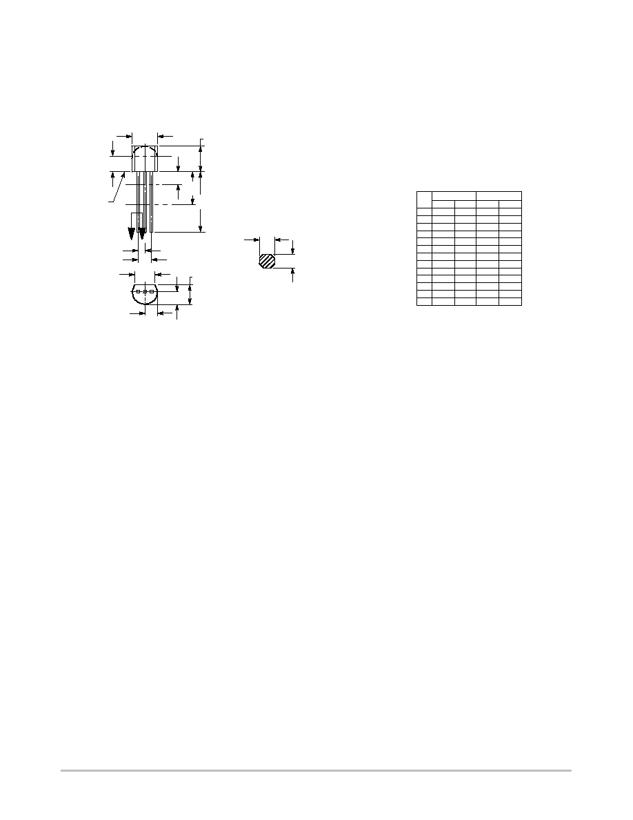
PACKAGE DIMENSIONS
CASE 29¡11
ISSUE AL
TO¡92 (TO¡226)
NOTES:
1. DIMENSIONING AND TOLERANCING PER ANSI
Y14.5M, 1982.
2. CONTROLLING DIMENSION: INCH.
3. CONTOUR OF PACKAGE BEYOND DIMENSION R
IS UNCONTROLLED.
4. LEAD DIMENSION IS UNCONTROLLED IN P AND
BEYOND DIMENSION K MINIMUM.
R
A
P
J
L
B
K
G
H
SECTION X¡X
C
V
D
N
N
X X
SEATING
PLANE
DIM
MIN
MAX
MIN
MAX
MILLIMETERS
INCHES
A
0.175
0.205
4.45
5.20
B
0.170
0.210
4.32
5.33
C
0.125
0.165
3.18
4.19
D
0.016
0.021
0.407
0.533
G
0.045
0.055
1.15
1.39
H
0.095
0.105
2.42
2.66
J
0.015
0.020
0.39
0.50
K
0.500
---
12.70
---
L
0.250
---
6.35
---
N
0.080
0.105
2.04
2.66
P
---
0.100
---
2.54
R
0.115
---
2.93
---
V
0.135
---
3.43
---
1
STYLE 1:
PIN 1. EMITTER
2. BASE
3. COLLECTOR

P2N2907A
http://onsemi.com
6
Notes

P2N2907A
http://onsemi.com
7
Notes

P2N2907A
http://onsemi.com
8
ON Semiconductor and are trademarks of Semiconductor Components Industries, LLC (SCILLC). SCILLC reserves the right to make changes
without further notice to any products herein. SCILLC makes no warranty, representation or guarantee regarding the suitability of its products for any particular
purpose, nor does SCILLC assume any liability arising out of the application or use of any product or circuit, and specifically disclaims any and all liability,
including without limitation special, consequential or incidental damages. "Typical" parameters which may be provided in SCILLC data sheets and/or
specifications can and do vary in different applications and actual performance may vary over time. All operating parameters, including "Typicals" must be
validated for each customer application by customer's technical experts. SCILLC does not convey any license under its patent rights nor the rights of others.
SCILLC products are not designed, intended, or authorized for use as components in systems intended for surgical implant into the body, or other applications
intended to support or sustain life, or for any other application in which the failure of the SCILLC product could create a situation where personal injury or
death may occur. Should Buyer purchase or use SCILLC products for any such unintended or unauthorized application, Buyer shall indemnify and hold
SCILLC and its officers, employees, subsidiaries, affiliates, and distributors harmless against all claims, costs, damages, and expenses, and reasonable
attorney fees arising out of, directly or indirectly, any claim of personal injury or death associated with such unintended or unauthorized use, even if such claim
alleges that SCILLC was negligent regarding the design or manufacture of the part. SCILLC is an Equal Opportunity/Affirmative Action Employer.
PUBLICATION ORDERING INFORMATION
CENTRAL/SOUTH AMERICA:
Spanish Phone: 303¡308¡7143 (Mon¡Fri 8:00am to 5:00pm MST)
Email: ONlit¡spanish@hibbertco.com
Toll¡Free from Mexico: Dial 01¡800¡288¡2872 for Access ¡
then Dial 866¡297¡9322
ASIA/PACIFIC: LDC for ON Semiconductor ¡ Asia Support
Phone: 1¡303¡675¡2121 (Tue¡Fri 9:00am to 1:00pm, Hong Kong Time)
Toll Free from Hong Kong & Singapore:
001¡800¡4422¡3781
Email: ONlit¡asia@hibbertco.com
JAPAN: ON Semiconductor, Japan Customer Focus Center
4¡32¡1 Nishi¡Gotanda, Shinagawa¡ku, Tokyo, Japan 141¡0031
Phone: 81¡3¡5740¡2700
Email: r14525@onsemi.com
ON Semiconductor Website: http://onsemi.com
For additional information, please contact your local
Sales Representative.
P2N2907A/D
NORTH AMERICA Literature Fulfillment:
Literature Distribution Center for ON Semiconductor
P.O. Box 5163, Denver, Colorado 80217 USA
Phone: 303¡675¡2175 or 800¡344¡3860 Toll Free USA/Canada
Fax: 303¡675¡2176 or 800¡344¡3867 Toll Free USA/Canada
Email: ONlit@hibbertco.com
Fax Response Line: 303¡675¡2167 or 800¡344¡3810 Toll Free USA/Canada
N. American Technical Support: 800¡282¡9855 Toll Free USA/Canada
EUROPE: LDC for ON Semiconductor ¡ European Support
German Phone: (+1) 303¡308¡7140 (Mon¡Fri 2:30pm to 7:00pm CET)
Email: ONlit¡german@hibbertco.com
French Phone: (+1) 303¡308¡7141 (Mon¡Fri 2:00pm to 7:00pm CET)
Email: ONlit¡french@hibbertco.com
English Phone: (+1) 303¡308¡7142 (Mon¡Fri 12:00pm to 5:00pm GMT)
Email: ONlit@hibbertco.com
EUROPEAN TOLL¡FREE ACCESS*: 00¡800¡4422¡3781
*Available from Germany, France, Italy, UK, Ireland