 | –≠–ª–µ–∫—Ç—Ä–æ–Ω–Ω—ã–π –∫–æ–º–ø–æ–Ω–µ–Ω—Ç: SG3526 | –°–∫–∞—á–∞—Ç—å:  PDF PDF  ZIP ZIP |
Device
Operating
Temperature Range
Package
SG3526
SEMICONDUCTOR
TECHNICAL DATA
PULSE WIDTH MODULATION
CONTROL CIRCUIT
ORDERING INFORMATION
SG3526N
TJ = 0
∞
to +125
∞
C
Plastic DIP
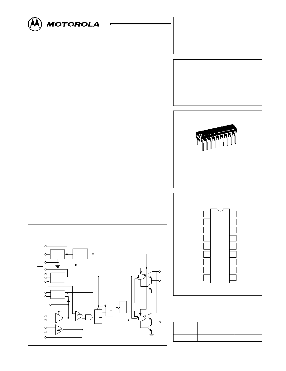
PIN CONNECTIONS
Order this document by SG3526/D
N SUFFIX
PLASTIC PACKAGE
CASE 707
18
1
(Top View)
+Error
Compensation
CSoft≠Start
≠CS
+CS
Shutdown
≠Error
Reset
RT
RDeadtime
Sync
Output A
Ground
Output B
VCC
Vref
VC
CT
1
2
3
4
5
6
7
8
12
13
14
15
16
17
18
9
11
10
1
MOTOROLA ANALOG IC DEVICE DATA
Pulse Width Modulation
Control Circuit
The SG3526 is a high performance pulse width modulator integrated
circuit intended for fixed frequency switching regulators and other power
control applications.
Functions included in this IC are a temperature compensated voltage
reference, sawtooth oscillator, error amplifier, pulse width modulator, pulse
metering and steering logic, and two high current totem pole outputs ideally
suited for driving the capacitance of power FETs at high speeds.
Additional protective features include soft start and undervoltage lockout,
digital current limiting, double pulse inhibit, adjustable dead time and a data
latch for single pulse metering. All digital control ports are TTL and B≠series
CMOS compatible. Active low logic design allows easy wired≠OR
connections for maximum flexibility. The versatility of this device enables
implementation in single≠ended or push≠pull switching regulators that are
transformerless or transformer coupled. The SG3526 is specified over a
junction temperature range of 0
∞
to +125
∞
C.
∑
8.0 V to 35 V Operation
∑
5.0 V
±
1% Trimmed Reference
∑
1.0 Hz to 400 kHz Oscillator Range
∑
Dual Source/Sink Current Outputs:
±
100 mA
∑
Digital Current Limiting
∑
Programmable Dead Time
∑
Undervoltage Lockout
∑
Single Pulse Metering
∑
Programmable Soft≠Start
∑
Wide Current Limit Common Mode Range
∑
Guaranteed 6 Unit Synchronization
Representative Block Diagram
Vref
VCC
Ground
Sync
RDeadtime
RT
CT
Reset
CSoft≠Start
Compensation
+Error
≠Error
+C.S.
≠C.S.
Shutdown
18
17
15
12
11
9
10
5
4
3
1
2
7
6
8
Reference
Regulator
Soft
Start
VCC
Amp
Under≠
Voltage
Lockout
Metering
F/F
Memory
F/F
Toggle
F/F
S
D
Q
Q
S
R Q
T
Q
Q
14
VC
13
Output
A
16
Output
B
To Internal
Circuitry
Oscillator
≠
≠
≠
+
+
+
©
Motorola, Inc. 1996
Rev 2

SG3526
2
MOTOROLA ANALOG IC DEVICE DATA
MAXIMUM RATINGS
(Note 1)
Rating
Symbol
Value
Unit
Supply Voltage
VCC
+40
Vdc
Collector Supply Voltage
VC
+40
Vdc
Logic Inputs
≠0.3 to +5.5
V
Analog Inputs
≠0.3 to VCC
V
Output Current, Source or Sink
IO
±
200
mA
Reference Load Current (VCC = 40 V, Note 2)
Iref
50
mA
Logic Sink Current
15
mA
Power Dissipation
TA = +25
∞
C (Note 3)
TC = +25
∞
C (Note 4)
PD
1000
3000
mW
Thermal Resistance Junction≠to≠Air
R
JA
100
∞
C/W
Thermal Resistance Junction≠to≠Case
R
JC
42
∞
C/W
Operating Junction Temperature
TJ
+150
∞
C
Storage Temperature Range
Tstg
≠65 to +150
∞
C
Lead Temperature (Soldering, 10 Seconds)
TSolder
±
300
∞
C
NOTES: 1. Values beyond which damage may occur.
2. Maximum junction temperature must be observed.
3. Derate at 10 mW/
∞
C for ambient temperatures above +50
∞
C.
4. Derate at 24 mW/
∞
C for case temperatures above +25
∞
C.
RECOMMENDED OPERATING CONDITIONS
Characteristics
Symbol
Min
Max
Unit
Supply Voltage
VCC
8.0
35
Vdc
Collector Supply Voltage
VC
4.5
35
Vdc
Output Sink/Source Current (Each Output)
IO
0
±
100
mA
Reference Load Current
Iref
0
20
mA
Oscillator Frequency Range
fosc
0.001
400
kHz
Oscillator Timing Resistor
RT
2.0
150
k
Oscillator Timing Capacitor
CT
0.001
20
µ
F
Available Deadtime Range (40 kHz)
≠
3.0
50
%
Operating Junction Temperature Range
TJ
0
+125
∞
C

SG3526
3
MOTOROLA ANALOG IC DEVICE DATA
ELECTRICAL CHARACTERISTICS
(VCC = +15 Vdc, TJ = Tlow to Thigh [Note 5], unless otherwise noted.)
Characteristics
Symbol
Min
Typ
Max
Unit
REFERENCE SECTION (Note 6)
Reference Output Voltage (TJ = +25
∞
C)
Vref
4.90
5.00
5.10
V
Line Regulation (+8.0 V
VCC
+35 V)
Regline
≠
10
30
mV
Load Regulation (0 mA
IL
20 mA)
Regload
≠
10
50
mV
Temperature Stability
Vref/
T
≠
10
≠
mV
Total Reference Output Voltage Variation
(+8.0 V
VCC
+35 V, 0 mA
IL
20 mA)
Vref
4.85
5.00
5.15
V
Short Circuit Current (Vref = 0 V) (Note 2)
ISC
25
80
125
mA
UNDERVOLTAGE LOCKOUT
Reset Output Voltage (Vref = +3.8 V)
≠
0.2
0.4
V
Reset Output Voltage (Vref = +4.8 V)
2.4
4.8
≠
V
OSCILLATOR SECTION (Note 7)
Initial Accuracy (TJ = +25
∞
C)
≠
±
3.0
±
8.0
%
Frequency Stability over Power Supply Range
(+8.0 V
VCC
+35 V)
fosc
VCC
≠
0.5
1.0
%
Frequency Stability over Temperature
(
TJ = Tlow to Thigh)
fosc
TJ
≠
2.0
≠
%
Minimum Frequency
(RT = 150 k
, CT = 20
µ
F)
fmin
≠
0.5
≠
Hz
Maximum Frequency
(RT = 2.0 k
, CT = 0.001
µ
F)
fmax
400
≠
≠
kHz
Sawtooth Peak Voltage (VCC = +35 V)
Vosc(P)
≠
3.0
3.5
V
Sawtooth Valley Voltage (VCC = +8.0 V)
Vosc(V)
0.45
0.8
≠
V
ERROR AMPLIFIER SECTION (Note 8)
Input Offset Voltage (RS
2.0 k
)
VIO
≠
2.0
10
mV
Input Bias Current
IIB
≠
≠350
≠2000
nA
Input Offset Current
IIO
≠
35
200
nA
DC Open Loop Gain (RL
10 M
)
AVOL
60
72
≠
dB
High Output Voltage
(VPin 1≠VPin 2
+150 mV, Isource = 100
µ
A)
VOH
3.6
4.2
≠
V
Low Output Voltage
(VPin 2≠VPin 1
+150 mV, Isink = 100
µ
A)
VOL
≠
0.2
0.4
V
Common Mode Rejection Ratio (RS
2.0 k
)
CMRR
70
94
≠
dB
Power Supply Rejection Ratio (+12 V
VCC
+18 V)
PSRR
66
80
≠
dB
NOTES: 2. Maximum junction temperature must be observed.
5. Tlow = 0
∞
C
Thigh = +125
∞
C
6. IL = 0 mA unless otherwise noted.
7. fosc = 40 kHz (RT = 4.12 k
±
1%, CT = 0.01
µ
F
±
1%, RD = 0
)
8. 0 V
VCM
+5.2 V.

SG3526
4
MOTOROLA ANALOG IC DEVICE DATA
ELECTRICAL CHARACTERISTICS (continued)
Characteristics
Symbol
Min
Typ
Max
Unit
PWM COMPARATOR SECTION (Note 7)
Minimum Duty Cycle
(VCompensation = +0.4 V)
DCmin
≠
≠
0
%
Maximum Duty Cycle
(VCompensation = +3.6 V)
DCmax
45
49
≠
%
DIGITAL PORTS (SYNC, SHUTDOWN, RESET)
Output Voltage
(High Logic Level) (Isource = 40
µ
A)
(Low Logic Level) (Isink = 3.6 mA)
VOH
VOL
2.4
≠
4.0
0.2
≠
0.4
V
Input Current
High Logic Level
(High Logic Level) (VIH = +2.4 V)
(Low Logic Level) (VIL = +0.4 V)
IIH
IIL
≠
≠
≠125
≠225
≠200
≠360
µ
A
CURRENT LIMIT COMPARATOR SECTION (Note 9)
Sense Voltage (RS
50
)
Vsense
80
100
120
mA
Input Bias Current
IIB
≠3.0
≠10
µ
A
SOFT≠START SECTION
Error Clamp Voltage (Reset = +0.4 V)
≠
0.1
0.4
V
CSoft≠Start Charging Current (Reset = +2.4 V)
ICS
50
100
150
µ
A
OUTPUT DRIVERS (Each Output, VC = +15 Vdc, unless otherwise noted.)
Output High Level
Isource = 20 mA
Isource = 100 mA
VOH
12.5
12
13.5
13
≠
≠
V
Output Low Level
Isink = 20 mA
Isink = 100 mA
VOL
≠
≠
0.2
1.2
0.3
2.0
V
Collector Leakage, VC = +40 V
IC(leak)
≠
50
150
µ
A
Rise Time (CL = 1000 pF)
tr
≠
0.3
0.6
µ
s
Fall Time (CL = 1000 pF)
tf
≠
0.1
0.2
µ
s
Supply Current
(Shutdown = +0.4 V, VCC = +35 V, RT = 4.12 k
)
ICC
≠
18
30
mA
NOTES: 7. fosc = 40 kHz (RT = 4.12 k
±
1%, CT = 0.01
µ
F
±
1%, RD = 0
)
8. 0 V
VCM
+5.2 V
9. 0 V
VCM
+12 V
SG3526
5
MOTOROLA ANALOG IC DEVICE DATA
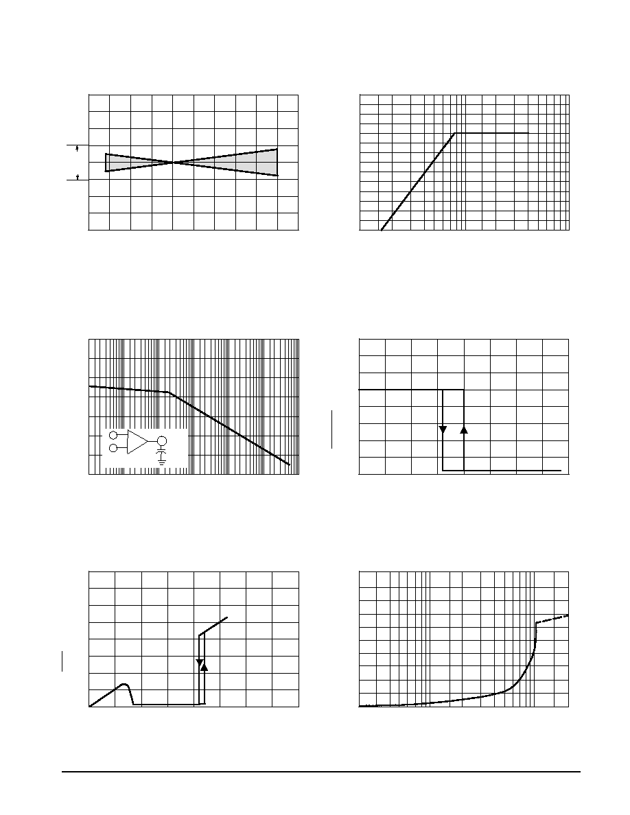
Figure 1. Reference Stability over Temperature
Figure 2. Reference Voltage as a
Function Supply Voltage
Figure 3. Error Amplifier Open Loop
Frequency Response
Figure 4. Current Limit Comparator Threshold
Figure 5. Undervoltage Lockout Characteristic
Figure 6. Output Driver Saturation Voltage as a
Function of Sink Current
≠75
≠50
≠25
0
25
50
75
100
125
150
TJ, JUNCTION TEMPERATURE (
∞
C)
50 mV
Spec
Limit
1.0
2.0
3.0 4.0 5.0
10
20
30 40
VCC, SUPPLY VOLTAGE (V)
, REFERENCE VOL
T
AGE (V)
ref
V
1
2
3
+
_
10
100
1.0 k
10 k
100 k
1.0 M
10 M
100 pF
CComp
f, FREQUENCY (Hz)
,
VOL
T
AGE GAIN (dB)
Vo
l
A
25
50
75
100
125
150
175
200
DIFFERENTIAL INPUT VOLTAGE (mV)
SHUTDOWN VOL
T
AGE (V)
0
1.0
2.0
3.0
4.0
5.0
6.0
7.0
8.0
Vref, REFERENCE VOLTAGE (V)
RESET
VOL
T
AGE
(V)
2.0
5.0
10
20
50
100
200
OUTPUT DRIVER SINK CURRENT (mA)
, OUTPUT
DRIVER SA
TURA
TION VOL
T
AGE (V)
sat
V
5.0
4.0
3.0
2.0
1.0
80
60
40
20
0
8.0
7.0
6.0
5.0
4.0
3.0
2.0
1.0
0
8.0
7.0
6.0
5.0
4.0
3.0
2.0
1.0
0
2.5
2.0
1.5
1.0
0.5
0

SG3526
6
MOTOROLA ANALOG IC DEVICE DATA
R
T
, TIMING RESIST
OR
(k
)
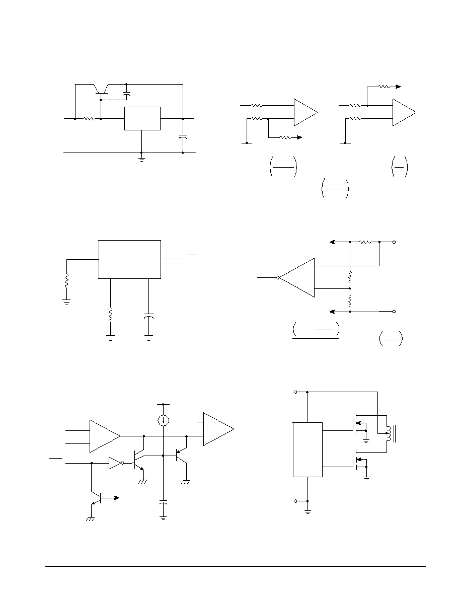
Figure 7. VC Saturation Voltage as a
Function of Sink Current
Figure 8. Oscillator Period
Figure 9. Error Amplifier
Figure 10. Undervoltage Lockout
Figure 11. Pulse Processing Logic
The metering Flip≠Flop is an asynchronous data latch
which suppresses high frequency oscillations by allowing
only one PWM pulse per oscillator cycle.
The memory Flip≠Flop prevents double pulsing in a
push≠pull configuration by remembering which output
produced the last pulse.
2.0
5.0
10
20
50
100
200
IC, SINK CURRENT (mA)
, SA
TURA
TION VOL
T
AGE
(V)
SA
T
V
0.002
0.005
0.01
0.02
0.05
0.1
0.2
0.5
1.0
2.0
5.0
10
20
50
100
200
500
1000
OSCILLATOR PERIOD (ms)
RD = 0
VCC
Q6
Q5
Vref
125
µ
A
Q3
Q4
50
µ
A
Q8
Q9
500
1.0k
Q2
1
+ Error
≠ Error
Q10
3 Compensation
Q12
Q11
Q7
50
µ
A
14
µ
A
Q1
1.0k
500
100
µ
A
14
µ
A
100
µ
A
100
µ
A
Vref
R1
1.2V
Bandgap
Reference
R2
+
≠
To Reset
To Driver A
To Driver B
Metering
F/F
S
D
Q
Q
Q
R
S
Clock
PWM
PWM
Sync
Memory
F/F
2.5
2.0
1.5
1.0
0.5
0
200
100
50
20
10
5.0
2.0
SG3526
7
MOTOROLA ANALOG IC DEVICE DATA
Figure 12. Extending Reference
Output Current Capability
Figure 13. Error Amplifier Connections
Figure 14. Oscillator Connections
Figure 15. Foldback Current Limiting
Figure 16. Soft≠Start Circuity
Figure 17. Driving VMOS Power FETs
The totem pole output drivers of the SG3526 are ideally
suited for driving the input capacitance of power FETs at
high speeds.
Reference
Regulator
17
18
C*
27
VCC
Gnd
Vref
+
10
µ
F
* May be required with some types of transistors
15
Gnd
Vref
R3
R2
1
2
R1
Positive
Output
Voltage
Gnd
Vref
R2
R3
R1
1
2
Vout = Vref
R1
+
≠
+
≠
Negative
Output
Voltage
Vout = Vref
R1 + R2
R3 =
R1R2
11
RD
9
10
12
SG3526
RT
CT
Sync
+
≠
Gnd
8
6
7
≠
R1
R2
RS
Output Filter
Vout
I(max) =
RS
0.1 V +
Vout R1
+
ISC =
0.1 V
RS
+
Error
Amp
≠
≠
+
PWM
Ramp
Vref
100
µ
A
Q2
Q1
To
Undervoltage
Lockout
CSoft≠Start
Q3
1
2
5
+ Error
≠ Error
Reset
+12V
14
13
16
VC
A
B
Gnd
SG3526
APPLICATIONS INFORMATION
R1 + R2
R2
R2
R1 + R2
SG3526
8
MOTOROLA ANALOG IC DEVICE DATA
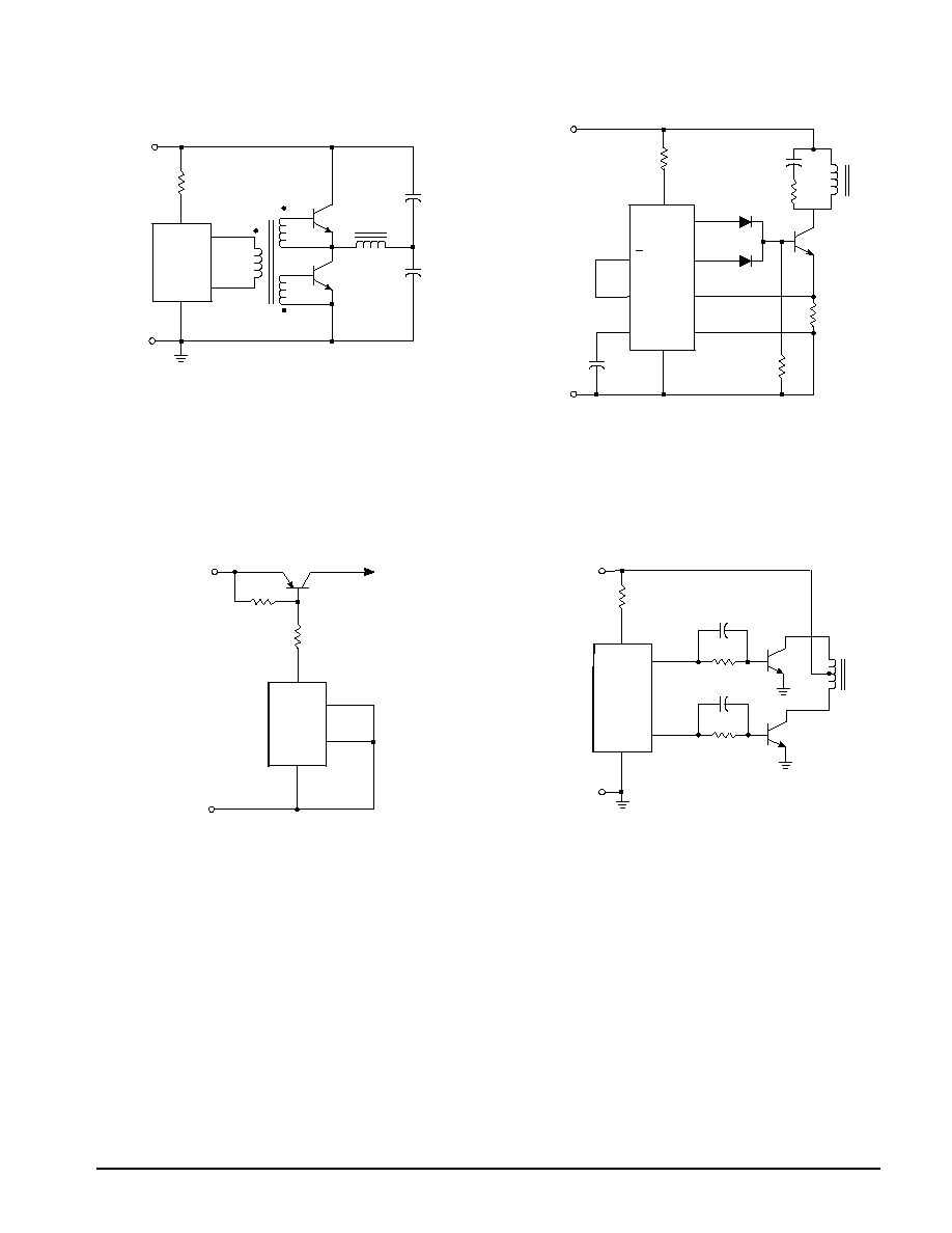
Figure 18. Half≠Bridge Configuration
Figure 19. Flyback Converter with
Current Limiting
Figure 20. Single≠Ended Configuration
Figure 21. Push≠Pull Configuration
+V
Supply
VC A
B
SG3526
Gnd
15
14
R1
13
16
Q2
Q1
T2
C2
T1
C1
In the above circuit, current limiting is accomplished by using the
current limit comparator output to reset the soft≠start capacitor.
+V
Supply
R1
C1
15
R2
R3
13
16
7
6
5
8
4
D1
D2
14
C2
R4
T1
Q1
VC
A
B
+CS
≠CS
Gnd
CS
S
R
SG3526
To
Output
Filter
Q1
R1
R2
14
13
16
VC
A
B
SG3526
Gnd
15
+V Supply
+V Supply
R1
14
15
VC
A
B
SG3526
Gnd
13
16
C1
R2
C2
R3
Q1
T1
Q2

SG3526
9
MOTOROLA ANALOG IC DEVICE DATA
OUTLINE DIMENSIONS
N SUFFIX
PLASTIC PACKAGE
CASE 707≠02
ISSUE C
NOTES:
1. POSITIONAL TOLERANCE OF LEADS (D),
SHALL BE WITHIN 0.25 (0.010) AT MAXIMUM
MATERIAL CONDITION, IN RELATION TO
SEATING PLANE AND EACH OTHER.
2. DIMENSION L TO CENTER OF LEADS WHEN
FORMED PARALLEL.
3. DIMENSION B DOES NOT INCLUDE MOLD
FLASH.
1
SEATING
PLANE
10
9
18
M
A
B
K
C
N
F
G
D
H
J
L
DIM
MIN
MAX
MIN
MAX
INCHES
MILLIMETERS
A
22.22
23.24
0.875
0.915
B
6.10
6.60
0.240
0.260
C
3.56
4.57
0.140
0.180
D
0.36
0.56
0.014
0.022
F
1.27
1.78
0.050
0.070
G
2.54 BSC
0.100 BSC
H
1.02
1.52
0.040
0.060
J
0.20
0.30
0.008
0.012
K
2.92
3.43
0.115
0.135
L
7.62 BSC
0.300 BSC
M
0
15
0
15
N
0.51
1.02
0.020
0.040
_
_
_
_
SG3526
10
MOTOROLA ANALOG IC DEVICE DATA
Motorola reserves the right to make changes without further notice to any products herein. Motorola makes no warranty, representation or guarantee regarding
the suitability of its products for any particular purpose, nor does Motorola assume any liability arising out of the application or use of any product or circuit, and
specifically disclaims any and all liability, including without limitation consequential or incidental damages. "Typical" parameters which may be provided in Motorola
data sheets and/or specifications can and do vary in different applications and actual performance may vary over time. All operating parameters, including "Typicals"
must be validated for each customer application by customer's technical experts. Motorola does not convey any license under its patent rights nor the rights of
others. Motorola products are not designed, intended, or authorized for use as components in systems intended for surgical implant into the body, or other
applications intended to support or sustain life, or for any other application in which the failure of the Motorola product could create a situation where personal injury
or death may occur. Should Buyer purchase or use Motorola products for any such unintended or unauthorized application, Buyer shall indemnify and hold Motorola
and its officers, employees, subsidiaries, affiliates, and distributors harmless against all claims, costs, damages, and expenses, and reasonable attorney fees
arising out of, directly or indirectly, any claim of personal injury or death associated with such unintended or unauthorized use, even if such claim alleges that Motorola
was negligent regarding the design or manufacture of the part. Motorola and are registered trademarks of Motorola, Inc. Motorola, Inc. is an Equal
Opportunity/Affirmative Action Employer.
How to reach us:
USA / EUROPE / Locations Not Listed: Motorola Literature Distribution;
JAPAN: Nippon Motorola Ltd.; Tatsumi≠SPD≠JLDC, 6F Seibu≠Butsuryu≠Center,
P.O. Box 20912; Phoenix, Arizona 85036. 1≠800≠441≠2447 or 602≠303≠5454
3≠14≠2 Tatsumi Koto≠Ku, Tokyo 135, Japan. 03≠81≠3521≠8315
MFAX: RMFAX0@email.sps.mot.com ≠ TOUCHTONE 602≠244≠6609
ASIA/PACIFIC: Motorola Semiconductors H.K. Ltd.; 8B Tai Ping Industrial Park,
INTERNET: http://Design≠NET.com
51 Ting Kok Road, Tai Po, N.T., Hong Kong. 852≠26629298
SG3526/D
*SG3526/D*