
©
Semiconductor Components Industries, LLC, 2001
October, 2001 ≠ Rev. 1
1
Publication Order Number:
SN74LS161A/D
SN74LS161A, SN74LS163A
BCD Decade Counters/
4-Bit Binary Counters
The LS161A/163A are high-speed 4-bit synchronous counters.
They are edge-triggered, synchronously presettable, and cascadable
MSI building blocks for counting, memory addressing, frequency
division and other applications. The LS161A and LS163A count
modulo 16 (binary).
The LS161A has an asynchronous Master Reset (Clear) input that
overrides, and is independent of, the clock and all other control inputs.
The LS163A has a Synchronous Reset (Clear) input that overrides all
other control inputs, but is active only during the rising clock edge.
Binary (Modulo 16)
Asynchronous Reset
LS161A
Synchronous Reset
LS163A
∑
Synchronous Counting and Loading
∑
Two Count Enable Inputs for High Speed Synchronous Expansion
∑
Terminal Count Fully Decoded
∑
Edge-Triggered Operation
∑
Typical Count Rate of 35 MHz
∑
ESD > 3500 Volts
GUARANTEED OPERATING RANGES
Symbol
Parameter
Min
Typ
Max
Unit
VCC
Supply Voltage
4.75
5.0
5.25
V
TA
Operating Ambient
Temperature Range
0
25
70
∞
C
IOH
Output Current ≠ High
≠0.4
mA
IOL
Output Current ≠ Low
8.0
mA
LOW
POWER
SCHOTTKY
SOIC
D SUFFIX
CASE 751B
PLASTIC
N SUFFIX
CASE 648
16
1
16
1
SOEIAJ
M SUFFIX
CASE 966
16
1
Device
Package
Shipping
ORDERING INFORMATION
SN74LS161AN
16 Pin DIP
2000 Units/Box
SN74LS161AD
SOIC≠16
38 Units/Rail
SN74LS161ADR2
SOIC≠16
2500/Tape & Reel
SN74LS161AM
SOEIAJ≠16
See Note 1
SN74LS161AMEL
SOEIAJ≠16
1. For ordering information on the EIAJ version of
the SOIC package, please contact your local
ON Semiconductor representative.
See Note 1
http://onsemi.com
16 Pin DIP
2000 Units/Box
SN74LS163AD
SOIC≠16
38 Units/Rail
SN74LS163ADR2
SOIC≠16
2500/Tape & Reel
SN74LS163AM
SOEIAJ≠16
See Note 1
SN74LS163AMEL
SOEIAJ≠16
See Note 1
SN74LS163AN
SN74LS161A, SN74LS163A
http://onsemi.com
2
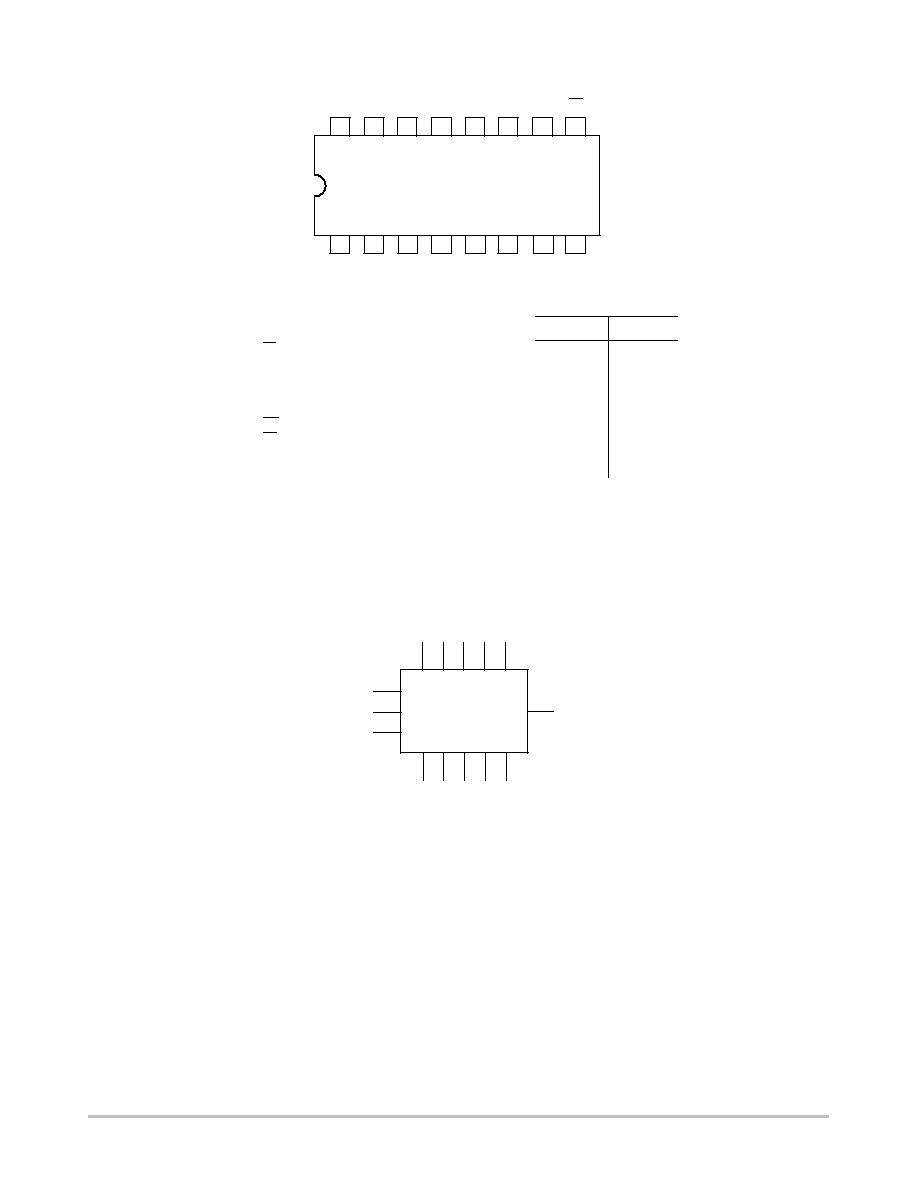
CONNECTION DIAGRAM DIP (TOP VIEW)
Parallel Enable (Active LOW) Input
Parallel Inputs
Count Enable Parallel Input
Count Enable Trickle Input
Clock (Active HIGH Going Edge) Input
Master Reset (Active LOW) Input
Synchronous Reset (Active LOW) Input
Parallel Outputs
Terminal Count Output
PE
P0 - P3
CEP
CET
CP
MR
SR
Q0 - Q3
TC
1.0 U.L.
0.5 U.L.
0.5 U.L.
1.0 U.L.
0.5 U.L.
0.5 U.L.
1.0 U.L.
10 U.L.
10 U.L.
0.5 U.L.
0.25 U.L.
0.25 U.L.
0.5 U.L.
0.25 U.L.
0.25 U.L.
0.5 U.L.
5 U.L.
5 U.L.
NOTES:
a) 1 TTL Unit Load (U.L.) = 40 mA HIGH/1.6 mA LOW.
HIGH
LOW
(Note a)
LOADING
PIN NAMES
VCC = PIN 16
GND = PIN 8
LOGIC SYMBOL
NOTE:
The Flatpak version has the same
pinouts (Connection Diagram) as
the Dual In Line Package.
14
13
12
11
10
9
1
2
3
4
5
6
7
16
15
8
VCC
*R
TC
Q0
Q1
Q2
CET
Q3
PE
CP
P0
P1
P2
P3
CEP GND
9 3 4
5 6
7
10
2
15
1 14 13 12 11
PE P0 P1 P2 P3
CEP
CET
CP
*R Q0 Q1 Q2 Q3
TC
*MR for LS161A
*SR for LS163A
*MR for LS161A
*SR for LS163A
SN74LS161A, SN74LS163A
http://onsemi.com
3
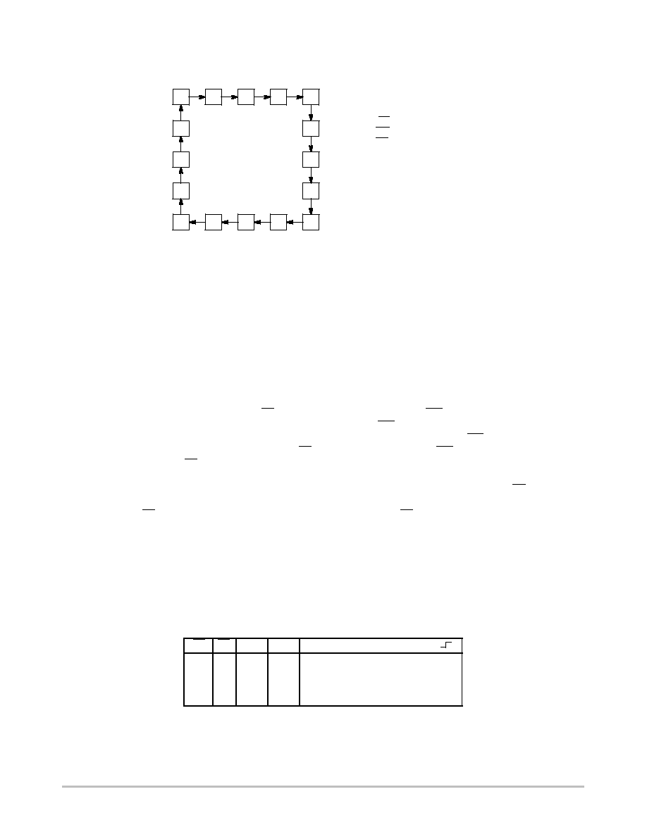
LS161A
∑
LS163A
0
1
2
3
4
5
6
7
8
9
10
11
12
13
14
15
Count Enable = CEP
∑
CET
∑
PE
TC for LS161A & LS163A = CET
∑
Q0
∑
Q1
∑
Q2
∑
Q3
Preset = PE
∑
CP + (rising clock edge)
Reset = MR (LS161A)
Reset = SR
∑
CP + (rising clock edge)
Reset =
(LS163A)
STATE DIAGRAM
LOGIC EQUATIONS
FUNCTIONAL DESCRIPTION
The LS161A/163A are 4-bit synchronous counters with a
synchronous Parallel Enable (Load) feature. The counters
consist of four edge-triggered D flip-flops with the
appropriate data routing networks feeding the D inputs. All
changes of the Q outputs (except due to the asynchronous
Master Reset in the LS161A) occur as a result of, and
synchronous with, the LOW to HIGH transition of the Clock
input (CP). As long as the set-up time requirements are met,
there are no special timing or activity constraints on any of
the mode control or data inputs.
Three control inputs -- Parallel Enable (PE), Count
Enable Parallel (CEP) and Count Enable Trickle (CET) --
select the mode of operation as shown in the tables below.
The Count Mode is enabled when the CEP, CET, and PE
inputs are HIGH. When the PE is LOW, the counters will
synchronously load the data from the parallel inputs into the
flip-flops on the LOW to HIGH transition of the clock.
Either the CEP or CET can be used to inhibit the count
sequence. With the PE held HIGH, a LOW on either the CEP
or CET inputs at least one set-up time prior to the LOW to
HIGH clock transition will cause the existing output states
to be retained. The AND feature of the two Count Enable
inputs (CET
∑
CEP) allows synchronous cascading without
external gating and without delay accumulation over any
practical number of bits or digits.
The Terminal Count (TC) output is HIGH when the Count
Enable Trickle (CET) input is HIGH while the counter is in
its maximum count state (HLLH for the BCD counters,
HHHH for the Binary counters). Note that TC is fully
decoded and will, therefore, be HIGH only for one count
state.
The LS161A and LS163A count modulo 16 following a
binary sequence. They generate a TC when the CET input is
HIGH while the counter is in state 15 (HHHH). From this
state they increment to state 0 (LLLL).
The Master Reset (MR) of the LS161A is asynchronous.
When the MR is LOW, it overrides all other input conditions
and sets the outputs LOW. The MR pin should never be left
open. If not used, the MR pin should be tied through a
resistor to VCC, or to a gate output which is permanently set
to a HIGH logic level.
The active LOW Synchronous Reset (SR) input of the
LS163A acts as an edge-triggered control input, overriding
CET, CEP and PE, and resetting the four counter flip-flops
on the LOW to HIGH transition of the clock. This simplifies
the design from race-free logic controlled reset circuits, e.g.,
to reset the counter synchronously after reaching a
predetermined value.
MODE SELECT TABLE
*SR
PE
CET
CEP
Action on the Rising Clock Edge ( )
L
X
X
X
RESET (Clear)
H
L
X
X
LOAD (Pn
Qn)
H
H
H
H
COUNT (Increment)
H
H
L
X
NO CHANGE (Hold)
H
H
X
L
NO CHANGE (Hold)
*For the LS163A only.
H = HIGH Voltage Level
L = LOW Voltage Level
X = Don't Care
SN74LS161A, SN74LS163A
http://onsemi.com
4
LS161A
DC CHARACTERISTICS OVER OPERATING TEMPERATURE RANGE
(unless otherwise specified)
Limits
Symbol
Parameter
Min
Typ
Max
Unit
Test Conditions
VIH
Input HIGH Voltage
2.0
V
Guaranteed Input HIGH Voltage for
All Inputs
VIL
Input LOW Voltage
0.8
V
Guaranteed Input LOW Voltage for
All Inputs
VIK
Input Clamp Diode Voltage
≠0.65
≠1.5
V
VCC = MIN, IIN = ≠18 mA
VOH
Output HIGH Voltage
2.7
3.5
V
VCC = MIN, IOH = MAX, VIN = VIH
or VIL per Truth Table
V
Output LOW Voltage
0.25
0.4
V
IOL = 4.0 mA
VCC = VCC MIN,
VIN VIL or VIH
VOL
Output LOW Voltage
0.35
0.5
V
IOL = 8.0 mA
VIN = VIL or VIH
per Truth Table
IIH
Input HIGH Current
MR, Data, CEP, Clock
PE, CET
20
40
µ
A
VCC = MAX, VIN = 2.7 V
IIH
MR, Data, CEP, Clock
PE, CET
0.1
0.2
mA
VCC = MAX, VIN = 7.0 V
IIL
Input LOW Current
MR, Data, CEP, Clock
PE, CET
≠0.4
≠0.8
mA
VCC = MAX, VIN = 0.4 V
IOS
Short Circuit Current (Note 2)
≠20
≠100
mA
VCC = MAX
ICC
Power Supply Current
Total, Output HIGH
Total, Output LOW
31
32
mA
VCC = MAX
2. Not more than one output should be shorted at a time, nor for more than 1 second.
LS163A
DC CHARACTERISTICS OVER OPERATING TEMPERATURE RANGE
(unless otherwise specified)
Limits
Symbol
Parameter
Min
Typ
Max
Unit
Test Conditions
VIH
Input HIGH Voltage
2.0
V
Guaranteed Input HIGH Voltage for
All Inputs
VIL
Input LOW Voltage
0.8
V
Guaranteed Input LOW Voltage for
All Inputs
VIK
Input Clamp Diode Voltage
≠0.65
≠1.5
V
VCC = MIN, IIN = ≠18 mA
VOH
Output HIGH Voltage
2.7
3.5
V
VCC = MIN, IOH = MAX, VIN = VIH
or VIL per Truth Table
V
Output LOW Voltage
0.25
0.4
V
IOL = 4.0 mA
VCC = VCC MIN,
VIN VIL or VIH
VOL
Output LOW Voltage
0.35
0.5
V
IOL = 8.0 mA
VIN = VIL or VIH
per Truth Table
IIH
Input HIGH Current
Data, CEP, Clock
PE, CET, SR
20
40
µ
A
VCC = MAX, VIN = 2.7 V
IIH
Data, CEP, Clock
PE, CET, SR
0.1
0.2
mA
VCC = MAX, VIN = 7.0 V
IIL
Input LOW Current
Data, CEP, Clock, PE, SR
CET
≠0.4
≠0.8
mA
VCC = MAX, VIN = 0.4 V
IOS
Short Circuit Current (Note 3)
≠20
≠100
mA
VCC = MAX
ICC
Power Supply Current
Total, Output HIGH
Total, Output LOW
31
32
mA
VCC = MAX
3. Not more than one output should be shorted at a time, nor for more than 1 second.
AC CHARACTERISTICS
(TA = 25
∞
C)
SN74LS161A, SN74LS163A
http://onsemi.com
5
Limits
Symbol
Parameter
Min
Typ
Max
Unit
Test Conditions
fMAX
Maximum Clock Frequency
25
32
MHz
tPLH
tPHL
Propagation Delay
Clock to TC
20
18
35
35
ns
tPLH
tPHL
Propagation Delay
Clock to Q
13
18
24
27
ns
VCC = 5.0 V
CL = 15 pF
tPLH
tPHL
Propagation Delay
CET to TC
9.0
9.0
14
14
ns
L
tPHL
MR or SR to Q
20
28
ns
AC SETUP REQUIREMENTS
(TA = 25
∞
C)
Limits
Symbol
Parameter
Min
Typ
Max
Unit
Test Conditions
tWCP
Clock Pulse Width Low
25
ns
tW
MR or SR Pulse Width
20
ns
ts
Setup Time, other*
20
ns
ts
Setup Time PE or SR
25
ns
VCC = 5.0 V
th
Hold Time, data
3
ns
VCC 5.0 V
th
Hold Time, other
0
ns
trec
Recovery Time MR to CP
15
ns
*CEP, CET, or DATA
DEFINITION OF TERMS
SETUP TIME (ts) -- is defined as the minimum time
required for the correct logic level to be present at the logic
input prior to the clock transition from LOW to HIGH in
order to be recognized and transferred to the outputs.
HOLD TIME (th) -- is defined as the minimum time
following the clock transition from LOW to HIGH that the
logic level must be maintained at the input in order to ensure
continued recognition. A negative HOLD TIME indicates
that the correct logic level may be released prior to the clock
transition from LOW to HIGH and still be recognized.
RECOVERY TIME (trec) -- is defined as the minimum time
required between the end of the reset pulse and the clock
transition from LOW to HIGH in order to recognize and
transfer HIGH Data to the Q outputs.
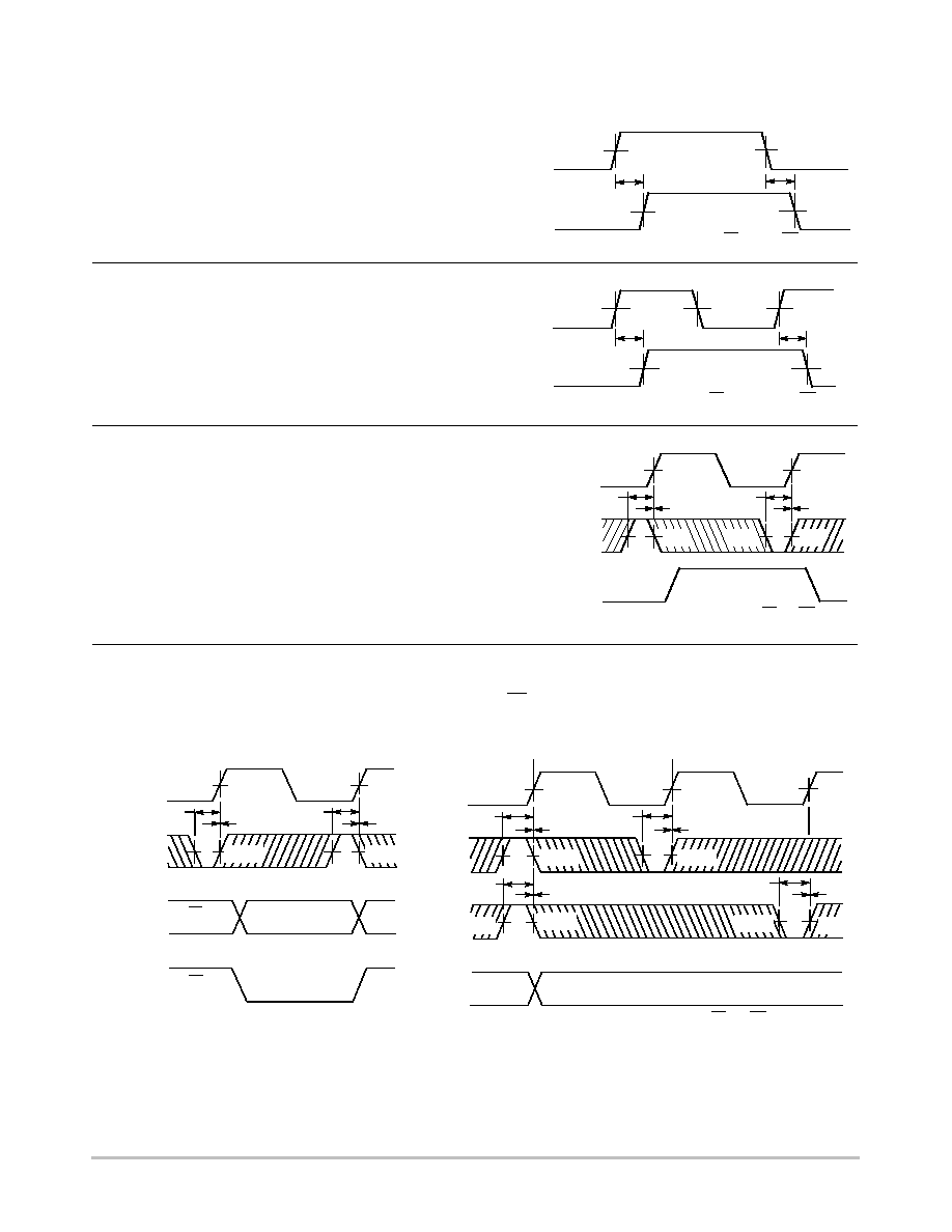
AC WAVEFORMS
Figure 1. Clock to Output Delays, Count
Frequency, and Clock Pulse Width
Figure 2. Master Reset to Output Delay, Master Reset
Pulse Width, and Master Reset Recovery Time
1.3 V
1.3 V
1.3 V
1.3 V
1.3 V
1.3 V
1.3 V
CP
Q
tW(H)
tW(L)
trec
tPHL
tPHL
tPLH
Other conditions:
PE = MR (SR) = H
CEP = CET = H
Other conditions:
PE = L
P
0
= P
1
= P
2
= P
3
= H
tW
Q
0
V
Q
1
V
Q
2
V
Q
3
MR
CP
SN74LS161A, SN74LS163A
http://onsemi.com
6
Figure 3.
The positive TC pulse occurs when the outputs are in the (Q0
∑
Q1
∑
Q2
∑
Q3) state for the LS161 and LS163.
OTHER CONDITIONS: CP = PE = CEP = MR = H
1.3 V
tPHL
tPLH
1.3 V
1.3 V
1.3 V
CET
TC
AC WAVEFORMS (continued)
The positive TC pulse is coincident with the output state
(Q0
∑
Q1
∑
Q2
∑
Q3) for the LS161 and LS163.
Figure 4.
OTHER CONDITIONS: PE = CEP = CET = MR = H
1.3 V
1.3 V
1.3 V
1.3 V
1.3 V
tPLH
tPHL
CP
TC
The shaded areas indicate when the input is permitted to
change for predictable output performance.
Figure 5.
1.3 V
1.3 V
OTHER CONDITIONS: PE = L, MR = H
CP
1.3 V
1.3 V
1.3 V
ts(H)
ts(L)
th(H) = 0
th(L) = 0
Q
0
w
Q
1
w
Q
2
w
Q
3
P
0
w
P
1
w
P
2
w
P
3
OTHER CONDITIONS: PE = H, MR = H
1.3 V
1.3 V
1.3 V
1.3 V
1.3 V
1.3 V
1.3 V
1.3 V
1.3 V
1.3 V
1.3 V
ts(H)
ts(L)
th(H) = 0
th(L) = 0
ts(H)
th(H) = 0
ts(L)
th(L) = 0
COUNT
HOLD
HOLD
CEP
CP
CET
Q
CP
SR or PE
Q RESPONSE TO PE
RESET
COUNT OR LOAD
Q RESPONSE TO SR
PARALLEL LOAD
(See Fig. 5)
COUNT MODE
(See Fig. 7)
ts(L)
ts(H)
th
(L) = 0
th(H) = 0
1.3 V
1.3 V
Figure 6.
COUNT ENABLE TRICKLE INPUT
TO TERMINAL COUNT OUTPUT DELAYS
CLOCK TO TERMINAL COUNT DELAYS
SETUP TIME (ts) AND HOLD TIME (th)
FOR PARALLEL DATA INPUTS
SETUP TIME (ts) AND HOLD TIME (th) FOR
COUNT ENABLE (CEP) AND (CET) AND
PARALLEL ENABLE (PE) INPUTS
Figure 7.
The shaded areas indicate when the input is permitted to
change for predictable output performance.
1.3 V
SN74LS161A, SN74LS163A
http://onsemi.com
7
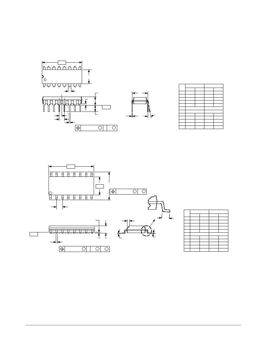
PACKAGE DIMENSIONS
N SUFFIX
PLASTIC PACKAGE
CASE 648≠08
ISSUE R
NOTES:
1. DIMENSIONING AND TOLERANCING PER ANSI
Y14.5M, 1982.
2. CONTROLLING DIMENSION: INCH.
3. DIMENSION L TO CENTER OF LEADS WHEN
FORMED PARALLEL.
4. DIMENSION B DOES NOT INCLUDE MOLD FLASH.
5. ROUNDED CORNERS OPTIONAL.
≠A≠
B
F
C
S
H
G
D
J
L
M
16 PL
SEATING
1
8
9
16
K
PLANE
≠T≠
M
A
M
0.25 (0.010)
T
DIM
MIN
MAX
MIN
MAX
MILLIMETERS
INCHES
A
0.740
0.770
18.80
19.55
B
0.250
0.270
6.35
6.85
C
0.145
0.175
3.69
4.44
D
0.015
0.021
0.39
0.53
F
0.040
0.70
1.02
1.77
G
0.100 BSC
2.54 BSC
H
0.050 BSC
1.27 BSC
J
0.008
0.015
0.21
0.38
K
0.110
0.130
2.80
3.30
L
0.295
0.305
7.50
7.74
M
0
10
0
10
S
0.020
0.040
0.51
1.01
_
_
_
_
D SUFFIX
PLASTIC SOIC PACKAGE
CASE 751B≠05
ISSUE J
NOTES:
1. DIMENSIONING AND TOLERANCING PER ANSI
Y14.5M, 1982.
2. CONTROLLING DIMENSION: MILLIMETER.
3. DIMENSIONS A AND B DO NOT INCLUDE
MOLD PROTRUSION.
4. MAXIMUM MOLD PROTRUSION 0.15 (0.006)
PER SIDE.
5. DIMENSION D DOES NOT INCLUDE DAMBAR
PROTRUSION. ALLOWABLE DAMBAR
PROTRUSION SHALL BE 0.127 (0.005) TOTAL
IN EXCESS OF THE D DIMENSION AT
MAXIMUM MATERIAL CONDITION.
1
8
16
9
SEATING
PLANE
F
J
M
R
X 45
_
G
8 PL
P
≠B≠
≠A≠
M
0.25 (0.010)
B
S
≠T≠
D
K
C
16 PL
S
B
M
0.25 (0.010)
A
S
T
DIM
MIN
MAX
MIN
MAX
INCHES
MILLIMETERS
A
9.80
10.00
0.386
0.393
B
3.80
4.00
0.150
0.157
C
1.35
1.75
0.054
0.068
D
0.35
0.49
0.014
0.019
F
0.40
1.25
0.016
0.049
G
1.27 BSC
0.050 BSC
J
0.19
0.25
0.008
0.009
K
0.10
0.25
0.004
0.009
M
0
7
0
7
P
5.80
6.20
0.229
0.244
R
0.25
0.50
0.010
0.019
_
_
_
_
SN74LS161A, SN74LS163A
http://onsemi.com
8
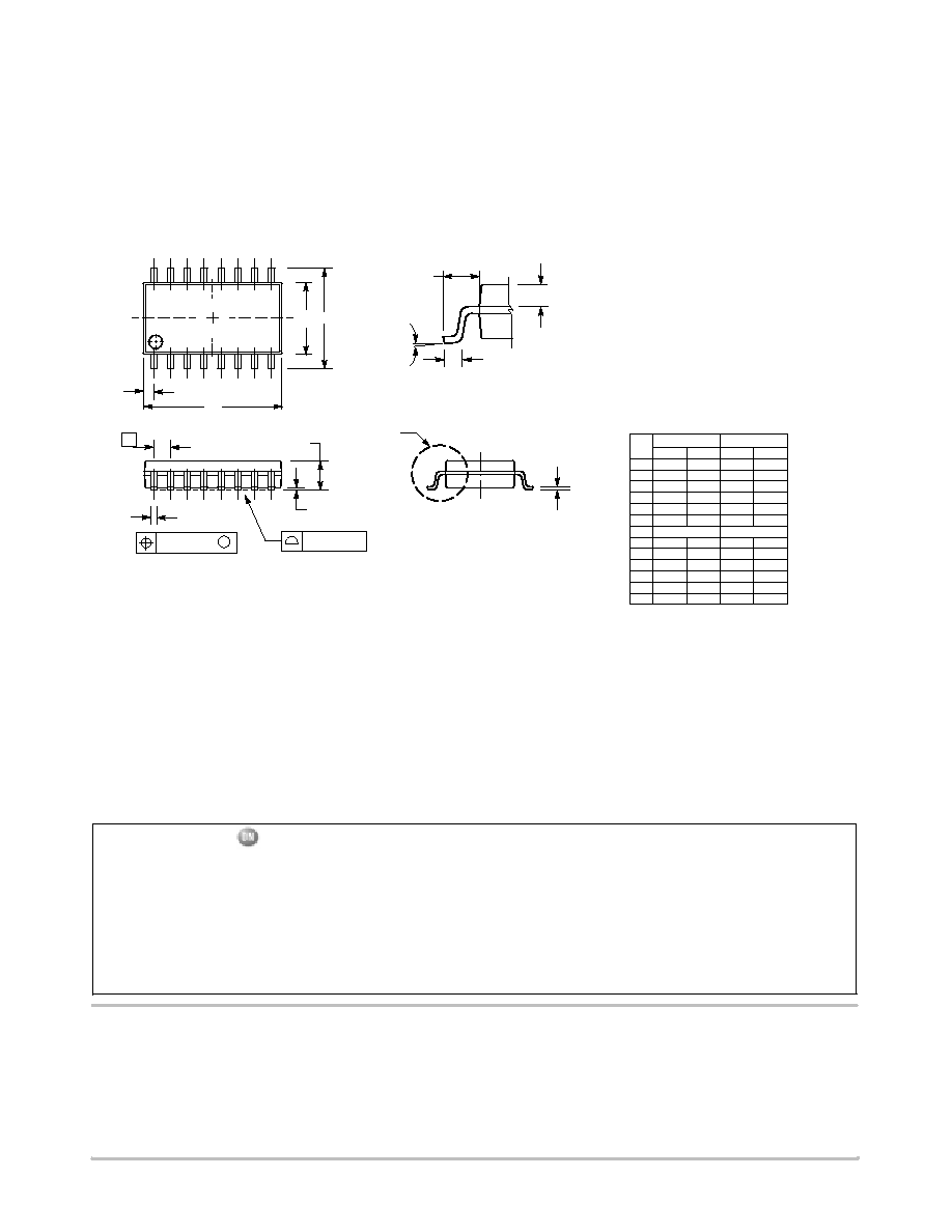
PACKAGE DIMENSIONS
HE
A1
DIM
MIN
MAX
MIN
MAX
INCHES
---
2.05
---
0.081
MILLIMETERS
0.05
0.20
0.002
0.008
0.35
0.50
0.014
0.020
0.18
0.27
0.007
0.011
9.90
10.50
0.390
0.413
5.10
5.45
0.201
0.215
1.27 BSC
0.050 BSC
7.40
8.20
0.291
0.323
0.50
0.85
0.020
0.033
1.10
1.50
0.043
0.059
0
0.70
0.90
0.028
0.035
---
0.78
---
0.031
A1
HE
Q1
LE
_
10
_
0
_
10
_
LE
Q1
_
NOTES:
1. DIMENSIONING AND TOLERANCING PER ANSI
Y14.5M, 1982.
2. CONTROLLING DIMENSION: MILLIMETER.
3. DIMENSIONS D AND E DO NOT INCLUDE MOLD
FLASH OR PROTRUSIONS AND ARE MEASURED
AT THE PARTING LINE. MOLD FLASH OR
PROTRUSIONS SHALL NOT EXCEED 0.15 (0.006)
PER SIDE.
4. TERMINAL NUMBERS ARE SHOWN FOR
REFERENCE ONLY.
5. THE LEAD WIDTH DIMENSION (b) DOES NOT
INCLUDE DAMBAR PROTRUSION. ALLOWABLE
DAMBAR PROTRUSION SHALL BE 0.08 (0.003)
TOTAL IN EXCESS OF THE LEAD WIDTH
DIMENSION AT MAXIMUM MATERIAL CONDITION.
DAMBAR CANNOT BE LOCATED ON THE LOWER
RADIUS OR THE FOOT. MINIMUM SPACE
BETWEEN PROTRUSIONS AND ADJACENT LEAD
TO BE 0.46 ( 0.018).
M
L
DETAIL P
VIEW P
c
A
b
e
M
0.13 (0.005)
0.10 (0.004)
1
16
9
8
D
Z
E
A
b
c
D
E
e
L
M
Z
M SUFFIX
SOEIAJ PACKAGE
CASE 966≠01
ISSUE O
ON Semiconductor and are trademarks of Semiconductor Components Industries, LLC (SCILLC). SCILLC reserves the right to make changes
without further notice to any products herein. SCILLC makes no warranty, representation or guarantee regarding the suitability of its products for any particular
purpose, nor does SCILLC assume any liability arising out of the application or use of any product or circuit, and specifically disclaims any and all liability,
including without limitation special, consequential or incidental damages. "Typical" parameters which may be provided in SCILLC data sheets and/or
specifications can and do vary in different applications and actual performance may vary over time. All operating parameters, including "Typicals" must be
validated for each customer application by customer's technical experts. SCILLC does not convey any license under its patent rights nor the rights of others.
SCILLC products are not designed, intended, or authorized for use as components in systems intended for surgical implant into the body, or other applications
intended to support or sustain life, or for any other application in which the failure of the SCILLC product could create a situation where personal injury or
death may occur. Should Buyer purchase or use SCILLC products for any such unintended or unauthorized application, Buyer shall indemnify and hold
SCILLC and its officers, employees, subsidiaries, affiliates, and distributors harmless against all claims, costs, damages, and expenses, and reasonable
attorney fees arising out of, directly or indirectly, any claim of personal injury or death associated with such unintended or unauthorized use, even if such claim
alleges that SCILLC was negligent regarding the design or manufacture of the part. SCILLC is an Equal Opportunity/Affirmative Action Employer.
PUBLICATION ORDERING INFORMATION
JAPAN: ON Semiconductor, Japan Customer Focus Center
4≠32≠1 Nishi≠Gotanda, Shinagawa≠ku, Tokyo, Japan 141≠0031
Phone: 81≠3≠5740≠2700
Email: r14525@onsemi.com
ON Semiconductor Website: http://onsemi.com
For additional information, please contact your local
Sales Representative.
SN74LS161A/D
Literature Fulfillment:
Literature Distribution Center for ON Semiconductor
P.O. Box 5163, Denver, Colorado 80217 USA
Phone: 303≠675≠2175 or 800≠344≠3860 Toll Free USA/Canada
Fax: 303≠675≠2176 or 800≠344≠3867 Toll Free USA/Canada
Email: ONlit@hibbertco.com
N. American Technical Support: 800≠282≠9855 Toll Free USA/Canada