©
Semiconductor Components Industries, LLC, 2001
October, 2001 ≠ Rev. 7
1
Publication Order Number:
SN74LS165/D
SN74LS165
8-Bit Parallel-to-Serial
Shift Register
The SN74LS165 is an 8-bit parallel load or serial-in register with
complementary outputs available from the last stage. Parallel inputing
occurs asynchronously when the Parallel Load (PL) input is LOW.
With PL HIGH, serial shifting occurs on the rising edge of the clock;
new data enters via the Serial Data (DS) input. The 2-input OR clock
can be used to combine two independent clock sources, or one input
can act as an active LOW clock enable.
GUARANTEED OPERATING RANGES
Symbol
Parameter
Min
Typ
Max
Unit
VCC
Supply Voltage
4.75
5.0
5.25
V
TA
Operating Ambient
Temperature Range
0
25
70
∞
C
IOH
Output Current ≠ High
≠0.4
mA
IOL
Output Current ≠ Low
8.0
mA
LOW
POWER
SCHOTTKY
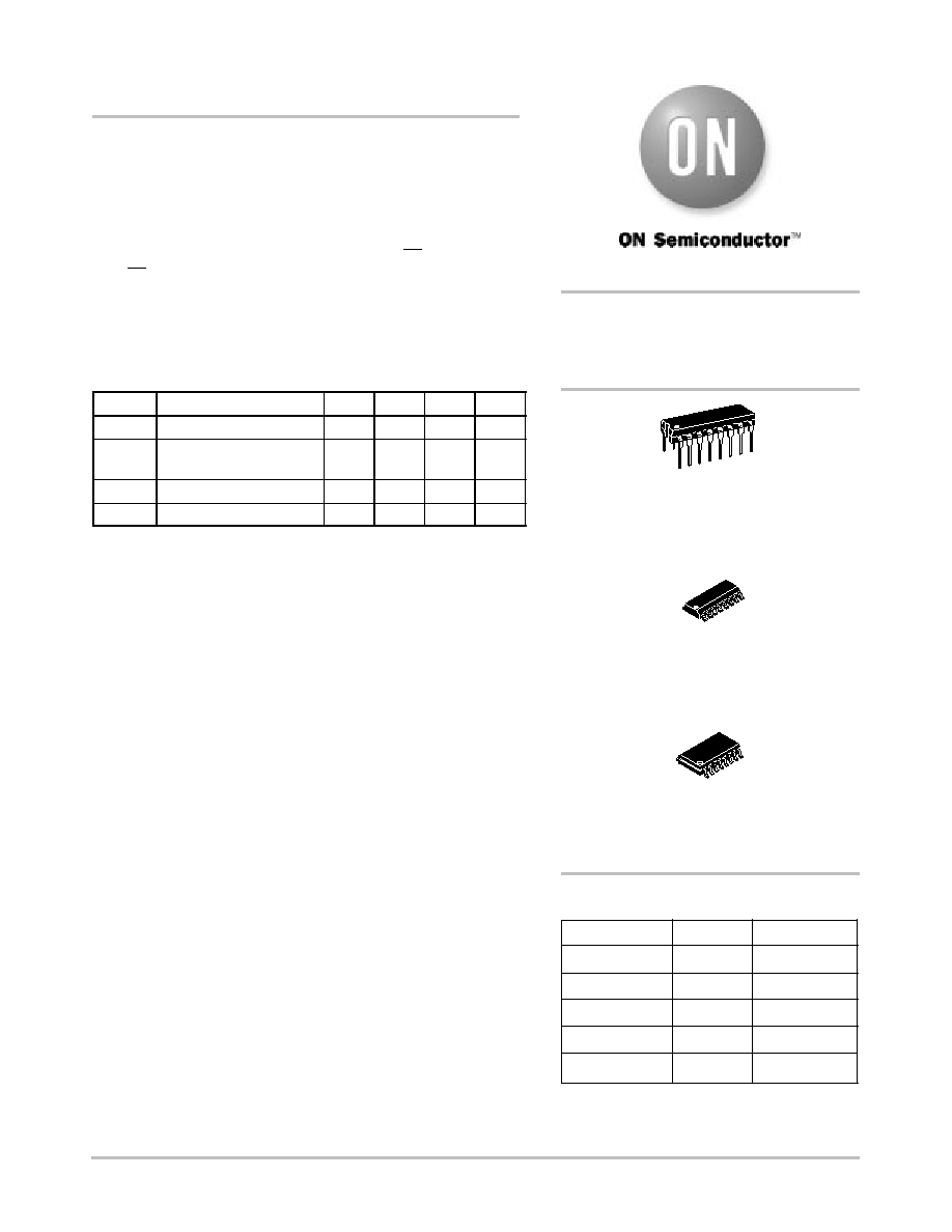
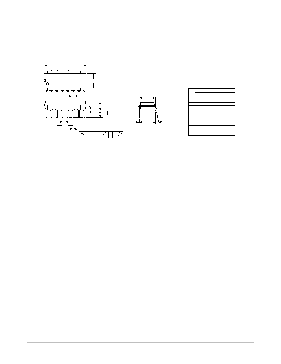
SOIC
D SUFFIX
CASE 751B
PLASTIC
N SUFFIX
CASE 648
16
1
16
1
SOEIAJ
M SUFFIX
CASE 966
16
1
Device
Package
Shipping
ORDERING INFORMATION
SN74LS165N
16 Pin DIP
2000 Units/Box
SN74LS165D
SOIC≠16
38 Units/Rail
SN74LS165DR2
SOIC≠16
2500/Tape & Reel
SN74LS165M
SOEIAJ≠16
See Note 1
SN74LS165MEL
SOEIAJ≠16
1. For ordering information on the EIAJ version of
the SOIC package, please contact your local
ON Semiconductor representative.
See Note 1
http://onsemi.com
SN74LS165
http://onsemi.com
2
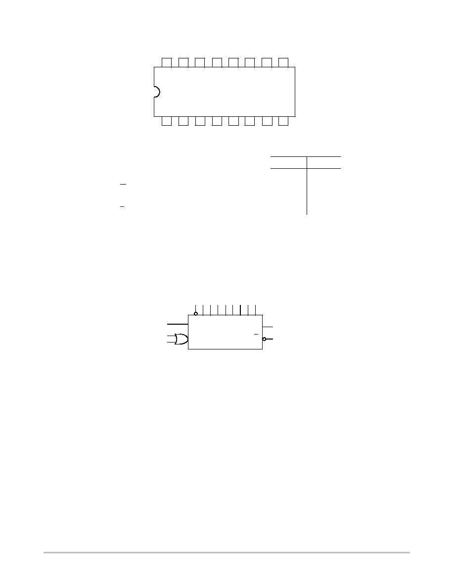
CONNECTION DIAGRAM DIP (TOP VIEW)
Clock (LOW-to-HIGH Going Edge) Inputs
Serial Data Input
Asynchronous Parallel Load (Active LOW) Input
Parallel Data Inputs
Serial Output from Last State
Complementary Output
CP1, CP2
DS
PL
P0 - P7
Q7
Q7
0.5 U.L.
0.5 U.L.
1.5 U.L.
0.5 U.L.
10 U.L.
10 U.L.
0.25 U.L.
0.25 U.L.
0.75 U.L.
0.25 U.L.
5 U.L.
5 U.L.
NOTES:
a) 1 TTL Unit Load (U.L.) = 40 mA HIGH/1.6 mA LOW.
HIGH
LOW
(Note a)
LOADING
PIN NAMES
VCC = PIN 16
GND = PIN 8
LOGIC SYMBOL
NOTE:
The Flatpak version has the same
pinouts (Connection Diagram) as
the Dual In Line Package.
1 11 12 13 14 3 4 5 6
9
7
10
2
15
DS
CP
Q7
Q7
PL P0P1 P2 P3P4 P5P6 P7
14
13
12
11
10
9
1
2
3
4
5
6
7
16
15
8
VCC
PL
CP2 P3
P2
P1
DS
P0
Q7
CP1 P4
P5
P6
P7
Q7 GND
SN74LS165
http://onsemi.com
3
LOGIC DIAGRAM
PL
CP1
P4
P6
P5
P7
CP2
P3
P1
P2
P0
DS
PRESET
S
CP
R CL
Q0
Q0
PRESET
S
CP
R CL
Q1
Q1
PRESET
S
CP
R CL
Q2
Q2
PRESET
S
CP
R CL
Q3
Q3
PRESET
S
CP
R CL
Q4
Q4
PRESET
S
CP
R CL
Q5
Q5
PRESET
S
CP
R CL
Q6
Q6
PRESET
S
CP
R CL
Q7
Q7
14
1
2
6
3
4
5
11
12
10
13
15
VCC = PIN 16
GND = PIN 8
= PIN NUMBERS
7
9
FUNCTIONAL DESCRIPTION
The SN74LS165 contains eight clocked master/slave RS
flip-flops connected as a shift register, with auxiliary gating
to provide overriding asynchronous parallel entry. Parallel
data enters when the PL signal is LOW. The parallel data can
change while PL is LOW, provided that the recommended
setup and hold times are observed.
For clock operation, PL must be HIGH. The two clock
inputs perform identically; one can be used as a clock inhibit
by applying a HIGH signal. To avoid double clocking,
however, the inhibit signal should only go HIGH while the
clock is HIGH. Otherwise, the rising inhibit signal will cause
the same response as a rising clock edge. The flip-flops are
edge-triggered for serial operations. The serial input data
can change at any time, provided only that the recommended
setup and hold times are observed, with respect to the rising
edge of the clock.
TRUTH TABLE
PL
CP
CONTENTS
RESPONSE
PL
1
2
Q0
Q1
Q2
Q3
Q4
Q5
Q6
Q7
RESPONSE
L
X
X
P0
P1
P2
P3
P4
P5
P6
P7
Parallel Entry
H
L
DS
Q0
Q1
Q2
Q3
Q4
Q5
Q6
Right Shift
H
H
Q0
Q1
Q2
Q3
Q4
Q5
Q6
Q7
No Change
H
L
DS
Q0
Q1
Q2
Q3
Q4
Q5
Q6
Right Shift
H
H
Q0
Q1
Q2
Q3
Q4
Q5
Q6
Q7
No Change
H = HIGH Voltage Level
L = LOW Voltage Level
X = Immaterial

SN74LS165
http://onsemi.com
4
DC CHARACTERISTICS OVER OPERATING TEMPERATURE RANGE
(unless otherwise specified)
Limits
Symbol
Parameter
Min
Typ
Max
Unit
Test Conditions
VIH
Input HIGH Voltage
2.0
V
Guaranteed Input HIGH Voltage for
All Inputs
VIL
Input LOW Voltage
0.8
V
Guaranteed Input LOW Voltage for
All Inputs
VIK
Input Clamp Diode Voltage
≠0.65
≠1.5
V
VCC = MIN, IIN = ≠18 mA
VOH
Output HIGH Voltage
2.7
3.5
V
VCC = MIN, IOH = MAX, VIN = VIH
or VIL per Truth Table
VOL
Output LOW Voltage
0.25
0.4
V
IOL = 4.0 mA
VCC = VCC MIN,
VIN VIL or VIH
VOL
Output LOW Voltage
0.35
0.5
V
IOL = 8.0 mA
VIN = VIL or VIH
per Truth Table
IIH
Input HIGH Current
Other Inputs
PL Input
20
60
µ
A
VCC = MAX, VIN = 2.7 V
IIH
Other Inputs
PL Input
0.1
0.3
mA
VCC = MAX, VIN = 7.0 V
IIL
Input LOW Current
Other Inputs
PL Input
≠0.4
≠1.2
mA
VCC = MAX, VIN = 0.4 V
IOS
Short Circuit Current (Note 2)
≠20
≠100
mA
VCC = MAX
ICC
Power Supply Current
36
mA
VCC = MAX
2. Not more than one output should be shorted at a time, nor for more than 1 second.
AC CHARACTERISTICS
(TA = 25
∞
C)
Limits
Symbol
Parameter
Min
Typ
Max
Unit
Test Conditions
fMAX
Maximum Input Clock Frequency
25
35
MHz
tPLH
tPHL
Propagation Delay
PL to Output
22
22
35
35
ns
tPLH
tPHL
Propagation Delay
Clock to Output
27
28
40
40
ns
VCC = 5.0 V
CL = 15 pF
tPLH
tPHL
Propagation Delay
P7 to Q7
14
21
25
30
ns
CL = 15 pF
tPLH
tPHL
Propagation Delay
P7 to Q7
21
16
30
25
ns
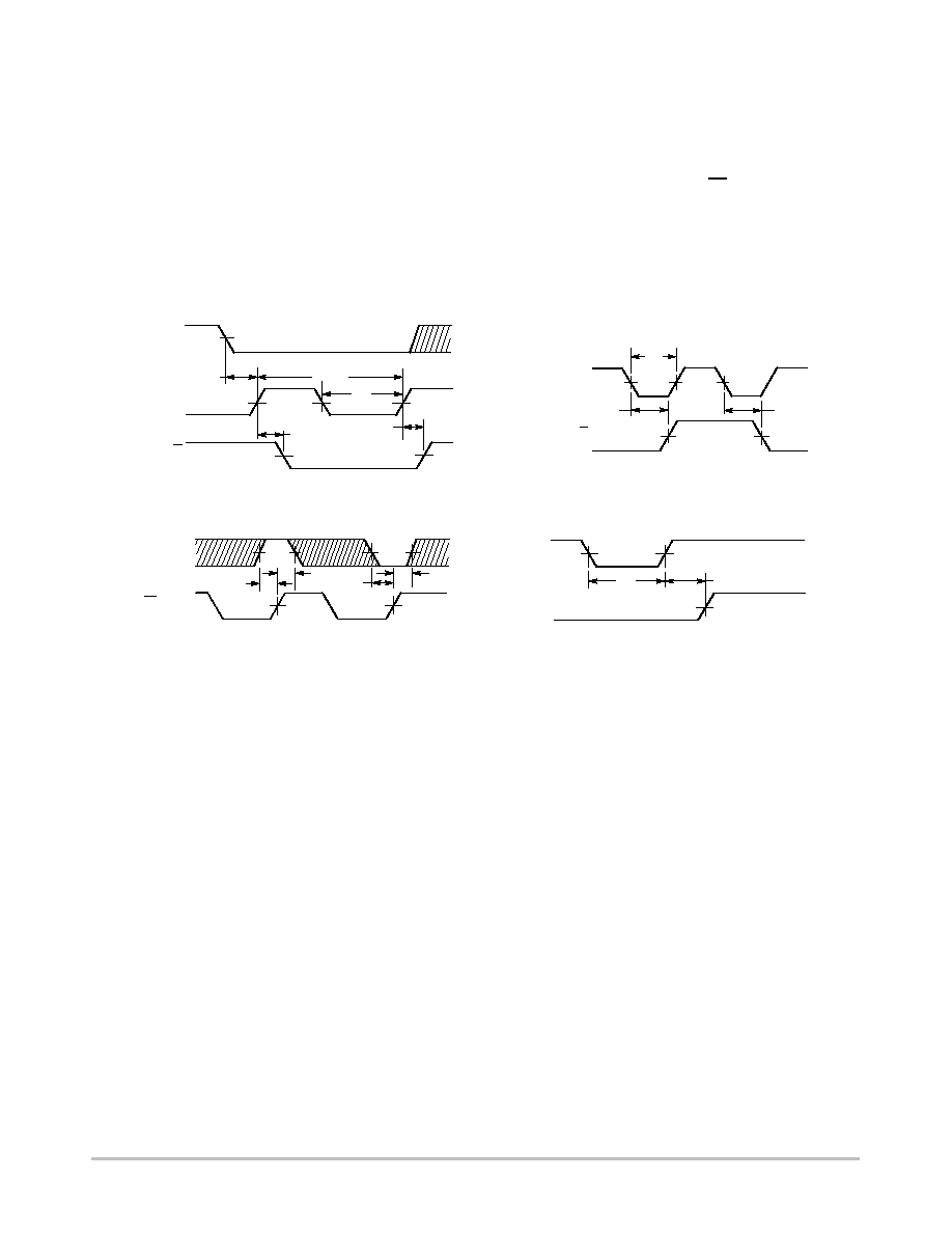
AC SETUP REQUIREMENTS
(TA = 25
∞
C)
Limits
Symbol
Parameter
Min
Typ
Max
Unit
Test Conditions
tW
CP Clock Pulse Width
25
ns
tW
PL Pulse Width
15
ns
ts
Parallel Data Setup Time
10
ns
ts
Serial Data Setup Time
20
ns
VCC = 5.0 V
ts
CP1 to CP2 Setup Time1
30
ns
CC
th
Hold Time
0
ns
trec
Recovery Time, PL to CP
45
ns
1The role of CP1 and CP2 in an application may be interchanged.
SN74LS165
http://onsemi.com
5
DEFINITION OF TERMS:
SETUP TIME (ts) -- is defined as the minimum time
required for the correct logic level to be present at the logic
input prior to the clock transition from LOW-to-HIGH in
order to be recognized and transferred to the outputs.
HOLD TIME (th) -- is defined as the minimum time
following the clock transition from LOW-to-HIGH that the
logic level must be maintained at the input in order to ensure
continued recognition. A negative hold time indicates that
the correct logic level may be released prior to the clock
transition from LOW-to-HIGH and still be recognized.
RECOVERY TIME (trec) -- is defined as the minimum time
required between the end of the PL pulse and the clock
transition from LOW-to-HIGH in order to recognize and
transfer loaded Data to the Q outputs.
AC WAVEFORMS
tW
1.3 V
1.3 V
1.3 V
1.3 V
1.3 V
1.3 V
1.3 V
1.3 V
1.3 V
1.3 V
1.3 V
1.3 V
1.3 V
1.3 V
1.3 V
CP1
CP2
Q7 OR Q7
Pn
PL OR CP
tPHL
tPLH
PL
CP
trec
Q7 OR Q7
PL
tPHL
tPLH
tW
tW
1/fmax
ts
ts(H)
th(H) ts(L)
th(L)
Figure 1.
Figure 2.
1.3 V
Figure 3.
Figure 4.
SN74LS165
http://onsemi.com
6
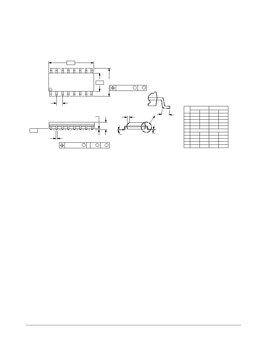
PACKAGE DIMENSIONS
N SUFFIX
PLASTIC PACKAGE
CASE 648≠08
ISSUE R
NOTES:
1. DIMENSIONING AND TOLERANCING PER ANSI
Y14.5M, 1982.
2. CONTROLLING DIMENSION: INCH.
3. DIMENSION L TO CENTER OF LEADS WHEN
FORMED PARALLEL.
4. DIMENSION B DOES NOT INCLUDE MOLD FLASH.
5. ROUNDED CORNERS OPTIONAL.
≠A≠
B
F
C
S
H
G
D
J
L
M
16 PL
SEATING
1
8
9
16
K
PLANE
≠T≠
M
A
M
0.25 (0.010)
T
DIM
MIN
MAX
MIN
MAX
MILLIMETERS
INCHES
A
0.740
0.770
18.80
19.55
B
0.250
0.270
6.35
6.85
C
0.145
0.175
3.69
4.44
D
0.015
0.021
0.39
0.53
F
0.040
0.70
1.02
1.77
G
0.100 BSC
2.54 BSC
H
0.050 BSC
1.27 BSC
J
0.008
0.015
0.21
0.38
K
0.110
0.130
2.80
3.30
L
0.295
0.305
7.50
7.74
M
0
10
0
10
S
0.020
0.040
0.51
1.01
_
_
_
_
SN74LS165
http://onsemi.com
7
PACKAGE DIMENSIONS
D SUFFIX
PLASTIC SOIC PACKAGE
CASE 751B≠05
ISSUE J
NOTES:
1. DIMENSIONING AND TOLERANCING PER ANSI
Y14.5M, 1982.
2. CONTROLLING DIMENSION: MILLIMETER.
3. DIMENSIONS A AND B DO NOT INCLUDE
MOLD PROTRUSION.
4. MAXIMUM MOLD PROTRUSION 0.15 (0.006)
PER SIDE.
5. DIMENSION D DOES NOT INCLUDE DAMBAR
PROTRUSION. ALLOWABLE DAMBAR
PROTRUSION SHALL BE 0.127 (0.005) TOTAL
IN EXCESS OF THE D DIMENSION AT
MAXIMUM MATERIAL CONDITION.
1
8
16
9
SEATING
PLANE
F
J
M
R
X 45
_
G
8 PL
P
≠B≠
≠A≠
M
0.25 (0.010)
B
S
≠T≠
D
K
C
16 PL
S
B
M
0.25 (0.010)
A
S
T
DIM
MIN
MAX
MIN
MAX
INCHES
MILLIMETERS
A
9.80
10.00
0.386
0.393
B
3.80
4.00
0.150
0.157
C
1.35
1.75
0.054
0.068
D
0.35
0.49
0.014
0.019
F
0.40
1.25
0.016
0.049
G
1.27 BSC
0.050 BSC
J
0.19
0.25
0.008
0.009
K
0.10
0.25
0.004
0.009
M
0
7
0
7
P
5.80
6.20
0.229
0.244
R
0.25
0.50
0.010
0.019
_
_
_
_
SN74LS165
http://onsemi.com
8
PACKAGE DIMENSIONS
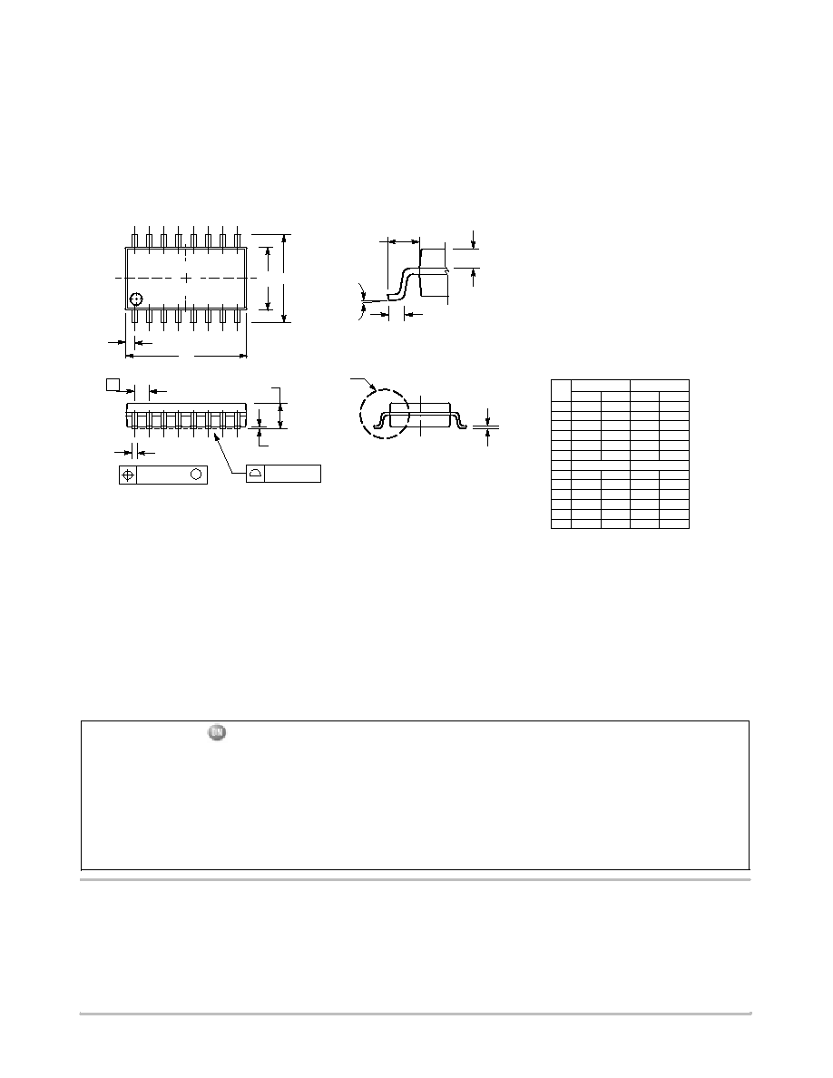
HE
A1
DIM
MIN
MAX
MIN
MAX
INCHES
---
2.05
---
0.081
MILLIMETERS
0.05
0.20
0.002
0.008
0.35
0.50
0.014
0.020
0.18
0.27
0.007
0.011
9.90
10.50
0.390
0.413
5.10
5.45
0.201
0.215
1.27 BSC
0.050 BSC
7.40
8.20
0.291
0.323
0.50
0.85
0.020
0.033
1.10
1.50
0.043
0.059
0
0.70
0.90
0.028
0.035
---
0.78
---
0.031
A1
HE
Q1
LE
_
10
_
0
_
10
_
LE
Q1
_
NOTES:
1. DIMENSIONING AND TOLERANCING PER ANSI
Y14.5M, 1982.
2. CONTROLLING DIMENSION: MILLIMETER.
3. DIMENSIONS D AND E DO NOT INCLUDE MOLD
FLASH OR PROTRUSIONS AND ARE MEASURED
AT THE PARTING LINE. MOLD FLASH OR
PROTRUSIONS SHALL NOT EXCEED 0.15 (0.006)
PER SIDE.
4. TERMINAL NUMBERS ARE SHOWN FOR
REFERENCE ONLY.
5. THE LEAD WIDTH DIMENSION (b) DOES NOT
INCLUDE DAMBAR PROTRUSION. ALLOWABLE
DAMBAR PROTRUSION SHALL BE 0.08 (0.003)
TOTAL IN EXCESS OF THE LEAD WIDTH
DIMENSION AT MAXIMUM MATERIAL CONDITION.
DAMBAR CANNOT BE LOCATED ON THE LOWER
RADIUS OR THE FOOT. MINIMUM SPACE
BETWEEN PROTRUSIONS AND ADJACENT LEAD
TO BE 0.46 ( 0.018).
M
L
DETAIL P
VIEW P
c
A
b
e
M
0.13 (0.005)
0.10 (0.004)
1
16
9
8
D
Z
E
A
b
c
D
E
e
L
M
Z
M SUFFIX
SOEIAJ PACKAGE
CASE 966≠01
ISSUE O
ON Semiconductor and are trademarks of Semiconductor Components Industries, LLC (SCILLC). SCILLC reserves the right to make changes
without further notice to any products herein. SCILLC makes no warranty, representation or guarantee regarding the suitability of its products for any particular
purpose, nor does SCILLC assume any liability arising out of the application or use of any product or circuit, and specifically disclaims any and all liability,
including without limitation special, consequential or incidental damages. "Typical" parameters which may be provided in SCILLC data sheets and/or
specifications can and do vary in different applications and actual performance may vary over time. All operating parameters, including "Typicals" must be
validated for each customer application by customer's technical experts. SCILLC does not convey any license under its patent rights nor the rights of others.
SCILLC products are not designed, intended, or authorized for use as components in systems intended for surgical implant into the body, or other applications
intended to support or sustain life, or for any other application in which the failure of the SCILLC product could create a situation where personal injury or
death may occur. Should Buyer purchase or use SCILLC products for any such unintended or unauthorized application, Buyer shall indemnify and hold
SCILLC and its officers, employees, subsidiaries, affiliates, and distributors harmless against all claims, costs, damages, and expenses, and reasonable
attorney fees arising out of, directly or indirectly, any claim of personal injury or death associated with such unintended or unauthorized use, even if such claim
alleges that SCILLC was negligent regarding the design or manufacture of the part. SCILLC is an Equal Opportunity/Affirmative Action Employer.
PUBLICATION ORDERING INFORMATION
JAPAN: ON Semiconductor, Japan Customer Focus Center
4≠32≠1 Nishi≠Gotanda, Shinagawa≠ku, Tokyo, Japan 141≠0031
Phone: 81≠3≠5740≠2700
Email: r14525@onsemi.com
ON Semiconductor Website: http://onsemi.com
For additional information, please contact your local
Sales Representative.
SN74LS165/D
Literature Fulfillment:
Literature Distribution Center for ON Semiconductor
P.O. Box 5163, Denver, Colorado 80217 USA
Phone: 303≠675≠2175 or 800≠344≠3860 Toll Free USA/Canada
Fax: 303≠675≠2176 or 800≠344≠3867 Toll Free USA/Canada
Email: ONlit@hibbertco.com
N. American Technical Support: 800≠282≠9855 Toll Free USA/Canada