©
Semiconductor Components Industries, LLC, 1999
December, 1999 ≠ Rev. 6
1
Publication Order Number:
SN74LS377/D
SN74LS377
Octal D Flip-Flop
with Enable
The SN74LS377 is an 8-bit register built using advanced Low
Power Schottky technology. This register consists of eight D-type
flip-flops with a buffered common clock and a buffered common
clock enable.
∑
8-Bit High Speed Parallel Registers
∑
Positive Edge-Triggered D-Type Flip Flops
∑
Fully Buffered Common Clock and Enable Inputs
∑
True and Complement Outputs
∑
Input Clamp Diodes Limit High Speed Termination Effects
GUARANTEED OPERATING RANGES
Symbol
Parameter
Min
Typ
Max
Unit
V
CC
Supply Voltage
4.75
5.0
5.25
V
T
A
Operating Ambient
Temperature Range
0
25
70
∞
C
I
OH
Output Current ≠ High
≠ 0.4
mA
I
OL
Output Current ≠ Low
8.0
mA
LOW
POWER
SCHOTTKY
Device
Package
Shipping
ORDERING INFORMATION
SN74LS377N
16 Pin DIP
1440 Units/Box
SN74LS377DW
16 Pin
SOIC
DW SUFFIX
CASE 751D
http://onsemi.com
2500/Tape & Reel
PLASTIC
N SUFFIX
CASE 738
20
1
20
1

SN74LS377
http://onsemi.com
2
CONNECTION DIAGRAM DIP (TOP VIEW)
Enable (Active LOW) Input
Data Inputs
Clock (Active HIGH Going Edge) Input
True Outputs
Complemented Outputs
E
D
0
≠ D
3
CP
Q
0
≠ Q
3
Q
0
≠ Q
3
0.5 U.L.
0.5 U.L.
0.5 U.L.
10 U.L.
10 U.L.
0.25 U.L.
0.25 U.L.
0.25 U.L.
5 U.L.
5 U.L.
NOTES:
a) 1 TTL Unit Load (U.L.) = 40
mA HIGH/1.6 mA LOW.
HIGH
LOW
(Note a)
LOADING
PIN NAMES
NOTE:
The Flatpak version
has the same pinouts
(Connection Diagram) as
the Dual In-Line Package.
18
17
16
15
14
13
1
2
3
4
5
6
7
20
19
8
V
CC
E
Q
7
D
7
D
6
Q
6
D
5
Q
5
D
4
Q
0
D
0
D
1
Q
1
Q
2
D
2
D
3
9
10
Q
3
GND
12
11
Q
4
CP
LOGIC DIAGRAM
E
ENABLE
D
0
D
1
D
2
D
3
D
4
D
5
D
6
D
7
Q
0
Q
1
Q
2
Q
3
Q
4
Q
5
Q
6
Q
7
CP
CLOCK
CP D
Q
14
2
6
7
3
8
4
5
9
12
16
13
17
CP D
Q
CP D
Q
CP D
Q
CP D
Q
CP D
Q
CP D
Q
CP D
Q
18
15
19
1
11
SN74LS377
http://onsemi.com
3
DC CHARACTERISTICS OVER OPERATING TEMPERATURE RANGE
(unless otherwise specified)
Limits
Symbol
Parameter
Min
Typ
Max
Unit
Test Conditions
V
IH
Input HIGH Voltage
2.0
V
Guaranteed Input HIGH Voltage for
All Inputs
V
IL
Input LOW Voltage
0.8
V
Guaranteed Input LOW Voltage for
All Inputs
V
IK
Input Clamp Diode Voltage
≠ 0.65
≠ 1.5
V
V
CC
= MIN, I
IN
= ≠ 18 mA
V
OH
Output HIGH Voltage
2.7
3.5
V
V
CC
= MIN, I
OH
= MAX, V
IN
= V
IH
or V
IL
per Truth Table
V
O
Output LOW Voltage
0.25
0.4
V
I
OL
= 4.0 mA
V
CC
= V
CC
MIN,
V
V
or V
V
OL
Output LOW Voltage
0.35
0.5
V
I
OL
= 8.0 mA
V
IN
= V
IL
or V
IH
per Truth Table
I
Input HIGH Current
20
µ
A
V
CC
= MAX, V
IN
= 2.7 V
I
IH
Input HIGH Current
0.1
mA
V
CC
= MAX, V
IN
= 7.0 V
I
IL
Input LOW Current
≠ 0.4
mA
V
CC
= MAX, V
IN
= 0.4 V
I
OS
Short Circuit Current (Note 1)
≠ 20
≠ 100
mA
V
CC
= MAX
I
CC
Power Supply Current
28
mA
V
CC
= MAX, NOTE 1
NOTE: With all inputs open and GND applied to all data and enable inputs, I
CC
is measured after a momentary GND, then 4.5 V is applied to clock.
Note 1: Not more than one output should be shorted at a time, nor for more than 1 second.
AC CHARACTERISTICS
(T
A
= 25
∞
C, V
CC
= 5.0 V)
Limits
Symbol
Parameter
Min
Typ
Max
Unit
Test Conditions
f
MAX
Maximum Clock Frequency
30
40
MHz
V
CC
= 5 0 V
t
PLH
t
PHL
Propagation Delay,
Clock to Output
17
18
27
27
ns
V
CC
= 5.0 V
C
L
= 15 pF
AC SETUP REQUIREMENTS
(T
A
= 25
∞
C, V
CC
= 5.0 V)
Limits
Symbol
Parameter
Min
Typ
Max
Unit
Test Conditions
t
W
Any Pulse Width
20
ns
t
s
Data Setup Time
20
ns
t
Enable Setup
Inactive -- State
10
ns
V
CC
= 5.0 V
t
s
Time
Active -- State
25
ns
t
h
Any Hold Time
5.0
ns
DEFINITION OF TERMS
SETUP TIME (ts) -- is defined as the minimum time
required for the correct logic level to be present at the logic
input prior to the clock transition from LOW-to-HIGH in
order to be recognized and transferred to the outputs.
HOLD TIME (t
h
) -- is defined as the minimum time
following the clock transition from LOW-to-HIGH that the
logic level must be maintained at the input in order to ensure
continued recognition. A negative HOLD TIME indicates
that the correct logic level may be released prior to the clock
transition from LOW-to-HIGH and still be recognized.
SN74LS377
http://onsemi.com
4
TRUTH TABLE
E
CP
D
n
Q
n
Q
n
H
X
No
Change
No
Change
L
H
H
L
L
L
L
H
L = LOW Voltage Level
H = HIGH Voltage Level
X = Immaterial
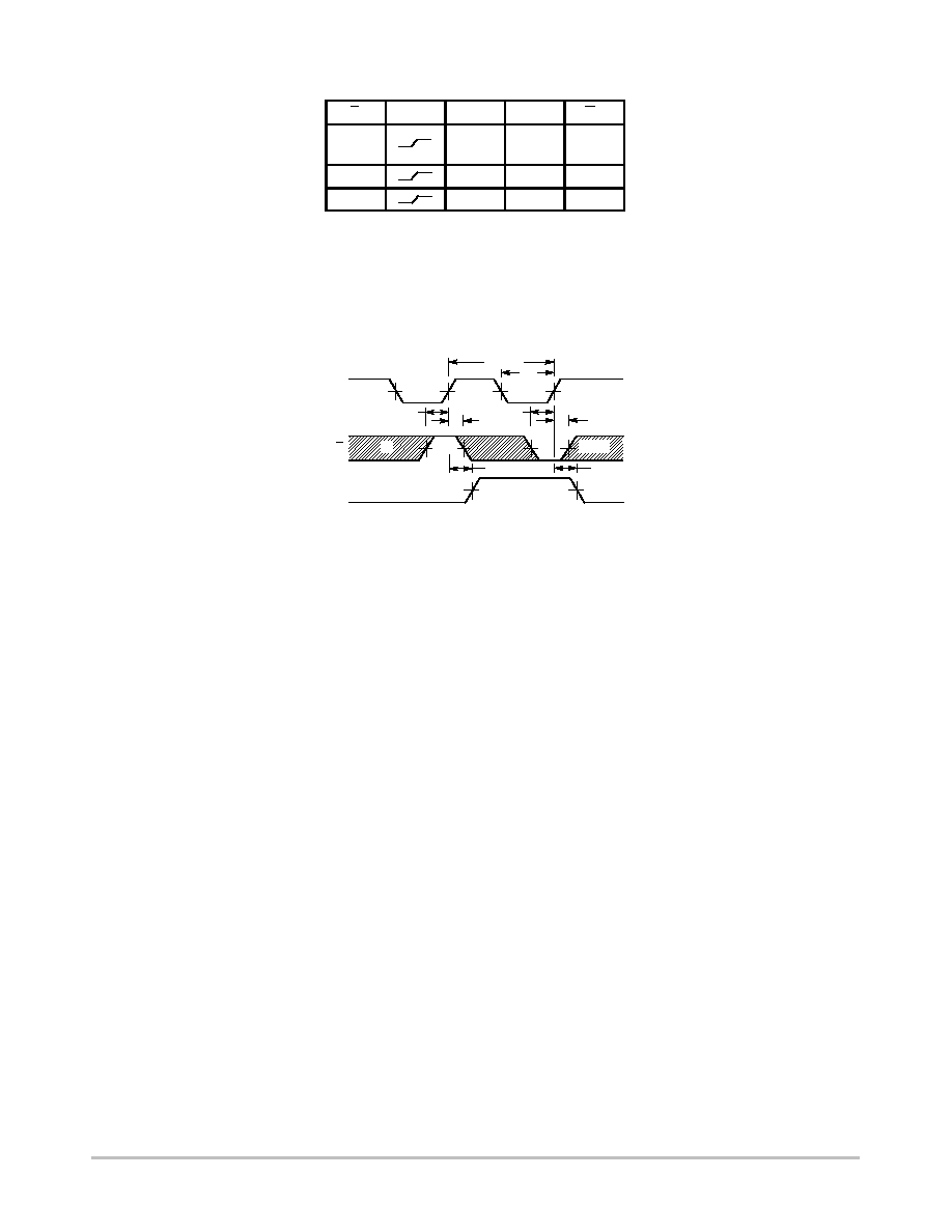
AC WAVEFORM
*The shaded areas indicate when the input is permitted to
change for predictable output performance.
1.3 V
1.3 V
1.3 V
1.3 V
1.3 V
1.3 V
1/f
max
t
W
t
s(H)
t
h(H)
t
s(L)
t
h(L)
CP
t
PHL
t
PLH
D OR E
Q
*
SN74LS377
http://onsemi.com
5
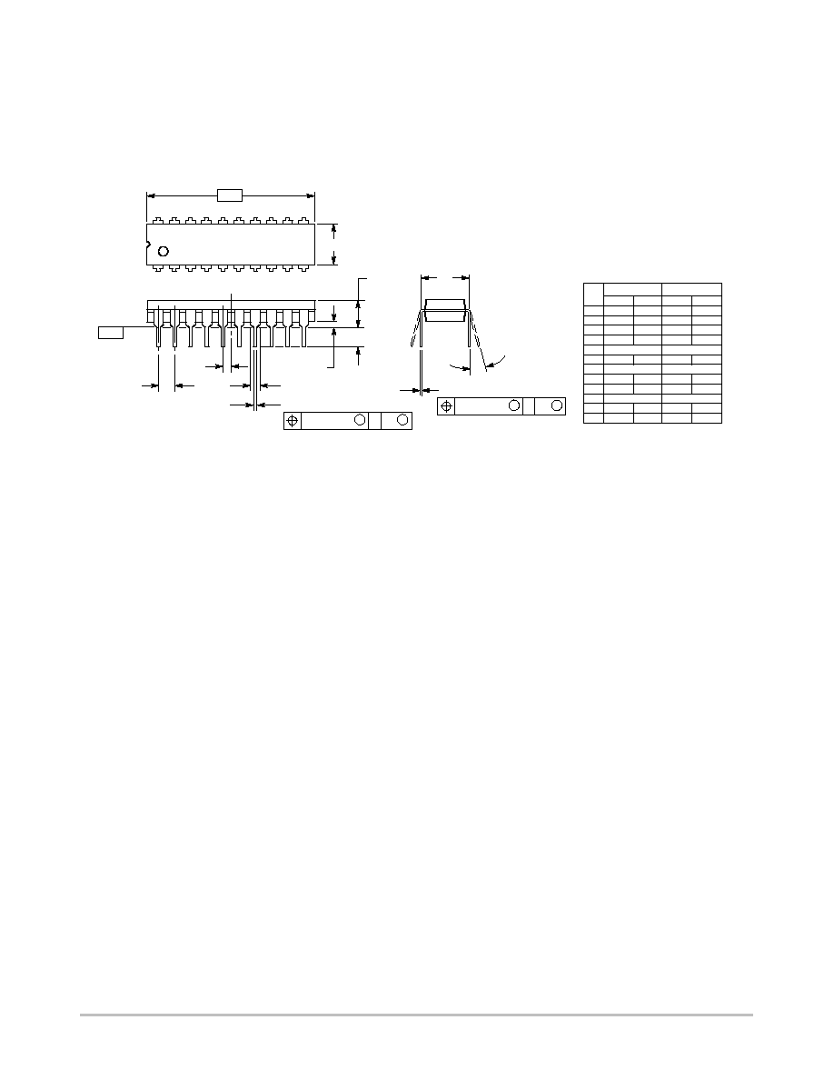
PACKAGE DIMENSIONS
N SUFFIX
PLASTIC PACKAGE
CASE 738≠03
ISSUE E
NOTES:
1. DIMENSIONING AND TOLERANCING PER ANSI
Y14.5M, 1982.
2. CONTROLLING DIMENSION: INCH.
3. DIMENSION L TO CENTER OF LEAD WHEN
FORMED PARALLEL.
4. DIMENSION B DOES NOT INCLUDE MOLD
FLASH.
M
L
J
20 PL
M
B
M
0.25 (0.010)
T
DIM
MIN
MAX
MIN
MAX
MILLIMETERS
INCHES
A
25.66
27.17
1.010
1.070
B
6.10
6.60
0.240
0.260
C
3.81
4.57
0.150
0.180
D
0.39
0.55
0.015
0.022
G
2.54 BSC
0.100 BSC
J
0.21
0.38
0.008
0.015
K
2.80
3.55
0.110
0.140
L
7.62 BSC
0.300 BSC
M
0
15
0
15
N
0.51
1.01
0.020
0.040
_
_
_
_
E
1.27
1.77
0.050
0.070
1
11
10
20
≠A≠
SEATING
PLANE
K
N
F
G
D
20 PL
≠T≠
M
A
M
0.25 (0.010)
T
E
B
C
F
1.27 BSC
0.050 BSC