 | –≠–ª–µ–∫—Ç—Ä–æ–Ω–Ω—ã–π –∫–æ–º–ø–æ–Ω–µ–Ω—Ç: SS16T3G | –°–∫–∞—á–∞—Ç—å:  PDF PDF  ZIP ZIP |
©
Semiconductor Components Industries, LLC, 2005
July, 2005 - Rev. 6
1
Publication Order Number:
SS16/D
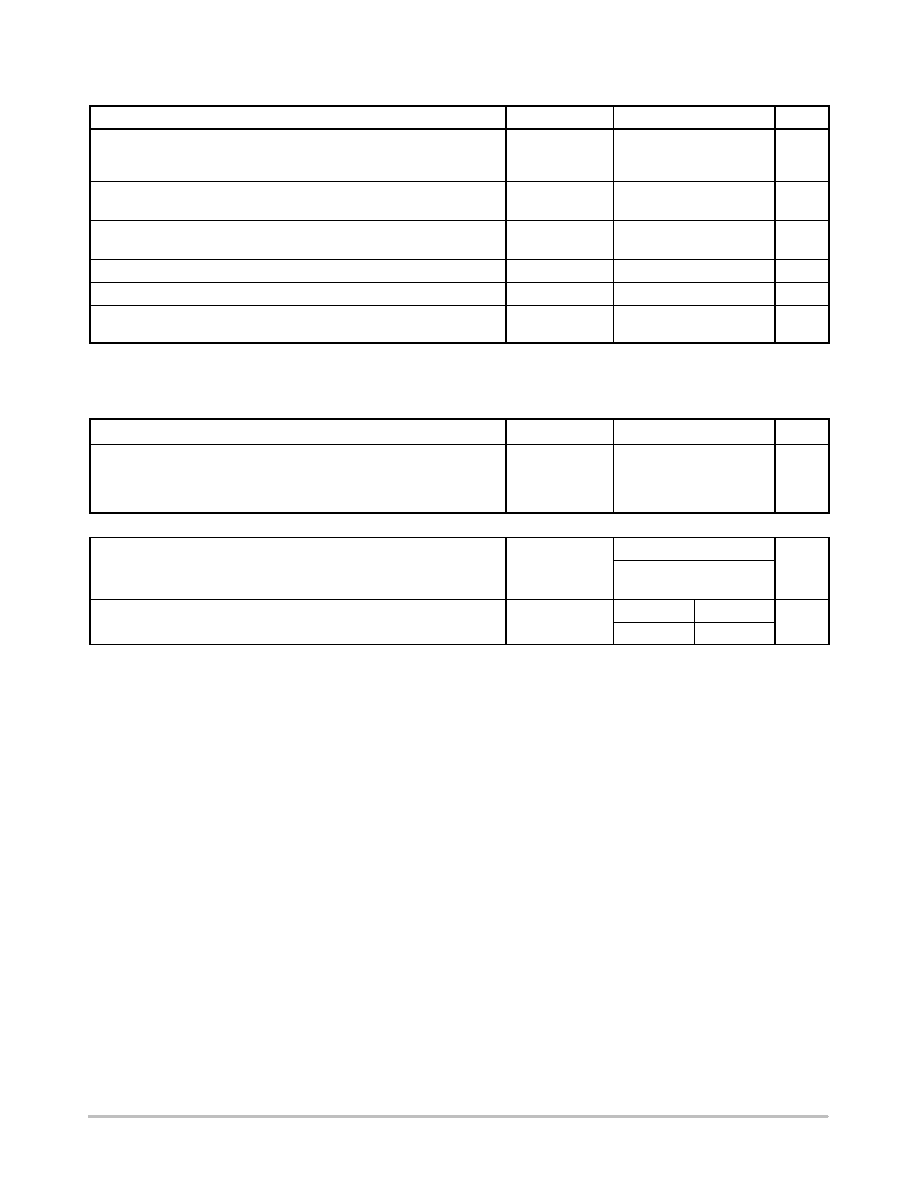
SS16
Surface Mount
Schottky Power Rectifier
SMA Power Surface Mount Package
These devices employ the Schottky Barrier principle in a large area
metal-to-silicon power diode. State of the art geometry features
epitaxial construction with oxide passivation and metal overlay
contact. Ideally suited for low voltage, high frequency rectification, or
as free wheeling and polarity diodes in surface mount applications
where compact size and weight are critical to the system.
Features
∑
Small Compact Surface Mountable Package with J-Bent Leads
∑
Rectangular Package for Automated Handling
∑
Highly Stable Oxide Passivated Junction
∑
Very Low Forward Voltage Drop
∑
Guardring for Stress Protection
∑
Pb-Free Package is Available
Mechanical Characteristics
∑
Case: Epoxy, Molded, Epoxy Meets UL 94 V-0
∑
Weight: 70 mg (approximately)
∑
Finish: All External Surfaces Corrosion Resistant and Terminal
Leads are Readily Solderable
∑
Lead and Mounting Surface Temperature for Soldering Purposes:
260
∞C Max. for 10 Seconds
∑
Shipped in 12 mm tape, 5000 units per 13 inch reel
∑
Polarity: Cathode Lead Indicated by Polarity Band
∑
ESD Ratings:
Machine Model = C
Human Body Model = 3B
∑
Device Meets MSL 1 Requirements
Device
Package
Shipping
ORDERING INFORMATION
SS16T3
SMA
5000/Tape & Reel
SCHOTTKY BARRIER
RECTIFIER
1.0 AMPERES
60 VOLTS
SMA
CASE 403D
PLASTIC
http://onsemi.com
For information on tape and reel specifications,
including part orientation and tape sizes, please
refer to our Tape and Reel Packaging Specification
Brochure, BRD8011/D.
SS16T3G
SMA
(Pb-Free)
5000/Tape & Reel
MARKING DIAGRAM
SS16
= Specific Device Code
A
= Assembly Location
Y
= Year
WW
= Work Week
G
= Pb-Free Package
SS16
AYWW
G
SS16
http://onsemi.com
2
MAXIMUM RATINGS
Rating
Symbol
Value
Unit
Peak Repetitive Reverse Voltage
Working Peak Reverse Voltage
DC Blocking Voltage
V
RRM
V
RWM
V
R
60
V
Average Rectified Forward Current
(At Rated V
R
, T
C
= 105
∞
C)
I
O
1.0
A
Non-Repetitive Peak Surge Current
(Surge Applied at Rated Load Conditions Halfwave, Single Phase, 60 Hz)
I
FSM
40
A
Storage/Operating Case Temperature
T
stg
, T
C
-55 to +150
∞
C
Operating Junction Temperature
T
J
-55 to +150
∞
C
Voltage Rate of Change
(Rated V
R
, T
J
= 25
∞
C)
dv/dt
10,000
V/
m
s
Maximum ratings are those values beyond which device damage can occur. Maximum ratings applied to the device are individual stress limit
values (not normal operating conditions) and are not valid simultaneously. If these limits are exceeded, device functional operation is not implied,
damage may occur and reliability may be affected.
THERMAL CHARACTERISTICS
Characteristic
Symbol
Value
Unit
Thermal Resistance,
Junction-to-Lead (Note 1)
Thermal Resistance,
Junction-to-Ambient (Note 1)
R
q
JL
R
q
JA
35
86
∞
C/W
ELECTRICAL CHARACTERISTICS
Maximum Instantaneous Forward Voltage
(Note 2)
(I
F
= 0.1 A)
(I
F
= 1.0 A)
V
F
T
J
= 25
∞
C
V
0.51
0.72
Maximum Instantaneous Reverse Current
(V
R
= 60 V)
I
R
T
J
= 25
∞
C
T
J
= 100
∞
C
mA
0.2
5.0
1. Mounted on 2 in Square PC Board with 1 in Square Total Pad Size, PC Board FR4.
2. Pulse Test: Pulse Width
250
m
s, Duty Cycle
2.0%.
SS16
http://onsemi.com
3
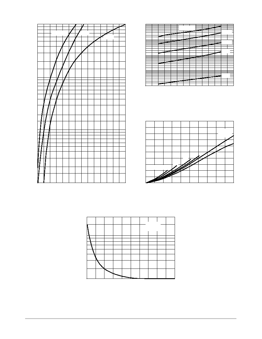
Figure 1. Typical Forward Voltage
Figure 2. Typical Reverse Current*
Figure 3. Forward Power Dissipation
1.4
v
F
, INSTANTANEOUS VOLTAGE (VOLTS)
10
1.0
V
R
, REVERSE VOLTAGE (VOLTS)
40
70
0
0.1
0.05
0.001
I
F(AV)
, AVERAGE FORWARD CURRENT (AMPS)
1.0
0
4.0
2.0
0
2.0
i F
, INST
ANT
ANEOUS
FOR
W
ARD
CURRENT
(AMPS)
I
P
F(A
V)
, A
VERAGE
FOR
W
ARD
0.1
0.6
0.2
0.4
0.8
1.0
50
60
10
20
30
10
3.0
4.0
5.0
0
1.6
5.0
3.0
1.0
, REVERSE CURRENT
(mA)
R
0.2
0.5
1.0
0.02
0.01
0.005
0.002
T
J
= 150∞C
100∞C
25∞C
I
PK
/I
AV
= 20
SQUARE
WAVE
dc
10
5
T
J
= 150∞C
*The curves shown are typical for the highest voltage device in the volt-
age grouping. Typical reverse current for lower voltage selections can
be estimated from these same curves if V
R
is sufficiently below rated V
R
.
125∞C
5.0
2.0
100∞C
75∞C
25∞C
POWER DISSIP
A
TION
(W
A
TTS)
1.2
0.07
0.05
0.03
0.02
0.2
0.3
0.5
0.7
2.0
3.0
5.0
7.0
p
Figure 4. Typical Capacitance
V
R
, REVERSE VOLTAGE (VOLTS)
50
80
0
60
40
30
20
60
70
10
20
30
40
50
70
80
100
200
C, CAP
ACIT
ANCE
(pF)
100
90
T
J
= 25∞C
f = 1 MHz
SS16
http://onsemi.com
4
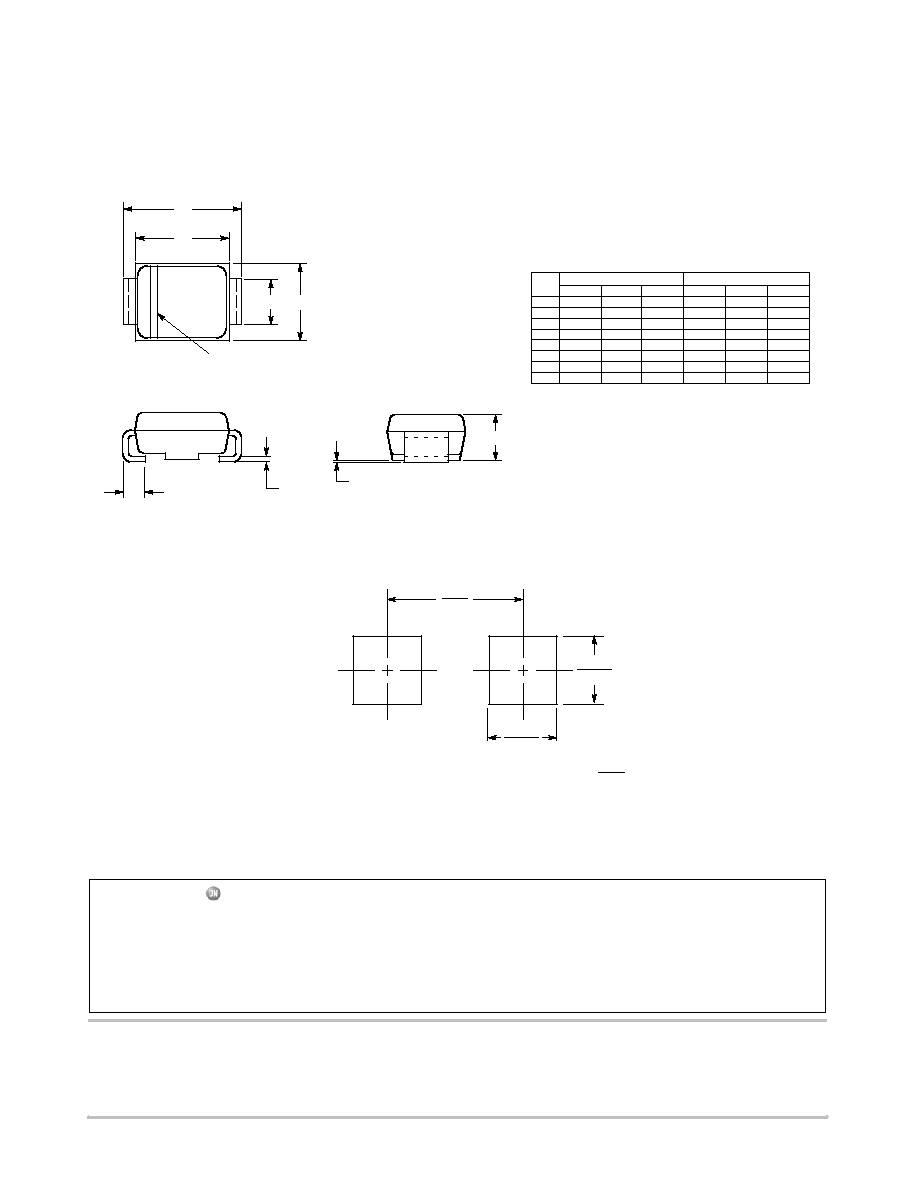
PACKAGE DIMENSIONS
SMA
CASE 403D-02
ISSUE C
4.0
0.157
2.0
0.0787
2.0
0.0787
mm
inches
SCALE 8:1
*For additional information on our Pb-Free strategy and soldering
details, please download the ON Semiconductor Soldering and
Mounting Techniques Reference Manual, SOLDERRM/D.
SOLDERING FOOTPRINT*
DIM
A
MIN
NOM
MAX
MIN
MILLIMETERS
1.91
2.16
2.41
0.075
INCHES
A1
0.05
0.10
0.15
0.002
b
1.27
1.45
1.63
0.050
c
0.15
0.28
0.41
0.006
D
2.29
2.60
2.92
0.090
E
4.06
4.32
4.57
0.160
L
0.76
1.14
1.52
0.030
0.085
0.095
0.004
0.006
0.057
0.064
0.011
0.016
0.103
0.115
0.170
0.180
0.045
0.060
NOM
MAX
4.83
5.21
5.59
0.190
0.205
0.220
H
E
E
b
D
L
c
A
A1
NOTES:
1. DIMENSIONING AND TOLERANCING PER ANSI
Y14.5M, 1982.
2. CONTROLLING DIMENSION: INCH.
3. 403D-01 OBSOLETE, NEW STANDARD IS 403D-02.
POLARITY INDICATOR
OPTIONAL AS NEEDED
(SEE STYLES)
H
E
STYLE 1:
PIN 1. CATHODE (POLARITY BAND)
2. ANODE
ON Semiconductor and are registered trademarks of Semiconductor Components Industries, LLC (SCILLC). SCILLC reserves the right to make changes without further notice
to any products herein. SCILLC makes no warranty, representation or guarantee regarding the suitability of its products for any particular purpose, nor does SCILLC assume any liability
arising out of the application or use of any product or circuit, and specifically disclaims any and all liability, including without limitation special, consequential or incidental damages.
"Typical" parameters which may be provided in SCILLC data sheets and/or specifications can and do vary in different applications and actual performance may vary over time. All
operating parameters, including "Typicals" must be validated for each customer application by customer's technical experts. SCILLC does not convey any license under its patent rights
nor the rights of others. SCILLC products are not designed, intended, or authorized for use as components in systems intended for surgical implant into the body, or other applications
intended to support or sustain life, or for any other application in which the failure of the SCILLC product could create a situation where personal injury or death may occur. Should
Buyer purchase or use SCILLC products for any such unintended or unauthorized application, Buyer shall indemnify and hold SCILLC and its officers, employees, subsidiaries, affiliates,
and distributors harmless against all claims, costs, damages, and expenses, and reasonable attorney fees arising out of, directly or indirectly, any claim of personal injury or death
associated with such unintended or unauthorized use, even if such claim alleges that SCILLC was negligent regarding the design or manufacture of the part. SCILLC is an Equal
Opportunity/Affirmative Action Employer. This literature is subject to all applicable copyright laws and is not for resale in any manner.
PUBLICATION ORDERING INFORMATION
N. American Technical Support: 800-282-9855 Toll Free
USA/Canada
Japan: ON Semiconductor, Japan Customer Focus Center
2-9-1 Kamimeguro, Meguro-ku, Tokyo, Japan 153-0051
Phone: 81-3-5773-3850
SS16/D
LITERATURE FULFILLMENT:
Literature Distribution Center for ON Semiconductor
P.O. Box 61312, Phoenix, Arizona 85082-1312 USA
Phone: 480-829-7710 or 800-344-3860 Toll Free USA/Canada
Fax: 480-829-7709 or 800-344-3867 Toll Free USA/Canada
Email: orderlit@onsemi.com
ON Semiconductor Website: http://onsemi.com
Order Literature: http://www.onsemi.com/litorder
For additional information, please contact your
local Sales Representative.