
©
Semiconductor Components Industries, LLC, 2002
July, 2002 ≠ Rev. 6
1
Publication Order Number:
STF202≠22T1/D
STF202-22
USB Filter with ESD
Protection
This device is designed for applications requiring Line
Termination, EMI Filtering and ESD Protection. It is intended for
use in upstream USB ports, Cellular phones, Wireless equipment and
computer applications. This device offers an integrated solution in a
small package (TSOP≠6, Case 318G) reducing PCB space and cost.
Features:
∑
Provides USB Line Termination, Filtering and ESD Protection
∑
Single IC Offers Cost Savings by Replacing 3 Resistors,
2 Capacitors, and 5 TVs diodes
∑
Bi≠directional EMI Filtering Prevents Noise from Entering/Leaving
the System
∑
IEC61000≠4≠2 ESD Protection for USB Port
∑
Flexible Pull≠down or Pull≠up Line Termination to Meet USB 1.1
Low Speed and High Speed Specification
∑
ESD Ratings: Machine Model = C
ESD Ratings:
Human Body Model = 3B
Benefits:
∑
TSOP≠6 Package Minimizes PCB Space
∑
Integrated Circuit Increases System Reliability versus Discrete
Component Implementation
∑
TVs Devices Provide ESD Protection That is Better than a Discrete
Implementation because the Small IC minimizes Parasitic
Inductances
Typical Applications:
∑
USB Hubs
∑
Computer Peripherals Using USB
MAXIMUM RATINGS
(T
A
= 25
∞
C)
Rating
Symbol
Value
Unit
Steady State Power
P
D
225
mW
Maximum Junction Temperature
T
J(max)
125
∞
C
Operating Temperature Range
T
J
≠55 to +125
∞
C
Storage Temperature Range
T
stg
≠55 to +125
∞
C
Lead Solder Temperature
(10 second duration)
T
L
260
∞
C
TSOP≠6
CASE 318G
STYLE 8
Device
Package
Shipping
ORDERING INFORMATION
STF202≠22T1
TSOP≠6
3000/Tape & Reel
CIRCUIT DESCRIPTION
S22 D
MARKING DIAGRAM
5
4
1
3
2
6
1
2
3
5
S22
= Specific Device Code
D
= Date Code
4
6
6
5
4
1
2
3
C
Rs1
R
up
C
Rs2
GND
D(OUT)
D(OUT)
V
BUS
D(IN)
D(IN)
http://onsemi.com

STF202≠22
http://onsemi.com
2
ELECTRICAL CHARACTERISTICS
(T
A
= 25
∞
C)
V
BR
@
1 mA
(Volts)
Max I
R
@ V
RWM
= 5.25 V
V
BUS
to
Max I
R
@ V
RWM
= 3.3 V
Typical Line
Capacitance
Series Resistor
R
S
(
W
) (Note 1)
Pull≠up Resistor
R
up
(k
W
)
Device
Device
Marking
V
RWM
(Volts)
Min
Max
V
BUS
to
GND
(
m
A)
= 3.3 V
I/O Pin
(
m
A)
Capacitance
(pF)
(Notes 2, 3)
Min
Nom
Max
Min
Nom
Max
STF202≠22T1
S22
5.25
6.0
8.0
5.0
1.0
68
20
22
24
1.35
1.5
1.65
1. For other R
S
values (i.e. R
S
= 30
W
) contact your local ON Semiconductor sales representative.
2. Measured at 25
∞
C, V
R
= 0 V, f = 1 MHz, Pins 2, 3, 4 or 5 to GND with Pin 1 also grounded.
3. For other capacitance values contact your local ON Semiconductor sales representative.
TYPICAL CHARACTERISTICS
Figure 1. Analog Cross≠talk (D+ to D≠)
Figure 2. Insertion Loss Characteristics
0.1
1
1000
10
100
P = ≠25 dBm
Vdc = 0 V
(MHz)
≠90
≠80
≠70
≠60
≠50
≠40
≠30
≠20
≠10
0
10
(dB)
0.1
1
1000
10
100
(MHz)
≠50
≠40
≠30
≠20
≠10
0
10
20
30
40
50
(dB)
P = ≠25 dBm
Vdc = 0 V
Figure 3. R
S
versus Temperature
Figure 4. R
up
versus Temperature
≠30
0
10
TARGET
TEMPERATURE (
∞
C)
21.0
21.2
21.4
21.6
21.8
22.0
22.2
R
S
(Ohms)
≠30
0
10
TEMPERATURE (
∞
C)
1450
1460
1470
1480
1490
1500
1510
1520
1530
1540
R
up
(Ohms)
R
S≠
TARGET
≠20 ≠10
20
30
40
50
60
70
80
≠20 ≠10
20
30
40
50
60
70
80

STF202≠22
http://onsemi.com
3
APPLICATIONS BACKGROUND
What Is USB?
The USB is not a serial port, it is a serial bus, a fact that
enables a single port on the computer to be a link for a myriad
of devices, (up to 127 devices in a USB system). We can
easily chain one device to another and use one port as a
connecting point of many devices by using a hub. All these
enables us to look at the USB system as a small network of
devices.
The Universal Serial Bus (USB) makes connecting
devices to your computer faster, easier and virtually
limitless. High≠Speed USB devices are capable of
communicating at speeds up to 12 megabits without shutting
down and without having to open your computer.
Figure 5. Typical USB System
SCANNER
PRINTER
HUB
MONITOR
KEYBOARD
COMPUTER PC
CPU
TELEPHONE
MOUSE
PLOTTER
Typically the USB system consists of one host, hubs and
devices.
The Host in the USB system, is responsible to the whole
complexity of the protocol (simplifies the designing of USB
devices). The host controls the media access, therefore, no
one can access the bus unless it got an approval required
from the host.
The Hub provides an interconnect point, which enables
many devices to connect to a single USB port. The logical
topology of the USB is a star structure, all the devices are
connected (logically) directly to the host. It is totally
transparent to the device what is its hub tier (the number of
hubs the data has to flow through). The hub is connected to
the USB host in the upstream direction (data flows "up" to
the host) and is connected to the USB device in the
downstream direction (data flows "down" from the host to
the device). The hub's main functionality is the
responsibility of detecting an attachment and detachment of
devices, handling the power management for devices that
are bus≠powered (get power from the bus), and
responsibility for bus error detection and recovery. Another
important role of the hub is to manage both full and low
speed devices. When a device is attached to the system the
hub detects the speed, which the device operates in, and
through the whole communication on the bus prevents from
full speed traffic to reach low speed device and vice versa ≠
prevent from low speed traffic to reach full speed device.
The Device is defined as everything in the USB system,
which is not a host (including hubs). A device provides one
or more USB functions. Most of the devices provide only
one function but there may be some, which provides more
than one and called compound devices. We refer to two
kinds of devices ≠ self powered or bus powered devices. A
device that gets its power from the bus is called bus powered
and on the other hand a device which supplies its own power
is called self powered. There are two kinds of devices:
Full≠speed devices ≠ operates in 12 Mb/s
Low≠speed devices that work in 1.5 Mb/s
STF202 Device Information
The Universal Serial Bus (USB) specification revision 1.1
requires EMI Filtering and line termination for the USB I/O
lines. The STF202 device from ON Semiconductor
provides upstream termination, EMI Filtering and ESD
Protection to IEC6100≠4≠2 (Level 4) in an integrated
solution placed in a small and single package (TSOP≠6,
Case 318G). The equivalent circuit of this device is shown
in the Figure 6.
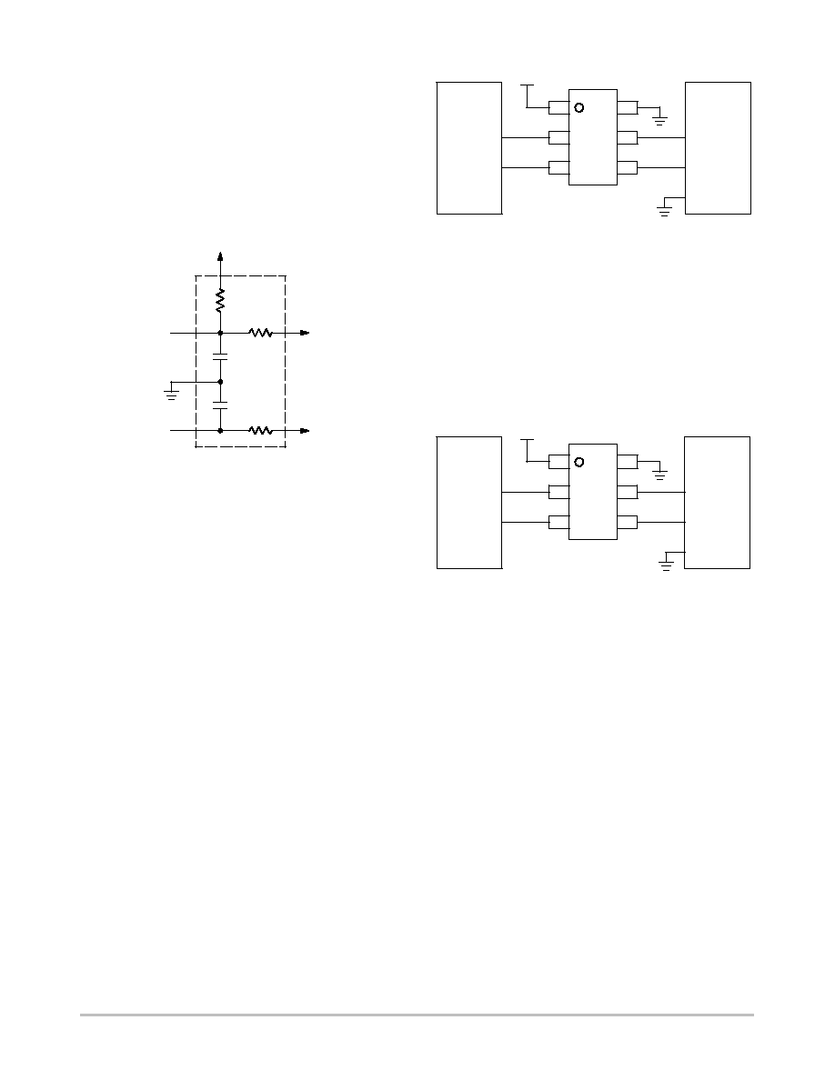
Rpu
C
C
GROUND
D
D
R
S1
R
S2
Figure 6.
STF202≠22
http://onsemi.com
4
As previously mentioned, there are two types of
configurations for the USB port which are upstream and
downstream. If your port connects to the host either in a
direct way or through a hub, you are upstream (data flows
"up" to the host) and in the other hand, if you are the host or
your port provides access to the host then you are
downstream (data flows "down" from the host to the
device). In the case of the STF202 device, it provides
upstream termination. The Figure 7 represents the
termination for an upstream USB port.
Figure 7.
Rpu
C
C
R
S
R
S
V
CC
The USB Line termination is reached through the series
resistors placed in the D+ and D≠ lines. These resistors
insure the proper termination to maintain the integrity of the
signal. The Pull up Resistor of 1.5 k
W on either the D+ or D≠
data lines is used to identify the equipment as either
full≠speed or low≠speed device.
Connection for Full≠Speed
and Low≠Speed Devices
As mentioned before, there are two kinds of port devices:
Full≠Speed devices ≠ operates in 12 Mb/s
Low≠Speed devices that work in 1.5 Mb/s
The STF202 device can be shaped to be used for either
Full≠Speed or Low≠Speed devices which is achieved as
described below:
Full≠Speed Devices
The Pull up resistor (Rpu) is connected to the D+ Line.
The terminal 1 is connected to the Voltage Supply Line
(V
BUS
) while the terminal 6 is connected to ground. The
input of the D+ line is connected in the terminal 3 which
outputs from the terminal 4. Finally, the input of the D≠ line
is connected in the terminal 2 which outputs from the
terminal 5. The Figure 8 shows the connections of the
STF202 device for "Full≠Speed devices".
Figure 8.
GND
D≠
D+
STF202
6
5
4
1
2
3
USB
Controller
D≠
D+
3.3 V
Peripheral
Low≠Speed Devices
The Pull up resistor (Rpu) is connected to the D≠ Line. The
terminal 1 is connected to the Voltage Supply Line (V
BUS
)
while the terminal 6 is connected to ground. The input of the
D≠ line is connected in the terminal 3 which outputs from the
terminal 4. Finally, the input of the D+ line is connected in
the terminal 2 which outputs from the terminal 5. The Figure
9 shows the connections of the STF202 device for
"Low≠Speed devices".
Figure 9.
GND
D+
D≠
STF202
6
5
4
1
2
3
USB
Controller
D+
D≠
3.3 V
Peripheral

STF202≠22
http://onsemi.com
5
The Figure 10 describes in a simplified way what the USB
port components are. As shown in this diagram, there are
signals for upstream and downstream ports which must be
provided with Line Termination and EMI Filtering to meet
the requirements of the USB specification revision 1.1. In
addition to the Line termination and EMI Filtering, it is also
needed to protect the USB I/O Lines against ESD
conditions, so TVS devices must be added for these
purposes.
Figure 10.
XTAL1
XTAL2
DPO
DMO
V
CC
GND
DP1≠DP4
DM1≠DM4
OC1≠OC4
PWR1≠PWR4
REGULATOR
POWER
SWITCHING
GND
V
BUS
D≠
D+
USB Data Lines
and Power to
Downstream
Ports
To
Upstream
Ports
CLK
CRISTAL
As mentioned before, the ON Semiconductor STF202
device provides "upstream termination", EMI Filtering and
ESD Protection to IEC6100≠4≠2 in an integrated solution
placed in a small and single package (TSOP≠6, Case 318G).
The typical application for the STF202 device is shown in
the Figure 11.
Figure 11.
D1D+
D1D≠
OC
PWR
DOD+
DOD≠
REGULATOR
TVS
V
BUS
D+
D≠
STF202
6
5
4
1
2
3
GND
OC
PWR
D2D+
D2D≠
TVS
POWER
SWITCH
V
BUS
D+
D≠
GND
DOWNSTREAM
TERMINATION
V
BUS
D+
D≠
GND
DOWNSTREAM
TERMINATION
USB CONTROLLER
STF202≠22
http://onsemi.com
6
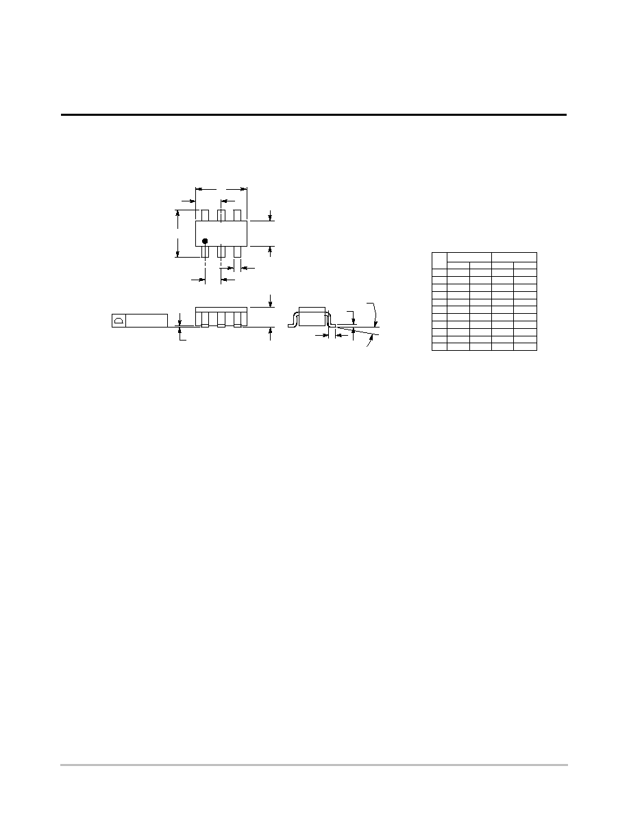
OUTLINE DIMENSIONS
EMI Filter with ESD Protection
TSOP≠6
CASE 318G≠02
ISSUE H
2
3
4
5
6
A
L
1
S
G
D
B
H
C
0.05 (0.002)
DIM
MIN
MAX
MIN
MAX
INCHES
MILLIMETERS
A
0.1142 0.1220
2.90
3.10
B
0.0512 0.0669
1.30
1.70
C
0.0354 0.0433
0.90
1.10
D
0.0098 0.0197
0.25
0.50
G
0.0335 0.0413
0.85
1.05
H
0.0005 0.0040
0.013
0.100
J
0.0040 0.0102
0.10
0.26
K
0.0079 0.0236
0.20
0.60
L
0.0493 0.0610
1.25
1.55
M
0
10
0
10
S
0.0985 0.1181
2.50
3.00
_
_
_
_
NOTES:
1. DIMENSIONING AND TOLERANCING PER ANSI
Y14.5M, 1982.
2. CONTROLLING DIMENSION: MILLIMETER.
3. MAXIMUM LEAD THICKNESS INCLUDES LEAD
FINISH THICKNESS. MINIMUM LEAD THICKNESS
IS THE MINIMUM THICKNESS OF BASE
MATERIAL.
M
J
K
STYLE 8:
PIN 1. Vbus
2. D(in)-
3. D(in)+
4. D(out)+
5. D(out)-
6. GND

STF202≠22
http://onsemi.com
7
Notes
STF202≠22
http://onsemi.com
8
ON Semiconductor and are registered trademarks of Semiconductor Components Industries, LLC (SCILLC). SCILLC reserves the right to make
changes without further notice to any products herein. SCILLC makes no warranty, representation or guarantee regarding the suitability of its products for any
particular purpose, nor does SCILLC assume any liability arising out of the application or use of any product or circuit, and specifically disclaims any and all
liability, including without limitation special, consequential or incidental damages. "Typical" parameters which may be provided in SCILLC data sheets and/or
specifications can and do vary in different applications and actual performance may vary over time. All operating parameters, including "Typicals" must be
validated for each customer application by customer's technical experts. SCILLC does not convey any license under its patent rights nor the rights of others.
SCILLC products are not designed, intended, or authorized for use as components in systems intended for surgical implant into the body, or other applications
intended to support or sustain life, or for any other application in which the failure of the SCILLC product could create a situation where personal injury or death
may occur. Should Buyer purchase or use SCILLC products for any such unintended or unauthorized application, Buyer shall indemnify and hold SCILLC
and its officers, employees, subsidiaries, affiliates, and distributors harmless against all claims, costs, damages, and expenses, and reasonable attorney fees
arising out of, directly or indirectly, any claim of personal injury or death associated with such unintended or unauthorized use, even if such claim alleges that
SCILLC was negligent regarding the design or manufacture of the part. SCILLC is an Equal Opportunity/Affirmative Action Employer.
PUBLICATION ORDERING INFORMATION
JAPAN: ON Semiconductor, Japan Customer Focus Center
4≠32≠1 Nishi≠Gotanda, Shinagawa≠ku, Tokyo, Japan 141≠0031
Phone: 81≠3≠5740≠2700
Email: r14525@onsemi.com
ON Semiconductor Website: http://onsemi.com
For additional information, please contact your local
Sales Representative.
STF202≠22T1/D
Literature Fulfillment:
Literature Distribution Center for ON Semiconductor
P.O. Box 5163, Denver, Colorado 80217 USA
Phone: 303≠675≠2175 or 800≠344≠3860 Toll Free USA/Canada
Fax: 303≠675≠2176 or 800≠344≠3867 Toll Free USA/Canada
Email: ONlit@hibbertco.com
N. American Technical Support: 800≠282≠9855 Toll Free USA/Canada