
©
Semiconductor Components Industries, LLC, 2002
May, 2002 ≠ Rev. 5
1
Publication Order Number:
TCA0372/D
TCA0372, TCA0372B
1.0 A Output Current,
Dual Power Operational
Amplifiers
The TCA0372 is a monolithic circuit intended for use as a power
operational amplifier in a wide range of applications, including servo
amplifiers and power supplies. No deadband crossover distortion
provides better performance for driving coils.
∑
Output Current to 1.0 A
∑
Slew Rate of 1.3 V/
ms
∑
Wide Bandwidth of 1.1 MHz
∑
Internal Thermal Shutdown
∑
Single or Split Supply Operation
∑
Excellent Gain and Phase Margins
∑
Common Mode Input Includes Ground
∑
Zero Deadband Crossover Distortion
Figure 1. Representative Block Diagram
V
EE
V
CC
Output
Thermal
Protection
Current
Bias
Monitoring
Inv.
Input
Noninv.
Input
Device
Package
Shipping
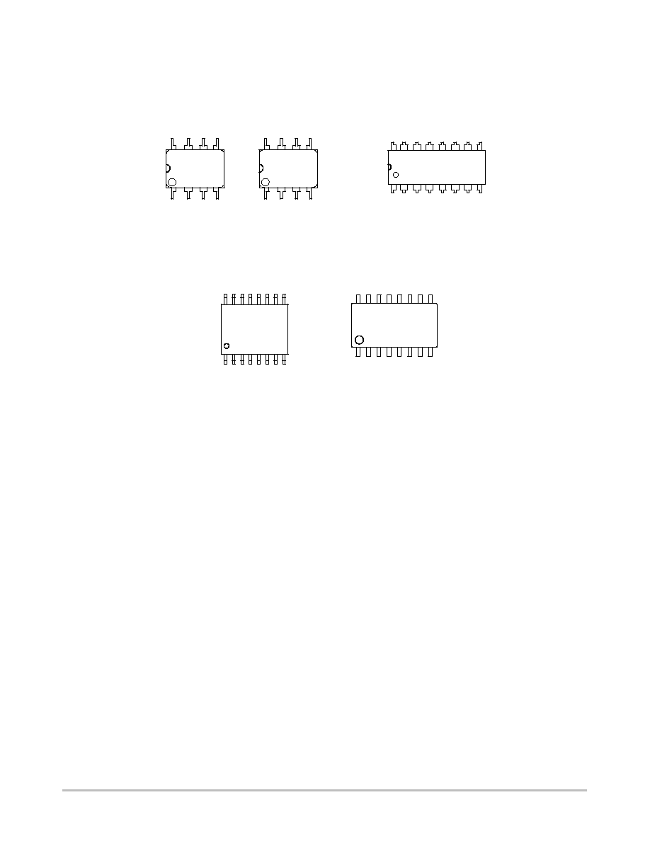
ORDERING INFORMATION
TCA0372DW
SO≠16W
47 Units/Rail
TCA0372DP1
PDIP≠8
TCA0372BDP1
PDIP≠8
PDIP≠8
DP1 SUFFIX
CASE 626
1
8
50 Units/Rail
50 Units/Rail
TCA0372DP2
PDIP≠16
25 Units/Rail
TCA0372DWR2
SO≠16W
1000 Tape & Reel
TCA0372DM2EL SOEIAJ≠16
2500 Tape & Reel
1
16
PDIP≠16
DP2 SUFFIX
CASE 648
1
16
SO≠16W
DW SUFFIX
CASE 751G
1
16
SOEIAJ≠16
DM2 SUFFIX
CASE 966
See general marking information in the device marking
section on page 6 of this data sheet.
DEVICE MARKING INFORMATION
http://onsemi.com

TCA0372, TCA0372B
http://onsemi.com
2
PIN CONNECTIONS
(Top View)
CASE 648
Output A
V
CC
Output B
V
EE
/Gnd
Inputs B
Inputs A
Gnd
Gnd
Gnd
Gnd
Gnd
Gnd
Gnd
Gnd
16
15
14
13
12
11
10
9
1
2
3
4
5
6
7
8
+
+
-
-
*Pins 4 and 9 to 16 are internally connected.
CASE 751G
V
CC
Output B
NC
V
EE
/Gnd
NC
Output A
NC
NC
V
EE
/Gnd
NC
16
15
14
13
12
11
10
9
1
2
3
4
5
6
7
8
(Top View)
(Top View)
Output A
V
EE
/Gnd
+
-
CASE 626
1
2
3
4
8
7
6
5
+
-
V
CC
Output B
Inputs A
Inputs B
Inputs B
Inputs A
+
-
+ -
CASE 966
V
EE
/Gnd
NC
Output A
NC
V
EE
/Gnd
NC
Inputs A
16
15
14
13
12
11
10
9
1
2
3
4
5
6
7
8
(Top View)
V
CC
Output B
NC
V
EE
/Gnd
Inputs B
NC
V
EE
/Gnd
+
-
+
-
MAXIMUM RATINGS
Rating
Symbol
Value
Unit
Supply Voltage (from V
CC
to V
EE
)
V
S
40
V
Input Differential Voltage Range
V
IDR
Note 1
V
Input Voltage Range
V
IR
Note 1
V
Junction Temperature (Note 2)
T
J
+150
∞
C
Operating Temperature Range
T
A
≠40 to +125
∞
C
Storage Temperature Range
T
stg
≠55 to +150
∞
C
DC Output Current
I
O
1.0
A
Peak Output Current (Nonrepetitive)
I
(max)
1.5
A
Thermal Resistance, Junction≠to≠Air
Case 626
Case 648
Case 751G
R
q
JA
137
72
80
∞
C/W
Thermal Resistance, Junction≠to≠Case
Case 626
Case 648
Case 751G
R
q
JC
23
10
12
∞
C/W
1. Either or both input voltages should not exceed the magnitude of V
CC
or V
EE
.
2. Power dissipation must be considered to ensure maximum junction temperature (T
J
) is not exceeded.

TCA0372, TCA0372B
http://onsemi.com
3
DC ELECTRICAL CHARACTERISTICS
(V
CC
= +15 V, V
EE
= ≠15 V, R
L
connected to ground, T
A
= ≠40
∞
to +125
∞
C.)
Characteristics
Symbol
Min
Typ
Max
Unit
Input Offset Voltage (V
CM
= 0)
T
A
= +25
∞
C
T
A
, T
low
to T
high
V
IO
≠
≠
1.0
≠
15
20
mV
Average Temperature Coefficient of Offset Voltage
D
V
IO
/
D
T
≠
20
≠
m
V/
∞
C
Input Bias Current (V
CM
= 0)
I
IB
≠
100
500
nA
Input Offset Current (V
CM
= 0)
I
IO
≠
10
50
nA
Large Signal Voltage Gain
V
O
=
±
10 V, R
L
= 2.0 k
A
VOL
30
100
≠
V/mV
Output Voltage Swing (I
L
= 100 mA)
T
A
= +25
∞
C
T
A
= T
low
to T
high
T
A
= +25
∞
C
T
A
= T
low
to T
high
V
OH
V
OL
14.0
13.9
≠
≠
14.2
≠
≠14.2
≠
≠
≠
≠14.0
≠13.9
V
Output Voltage Swing (I
L
= 1.0 A)
V
CC
= +24 V, V
EE
= 0 V, T
A
= +25
∞
C
V
CC
= +24 V, V
EE
= 0 V, T
A
= T
low
to T
high
V
CC
= +24 V, V
EE
= 0 V, T
A
= +25
∞
C
V
CC
= +24 V, V
EE
= 0 V, T
A
= T
low
to T
high
V
OH
V
OL
22.5
22.5
≠
≠
22.7
≠
1.3
≠
≠
≠
1.5
1.5
V
Input Common Mode Voltage Range
T
A
= +25
∞
C
T
A
= T
low
to T
high
V
ICR
V
EE
to (V
CC
≠1.0)
V
EE
to (V
CC
≠1.3)
V
Common Mode Rejection Ratio (R
S
= 10 k)
CMRR
70
90
≠
dB
Power Supply Rejection Ratio (R
S
= 100
W
)
PSRR
70
90
≠
dB
Power Supply Current
T
A
= +25
∞
C
TCA0372
TCA0372B
T
A
= T
low
to T
high
TCA0372
TCA0372B
I
D
≠
≠
≠
≠
5.0
8.0
≠
≠
10
10
14
14
mA
AC ELECTRICAL CHARACTERISTICS
(V
CC
= +15 V, V
EE
= ≠15 V, R
L
connected to ground, T
A
= +25
∞
C, unless otherwise noted.)
Characteristics
Symbol
Min
Typ
Max
Unit
Slew Rate (V
in
= ≠10 V to +10 V, R
L
= 2.0 k, C
L
= 100 pF)
A
V
= ≠1.0, T
A
= T
low
to T
high
SR
1.0
1.4
≠
V/
m
s
Gain Bandwidth Product (f = 100 kHz, C
L
= 100 pF, R
L
= 2.0 k)
T
A
= 25
∞
C
T
A
= T
low
to T
high
GBW
0.9
0.7
1.4
≠
≠
≠
MHz
Phase Margin T
J
= T
low
to T
high
R
L
= 2.0 k, C
L
= 100 pF
f
m
≠
65
≠
Degrees
Gain Margin
R
L
= 2.0 k, C
L
= 100 pF
A
m
≠
15
≠
dB
Equivalent Input Noise Voltage
R
S
= 100
W
, f = 1.0 to 100 kHz
e
n
≠
22
≠
nV/ Hz
Total Harmonic Distortion
A
V
= ≠1.0, R
L
= 50
W
, V
O
= 0.5 VRMS, f = 1.0 kHz
THD
≠
0.02
≠
%
NOTE: In case V
EE
is disconnected before V
CC
, a diode between V
EE
and Ground is recommended to avoid damaging the device.
TCA0372, TCA0372B
http://onsemi.com
4
V
CC
= +15 V
V
EE
= -15 V
R
L
= 2.0 kW
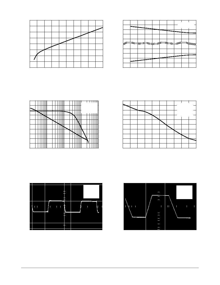
Figure 2. Supply Current versus Supply
Voltage with No Load
Figure 3. Output Saturation Voltage
versus Load Current
Figure 4. Voltage Gain and Phase
versus Frequency
Figure 5. Phase Margin versus Output
Load Capacitance
Figure 6. Small Signal Transient Response
Figure 7. Large Signal Transient Response
V O
,
OUTPUT
VOL
T
AGE (50 mV/DIV)
t, TIME (1.0 ms/DIV)
V O
,
OUTPUT
VOL
T
AGE (5.0 V/DIV)
t, TIME (10 ms/DIV)
, SUPPL
Y
CURRENT
(mA)
I CC
6.5
5.5
4.5
3.5
2.5
0
2.0
4.0
6.0
8.0
10
12
14
16
18
20
V
CC
, |V
EE
|, SUPPLY VOLTAGE (V)
0
1.0
0.5
I
L
, LOAD CURRENT (A)
, OUTPUT
SA
TURA
TION VOL
T
AGE (V)
V sat
80
40
20
-20
1.0
10
100
1000
10000
130
120
110
100
90
80
f, FREQUENCY (kHz)
PHASE (DEGREES)
GAIN (dB)
0.4
C
L
, OUTPUT LOAD CAPACITANCE (nF)
, PHASE MARGIN (DEGREES)
m
60
70
50
40
30
20
0
0.8
1.2
1.6
2.0
V
CC
= +15 V
V
EE
= -15 V
R
L
= 2.0 kW
A
V
= -100
V
CC
= 24 V
V
EE
= 0 V
60
V
CC
= +15 V
V
EE
= -15 V
A
V
= +1.0
R
L
= 2.0 kW
V
CC
= +15 V
V
EE
= -15 V
A
V
= +1.0
R
L
= 2.0 kW
V
CC
V
CC
-1.0
V
CC
-2.0
V
CC
+2.0
V
EE
V
CC
+1.0

TCA0372, TCA0372B
http://onsemi.com
5
V
CC
= +15 V
V
EE
= -15 V
A
V
= +100
R
L
= 50 W
t, TIME (100 ms/DIV)
Figure 8. Sine Wave Response
5.0 V/DIV
200 mV/DIV
Figure 9. Bidirectional DC Motor Control with
Microprocessor≠Compatible Inputs
V
S
= Logic Supply Voltage
Must Have V
CC
> V
S
E1, E2 = Logic Inputs
+
-
+
-
V
CC
E2
E1
V
S
/2
R7
R1
V
in
R2
5.0 W
R5
R6
10 k
R
x
R3
0.1 mF
R8
10 k
+
-
+
-
V
S
0.1 mF
10 k
10 k
10 k
10 k
Figure 10. Bidirectional Speed Control of DC Motors
For circuit stability, ensure that R
x
>
where, R
M
= internal resistance of motor.
The voltage available at the terminals of the motor is:
where, |R
o
| =
and I
M
is the motor current.
2R3 @ R1
RM
VM + 2 (V1
VS
2 ) ) |Ro| @ IM
2R3 @ R1
Rx
TCA0372, TCA0372B
http://onsemi.com
6
PDIP≠8
DP1 SUFFIX
CASE 626
MARKING DIAGRAMS
A
= Assembly Location
WL, L
= Wafer Lot
YY, Y
= Year
WW, W
= Work Week
1
8
0372DP1
AWL
YYWW
0372BDP1
AWL
YYWW
PDIP≠16
DP2 SUFFIX
CASE 648
1
8
1
16
TCA0372DP2
AWLYYWW
SO≠16W
DW SUFFIX
CASE 751G
TCA0372DW
AWLYYWW
1
16
SOEIAJ≠16
DM2 SUFFIX
CASE 966
TCA0372
ALYW
16
1
TCA0372, TCA0372B
http://onsemi.com
7
PACKAGE DIMENSIONS
PDIP≠8
DP1 SUFFIX
CASE 626≠05
ISSUE L
NOTES:
1. DIMENSION L TO CENTER OF LEAD WHEN
FORMED PARALLEL.
2. PACKAGE CONTOUR OPTIONAL (ROUND OR
SQUARE CORNERS).
3. DIMENSIONING AND TOLERANCING PER ANSI
Y14.5M, 1982.
1
4
5
8
F
NOTE 2
≠A≠
≠B≠
≠T≠
SEATING
PLANE
H
J
G
D
K
N
C
L
M
M
A
M
0.13 (0.005)
B
M
T
DIM
MIN
MAX
MIN
MAX
INCHES
MILLIMETERS
A
9.40
10.16
0.370
0.400
B
6.10
6.60
0.240
0.260
C
3.94
4.45
0.155
0.175
D
0.38
0.51
0.015
0.020
F
1.02
1.78
0.040
0.070
G
2.54 BSC
0.100 BSC
H
0.76
1.27
0.030
0.050
J
0.20
0.30
0.008
0.012
K
2.92
3.43
0.115
0.135
L
7.62 BSC
0.300 BSC
M
---
10
---
10
N
0.76
1.01
0.030
0.040
_
_
PDIP≠16
DP2 SUFFIX
CASE 648≠08
ISSUE R
NOTES:
1. DIMENSIONING AND TOLERANCING PER ANSI
Y14.5M, 1982.
2. CONTROLLING DIMENSION: INCH.
3. DIMENSION L TO CENTER OF LEADS WHEN
FORMED PARALLEL.
4. DIMENSION B DOES NOT INCLUDE MOLD FLASH.
5. ROUNDED CORNERS OPTIONAL.
≠A≠
B
F
C
S
H
G
D
J
L
M
16 PL
SEATING
1
8
9
16
K
PLANE
≠T≠
M
A
M
0.25 (0.010)
T
DIM
MIN
MAX
MIN
MAX
MILLIMETERS
INCHES
A
0.740
0.770
18.80
19.55
B
0.250
0.270
6.35
6.85
C
0.145
0.175
3.69
4.44
D
0.015
0.021
0.39
0.53
F
0.040
0.70
1.02
1.77
G
0.100 BSC
2.54 BSC
H
0.050 BSC
1.27 BSC
J
0.008
0.015
0.21
0.38
K
0.110
0.130
2.80
3.30
L
0.295
0.305
7.50
7.74
M
0
10
0
10
S
0.020
0.040
0.51
1.01
_
_
_
_
TCA0372, TCA0372B
http://onsemi.com
8
PACKAGE DIMENSIONS
SO≠16W
DW SUFFIX
CASE 751G≠03
ISSUE B
D
14X
B
16X
SEATING
PLANE
S
A
M
0.25
B
S
T
16
9
8
1
h
X 45
_
M
B
M
0.25
H
8X
E
B
A
e
T
A1
A
L
C
q
NOTES:
1. DIMENSIONS ARE IN MILLIMETERS.
2. INTERPRET DIMENSIONS AND TOLERANCES
PER ASME Y14.5M, 1994.
3. DIMENSIONS D AND E DO NOT INLCUDE MOLD
PROTRUSION.
4. MAXIMUM MOLD PROTRUSION 0.15 PER SIDE.
5. DIMENSION B DOES NOT INCLUDE DAMBAR
PROTRUSION. ALLOWABLE DAMBAR
PROTRUSION SHALL BE 0.13 TOTAL IN EXCESS
OF THE B DIMENSION AT MAXIMUM MATERIAL
CONDITION.
DIM
MIN
MAX
MILLIMETERS
A
2.35
2.65
A1
0.10
0.25
B
0.35
0.49
C
0.23
0.32
D
10.15
10.45
E
7.40
7.60
e
1.27 BSC
H
10.05
10.55
h
0.25
0.75
L
0.50
0.90
q
0
7
_
_
SOEIAJ≠16
DM2 SUFFIX
CASE 966≠01
ISSUE O
H
E
A
1
DIM
MIN
MAX
MIN
MAX
INCHES
---
2.05
---
0.081
MILLIMETERS
0.05
0.20
0.002
0.008
0.35
0.50
0.014
0.020
0.18
0.27
0.007
0.011
9.90
10.50
0.390
0.413
5.10
5.45
0.201
0.215
1.27 BSC
0.050 BSC
7.40
8.20
0.291
0.323
0.50
0.85
0.020
0.033
1.10
1.50
0.043
0.059
0
0.70
0.90
0.028
0.035
---
0.78
---
0.031
A
1
H
E
Q
1
L
E
_
10
_
0
_
10
_
L
E
Q
1
_
NOTES:
1. DIMENSIONING AND TOLERANCING PER ANSI
Y14.5M, 1982.
2. CONTROLLING DIMENSION: MILLIMETER.
3. DIMENSIONS D AND E DO NOT INCLUDE MOLD
FLASH OR PROTRUSIONS AND ARE MEASURED
AT THE PARTING LINE. MOLD FLASH OR
PROTRUSIONS SHALL NOT EXCEED 0.15 (0.006)
PER SIDE.
4. TERMINAL NUMBERS ARE SHOWN FOR
REFERENCE ONLY.
5. THE LEAD WIDTH DIMENSION (b) DOES NOT
INCLUDE DAMBAR PROTRUSION. ALLOWABLE
DAMBAR PROTRUSION SHALL BE 0.08 (0.003)
TOTAL IN EXCESS OF THE LEAD WIDTH
DIMENSION AT MAXIMUM MATERIAL CONDITION.
DAMBAR CANNOT BE LOCATED ON THE LOWER
RADIUS OR THE FOOT. MINIMUM SPACE
BETWEEN PROTRUSIONS AND ADJACENT LEAD
TO BE 0.46 ( 0.018).
M
L
DETAIL P
VIEW P
c
A
b
e
M
0.13 (0.005)
0.10 (0.004)
1
16
9
8
D
Z
E
A
b
c
D
E
e
L
M
Z

TCA0372, TCA0372B
http://onsemi.com
9
Notes

TCA0372, TCA0372B
http://onsemi.com
10
Notes

TCA0372, TCA0372B
http://onsemi.com
11
Notes

TCA0372, TCA0372B
http://onsemi.com
12
ON Semiconductor and are registered trademarks of Semiconductor Components Industries, LLC (SCILLC). SCILLC reserves the right to make
changes without further notice to any products herein. SCILLC makes no warranty, representation or guarantee regarding the suitability of its products for any
particular purpose, nor does SCILLC assume any liability arising out of the application or use of any product or circuit, and specifically disclaims any and all
liability, including without limitation special, consequential or incidental damages. "Typical" parameters which may be provided in SCILLC data sheets and/or
specifications can and do vary in different applications and actual performance may vary over time. All operating parameters, including "Typicals" must be
validated for each customer application by customer's technical experts. SCILLC does not convey any license under its patent rights nor the rights of others.
SCILLC products are not designed, intended, or authorized for use as components in systems intended for surgical implant into the body, or other applications
intended to support or sustain life, or for any other application in which the failure of the SCILLC product could create a situation where personal injury or death
may occur. Should Buyer purchase or use SCILLC products for any such unintended or unauthorized application, Buyer shall indemnify and hold SCILLC
and its officers, employees, subsidiaries, affiliates, and distributors harmless against all claims, costs, damages, and expenses, and reasonable attorney fees
arising out of, directly or indirectly, any claim of personal injury or death associated with such unintended or unauthorized use, even if such claim alleges that
SCILLC was negligent regarding the design or manufacture of the part. SCILLC is an Equal Opportunity/Affirmative Action Employer.
PUBLICATION ORDERING INFORMATION
JAPAN: ON Semiconductor, Japan Customer Focus Center
4≠32≠1 Nishi≠Gotanda, Shinagawa≠ku, Tokyo, Japan 141≠0031
Phone: 81≠3≠5740≠2700
Email: r14525@onsemi.com
ON Semiconductor Website: http://onsemi.com
For additional information, please contact your local
Sales Representative.
TCA0372/D
Literature Fulfillment:
Literature Distribution Center for ON Semiconductor
P.O. Box 5163, Denver, Colorado 80217 USA
Phone: 303≠675≠2175 or 800≠344≠3860 Toll Free USA/Canada
Fax: 303≠675≠2176 or 800≠344≠3867 Toll Free USA/Canada
Email: ONlit@hibbertco.com
N. American Technical Support: 800≠282≠9855 Toll Free USA/Canada