 | –≠–ª–µ–∫—Ç—Ä–æ–Ω–Ω—ã–π –∫–æ–º–ø–æ–Ω–µ–Ω—Ç: TIP147 | –°–∫–∞—á–∞—Ç—å:  PDF PDF  ZIP ZIP |
1
Motorola Bipolar Power Transistor Device Data
Darlington Complementary
Silicon Power Transistors
. . . designed for general≠purpose amplifier and low frequency switching applications.
∑
High DC Current Gain -- Min hFE = 1000 @ IC = 5 A, VCE = 4 V
∑
Collector≠Emitter Sustaining Voltage -- @ 30 mA
VCEO(sus) = 60 Vdc (Min) -- TIP140, TIP145
VCEO(sus) =
80 Vdc (Min) -- TIP141, TIP146
VCEO(sus) =
100 Vdc (Min) -- TIP142, TIP147
∑
Monolithic Construction with Built≠In Base≠Emitter Shunt Resistor
ŒŒŒŒŒŒŒŒŒŒŒŒŒŒŒŒŒŒŒŒŒŒŒŒ
ŒŒŒŒŒŒŒŒŒŒŒŒŒŒŒŒŒŒŒŒŒŒŒŒ
MAXIMUM RATINGS
ŒŒŒŒŒŒŒŒŒŒŒ
Œ
ŒŒŒŒŒŒŒŒŒ
Œ
ŒŒŒŒŒŒŒŒŒŒŒ
Rating
ŒŒŒŒ
Œ
ŒŒ
Œ
ŒŒŒŒ
Symbol
ŒŒŒ
Œ
Œ
Œ
ŒŒŒ
TIP140
TIP145
ŒŒŒŒ
Œ
ŒŒ
Œ
ŒŒŒŒ
TIP141
TIP146
ŒŒŒŒ
Œ
ŒŒ
Œ
ŒŒŒŒ
TIP142
TIP147
ŒŒŒ
Œ
Œ
Œ
ŒŒŒ
Unit
ŒŒŒŒŒŒŒŒŒŒŒ
ŒŒŒŒŒŒŒŒŒŒŒ
Collector≠Emitter Voltage
ŒŒŒŒ
ŒŒŒŒ
VCEO
ŒŒŒ
ŒŒŒ
60
ŒŒŒŒ
ŒŒŒŒ
80
ŒŒŒŒ
ŒŒŒŒ
100
ŒŒŒ
ŒŒŒ
Vdc
ŒŒŒŒŒŒŒŒŒŒŒ
ŒŒŒŒŒŒŒŒŒŒŒ
Collector≠Base Voltage
ŒŒŒŒ
ŒŒŒŒ
VCB
ŒŒŒ
ŒŒŒ
60
ŒŒŒŒ
ŒŒŒŒ
80
ŒŒŒŒ
ŒŒŒŒ
100
ŒŒŒ
ŒŒŒ
Vdc
ŒŒŒŒŒŒŒŒŒŒŒ
ŒŒŒŒŒŒŒŒŒŒŒ
Emitter≠Base Voltage
ŒŒŒŒ
ŒŒŒŒ
VEB
ŒŒŒŒŒŒŒŒŒ
ŒŒŒŒŒŒŒŒŒ
5.0
ŒŒŒ
ŒŒŒ
Vdc
ŒŒŒŒŒŒŒŒŒŒŒ
Œ
ŒŒŒŒŒŒŒŒŒ
Œ
ŒŒŒŒŒŒŒŒŒŒŒ
Collector Current -- Continuous
Peak (1)
ŒŒŒŒ
Œ
ŒŒ
Œ
ŒŒŒŒ
IC
ŒŒŒŒŒŒŒŒŒ
Œ
ŒŒŒŒŒŒŒ
Œ
ŒŒŒŒŒŒŒŒŒ
10
15
ŒŒŒ
Œ
Œ
Œ
ŒŒŒ
Adc
ŒŒŒŒŒŒŒŒŒŒŒ
ŒŒŒŒŒŒŒŒŒŒŒ
Base Current -- Continuous
ŒŒŒŒ
ŒŒŒŒ
IB
ŒŒŒŒŒŒŒŒŒ
ŒŒŒŒŒŒŒŒŒ
0.5
ŒŒŒ
ŒŒŒ
Adc
ŒŒŒŒŒŒŒŒŒŒŒ
Œ
ŒŒŒŒŒŒŒŒŒ
Œ
Total Device Dissipation
@ TC = 25
_
C
ŒŒŒŒ
Œ
ŒŒ
Œ
PD
ŒŒŒŒŒŒŒŒŒ
Œ
ŒŒŒŒŒŒŒ
Œ
125
ŒŒŒ
Œ
Œ
Œ
Watts
ŒŒŒŒŒŒŒŒŒŒŒ
Œ
ŒŒŒŒŒŒŒŒŒ
Œ
ŒŒŒŒŒŒŒŒŒŒŒ
Operating and Storage Junction
Temperature Range
ŒŒŒŒ
Œ
ŒŒ
Œ
ŒŒŒŒ
TJ, Tstg
ŒŒŒŒŒŒŒŒŒ
Œ
ŒŒŒŒŒŒŒ
Œ
ŒŒŒŒŒŒŒŒŒ
≠ 65 to + 150
ŒŒŒ
Œ
Œ
Œ
ŒŒŒ
_
C
ŒŒŒŒŒŒŒŒŒŒŒŒŒŒŒŒŒŒŒŒŒŒŒŒ
ŒŒŒŒŒŒŒŒŒŒŒŒŒŒŒŒŒŒŒŒŒŒŒŒ
THERMAL CHARACTERISTICS
ŒŒŒŒŒŒŒŒŒŒŒŒŒ
ŒŒŒŒŒŒŒŒŒŒŒŒŒ
Characteristic
ŒŒŒŒŒ
ŒŒŒŒŒ
Symbol
ŒŒŒŒŒŒ
ŒŒŒŒŒŒ
Max
ŒŒŒ
ŒŒŒ
Unit
ŒŒŒŒŒŒŒŒŒŒŒŒŒ
ŒŒŒŒŒŒŒŒŒŒŒŒŒ
Thermal Resistance, Junction to Case
ŒŒŒŒŒ
ŒŒŒŒŒ
R
JC
ŒŒŒŒŒŒ
ŒŒŒŒŒŒ
1.0
ŒŒŒ
ŒŒŒ
_
C/W
ŒŒŒŒŒŒŒŒŒŒŒŒŒ
ŒŒŒŒŒŒŒŒŒŒŒŒŒ
Thermal Resistance, Case to Ambient
ŒŒŒŒŒ
ŒŒŒŒŒ
R
JA
ŒŒŒŒŒŒ
ŒŒŒŒŒŒ
35.7
ŒŒŒ
ŒŒŒ
_
C/W
(1) 5 ms,
v
10% Duty Cycle.
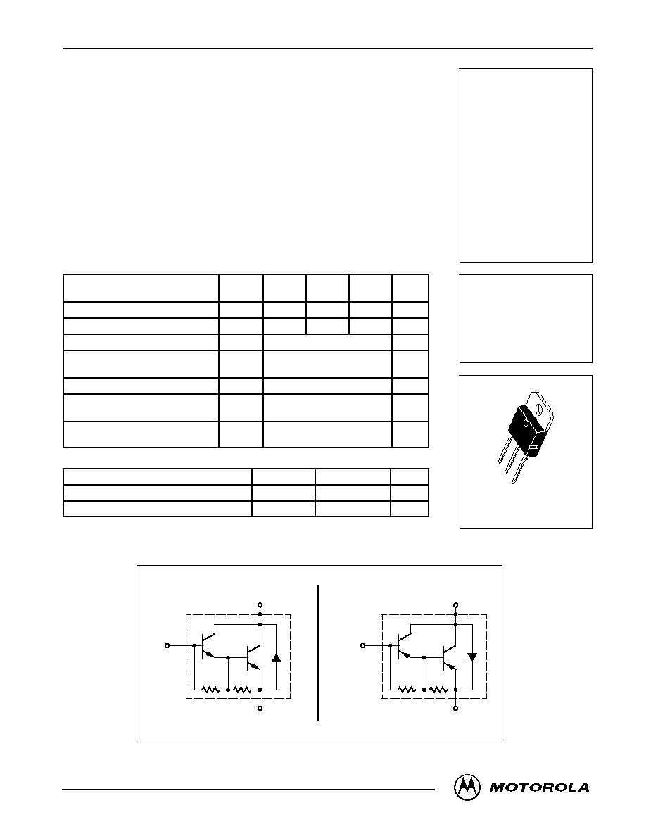
DARLINGTON SCHEMATICS
BASE
EMITTER
COLLECTOR
8.0 k
40
BASE
EMITTER
COLLECTOR
8.0 k
40
NPN
TIP140
TIP141
TIP142
PNP
TIP145
TIP146
TIP147
Preferred devices are Motorola recommended choices for future use and best overall value.
MOTOROLA
SEMICONDUCTOR TECHNICAL DATA
Order this document
by TIP140/D
©
Motorola, Inc. 1996
TIP140
TIP141
TIP142
TIP145
TIP146
TIP147
10 AMPERE
DARLINGTON
COMPLEMENTARY SILICON
POWER TRANSISTORS
60 ≠ 100 VOLTS
125 WATTS
*Motorola Preferred Device
*
NPN
PNP
*
*
*
CASE 340D≠02
REV 1

TIP140 TIP141 TIP142 TIP145 TIP146 TIP147
2
Motorola Bipolar Power Transistor Device Data
ŒŒŒŒŒŒŒŒŒŒŒŒŒŒŒŒŒŒŒŒŒŒŒŒŒŒŒŒŒŒŒŒŒŒ
ŒŒŒŒŒŒŒŒŒŒŒŒŒŒŒŒŒŒŒŒŒŒŒŒŒŒŒŒŒŒŒŒŒŒ
ELECTRICAL CHARACTERISTICS
(TC = 25
_
C unless otherwise noted)
ŒŒŒŒŒŒŒŒŒŒŒŒŒŒŒŒŒŒŒŒ
ŒŒŒŒŒŒŒŒŒŒŒŒŒŒŒŒŒŒŒŒ
Characteristic
ŒŒŒŒ
ŒŒŒŒ
Symbol
ŒŒŒŒ
ŒŒŒŒ
Min
ŒŒŒŒ
ŒŒŒŒ
Typ
ŒŒŒŒ
ŒŒŒŒ
Max
ŒŒŒ
ŒŒŒ
Unit
ŒŒŒŒŒŒŒŒŒŒŒŒŒŒŒŒŒŒŒŒŒŒŒŒŒŒŒŒŒŒŒŒŒŒ
ŒŒŒŒŒŒŒŒŒŒŒŒŒŒŒŒŒŒŒŒŒŒŒŒŒŒŒŒŒŒŒŒŒŒ
OFF CHARACTERISTICS
ŒŒŒŒŒŒŒŒŒŒŒŒŒŒŒŒŒŒŒŒ
Œ
ŒŒŒŒŒŒŒŒŒŒŒŒŒŒŒŒŒŒ
Œ
Œ
ŒŒŒŒŒŒŒŒŒŒŒŒŒŒŒŒŒŒ
Œ
ŒŒŒŒŒŒŒŒŒŒŒŒŒŒŒŒŒŒŒŒ
Collector≠Emitter Sustaining Voltage (1)
(IC = 30 mA, IB = 0)
TIP140, TIP145
TIP141, TIP146
TIP142, TIP147
ŒŒŒŒ
Œ
ŒŒ
Œ
Œ
ŒŒ
Œ
ŒŒŒŒ
VCEO(sus)
ŒŒŒŒ
Œ
ŒŒ
Œ
Œ
ŒŒ
Œ
ŒŒŒŒ
60
80
100
ŒŒŒŒ
Œ
ŒŒ
Œ
Œ
ŒŒ
Œ
ŒŒŒŒ
--
--
--
ŒŒŒŒ
Œ
ŒŒ
Œ
Œ
ŒŒ
Œ
ŒŒŒŒ
--
--
--
ŒŒŒ
ŒŒ
Œ
ŒŒ
Œ
ŒŒŒ
Vdc
ŒŒŒŒŒŒŒŒŒŒŒŒŒŒŒŒŒŒŒŒ
Œ
ŒŒŒŒŒŒŒŒŒŒŒŒŒŒŒŒŒŒ
Œ
Œ
ŒŒŒŒŒŒŒŒŒŒŒŒŒŒŒŒŒŒ
Œ
ŒŒŒŒŒŒŒŒŒŒŒŒŒŒŒŒŒŒŒŒ
Collector Cutoff Current
(VCE = 30 Vdc, IB = 0)
TIP140, TIP145
(VCE = 40 Vdc, IB = 0)
TIP141, TIP146
(VCE = 50 Vdc, IB = 0)
TIP142, TIP147
ŒŒŒŒ
Œ
ŒŒ
Œ
Œ
ŒŒ
Œ
ŒŒŒŒ
ICEO
ŒŒŒŒ
Œ
ŒŒ
Œ
Œ
ŒŒ
Œ
ŒŒŒŒ
--
--
--
ŒŒŒŒ
Œ
ŒŒ
Œ
Œ
ŒŒ
Œ
ŒŒŒŒ
--
--
--
ŒŒŒŒ
Œ
ŒŒ
Œ
Œ
ŒŒ
Œ
ŒŒŒŒ
2.0
2.0
2.0
ŒŒŒ
ŒŒ
Œ
ŒŒ
Œ
ŒŒŒ
mA
ŒŒŒŒŒŒŒŒŒŒŒŒŒŒŒŒŒŒŒŒ
Œ
ŒŒŒŒŒŒŒŒŒŒŒŒŒŒŒŒŒŒ
Œ
Œ
ŒŒŒŒŒŒŒŒŒŒŒŒŒŒŒŒŒŒ
Œ
ŒŒŒŒŒŒŒŒŒŒŒŒŒŒŒŒŒŒŒŒ
Collector Cutoff Current
(VCB = 60 V, IE = 0)
TIP140, TIP145
(VCB = 80 V, IE = 0)
TIP141, TIP146
(VCB = 100 V, IE = 0)
TIP142, TIP147
ŒŒŒŒ
Œ
ŒŒ
Œ
Œ
ŒŒ
Œ
ŒŒŒŒ
ICBO
ŒŒŒŒ
Œ
ŒŒ
Œ
Œ
ŒŒ
Œ
ŒŒŒŒ
--
--
--
ŒŒŒŒ
Œ
ŒŒ
Œ
Œ
ŒŒ
Œ
ŒŒŒŒ
--
--
--
ŒŒŒŒ
Œ
ŒŒ
Œ
Œ
ŒŒ
Œ
ŒŒŒŒ
1.0
1.0
1.0
ŒŒŒ
ŒŒ
Œ
ŒŒ
Œ
ŒŒŒ
mA
ŒŒŒŒŒŒŒŒŒŒŒŒŒŒŒŒŒŒŒŒ
ŒŒŒŒŒŒŒŒŒŒŒŒŒŒŒŒŒŒŒŒ
Emitter Cutoff Current (VBE = 5.0 V)
ŒŒŒŒ
ŒŒŒŒ
IEBO
ŒŒŒŒ
ŒŒŒŒ
--
ŒŒŒŒ
ŒŒŒŒ
--
ŒŒŒŒ
ŒŒŒŒ
2 0
ŒŒŒ
ŒŒŒ
mA
ŒŒŒŒŒŒŒŒŒŒŒŒŒŒŒŒŒŒŒŒŒŒŒŒŒŒŒŒŒŒŒŒŒŒ
ŒŒŒŒŒŒŒŒŒŒŒŒŒŒŒŒŒŒŒŒŒŒŒŒŒŒŒŒŒŒŒŒŒŒ
ON CHARACTERISTICS (1)
ŒŒŒŒŒŒŒŒŒŒŒŒŒŒŒŒŒŒŒŒ
Œ
ŒŒŒŒŒŒŒŒŒŒŒŒŒŒŒŒŒŒ
Œ
Œ
ŒŒŒŒŒŒŒŒŒŒŒŒŒŒŒŒŒŒ
Œ
ŒŒŒŒŒŒŒŒŒŒŒŒŒŒŒŒŒŒŒŒ
DC Current Gain
(IC = 5.0 A, VCE = 4.0 V)
(IC = 10 A, VCE = 4.0 V)
ŒŒŒŒ
Œ
ŒŒ
Œ
Œ
ŒŒ
Œ
ŒŒŒŒ
hFE
ŒŒŒŒ
Œ
ŒŒ
Œ
Œ
ŒŒ
Œ
ŒŒŒŒ
1000
500
ŒŒŒŒ
Œ
ŒŒ
Œ
Œ
ŒŒ
Œ
ŒŒŒŒ
--
--
ŒŒŒŒ
Œ
ŒŒ
Œ
Œ
ŒŒ
Œ
ŒŒŒŒ
--
--
ŒŒŒ
ŒŒ
Œ
ŒŒ
Œ
ŒŒŒ
--
ŒŒŒŒŒŒŒŒŒŒŒŒŒŒŒŒŒŒŒŒ
Œ
ŒŒŒŒŒŒŒŒŒŒŒŒŒŒŒŒŒŒ
Œ
ŒŒŒŒŒŒŒŒŒŒŒŒŒŒŒŒŒŒŒŒ
Collector≠Emitter Saturation Voltage
(IC = 5.0 A, IB = 10 mA)
(IC = 10 A, IB = 40 mA)
ŒŒŒŒ
Œ
ŒŒ
Œ
ŒŒŒŒ
VCE(sat)
ŒŒŒŒ
Œ
ŒŒ
Œ
ŒŒŒŒ
--
--
ŒŒŒŒ
Œ
ŒŒ
Œ
ŒŒŒŒ
--
--
ŒŒŒŒ
Œ
ŒŒ
Œ
ŒŒŒŒ
2.0
3.0
ŒŒŒ
ŒŒ
Œ
ŒŒŒ
Vdc
ŒŒŒŒŒŒŒŒŒŒŒŒŒŒŒŒŒŒŒŒ
Œ
ŒŒŒŒŒŒŒŒŒŒŒŒŒŒŒŒŒŒ
Œ
ŒŒŒŒŒŒŒŒŒŒŒŒŒŒŒŒŒŒŒŒ
Base≠Emitter Saturation Voltage
(IC = 10 A, IB = 40 mA)
ŒŒŒŒ
Œ
ŒŒ
Œ
ŒŒŒŒ
VBE(sat)
ŒŒŒŒ
Œ
ŒŒ
Œ
ŒŒŒŒ
--
ŒŒŒŒ
Œ
ŒŒ
Œ
ŒŒŒŒ
--
ŒŒŒŒ
Œ
ŒŒ
Œ
ŒŒŒŒ
3.5
ŒŒŒ
ŒŒ
Œ
ŒŒŒ
Vdc
ŒŒŒŒŒŒŒŒŒŒŒŒŒŒŒŒŒŒŒŒ
Œ
ŒŒŒŒŒŒŒŒŒŒŒŒŒŒŒŒŒŒ
Œ
ŒŒŒŒŒŒŒŒŒŒŒŒŒŒŒŒŒŒŒŒ
Base≠Emitter On Voltage
(IC = 10 A, VCE = 4.0 Vdc)
ŒŒŒŒ
Œ
ŒŒ
Œ
ŒŒŒŒ
VBE(on)
ŒŒŒŒ
Œ
ŒŒ
Œ
ŒŒŒŒ
--
ŒŒŒŒ
Œ
ŒŒ
Œ
ŒŒŒŒ
--
ŒŒŒŒ
Œ
ŒŒ
Œ
ŒŒŒŒ
3.0
ŒŒŒ
ŒŒ
Œ
ŒŒŒ
Vdc
ŒŒŒŒŒŒŒŒŒŒŒŒŒŒŒŒŒŒŒŒŒŒŒŒŒŒŒŒŒŒŒŒŒŒ
Œ
ŒŒŒŒŒŒŒŒŒŒŒŒŒŒŒŒŒŒŒŒŒŒŒŒŒŒŒŒŒŒŒŒ
Œ
SWITCHING CHARACTERISTICS
ŒŒŒŒŒŒŒŒŒŒŒŒŒŒŒŒŒŒŒŒŒŒŒŒŒŒŒŒŒŒŒŒŒŒ
Œ
ŒŒŒŒŒŒŒŒŒŒŒŒŒŒŒŒŒŒŒŒŒŒŒŒŒŒŒŒŒŒŒŒ
Œ
Resistive Load (See Figure 1)
ŒŒŒŒŒŒ
Œ
ŒŒŒŒ
Œ
Delay Time
ŒŒŒŒŒŒŒŒŒŒŒŒŒŒŒ
Œ
ŒŒŒŒŒŒŒŒŒŒŒŒŒ
Œ
(V
30 V I
5 0 A
ŒŒŒŒ
Œ
ŒŒ
Œ
td
ŒŒŒŒ
Œ
ŒŒ
Œ
--
ŒŒŒŒ
Œ
ŒŒ
Œ
0.15
ŒŒŒŒ
Œ
ŒŒ
Œ
--
ŒŒŒ
ŒŒ
Œ
µ
s
ŒŒŒŒŒŒ
Œ
ŒŒŒŒ
Œ
Rise Time
ŒŒŒŒŒŒŒŒŒŒŒŒŒŒŒ
Œ
ŒŒŒŒŒŒŒŒŒŒŒŒŒ
Œ
(VCC = 30 V, IC = 5.0 A,
IB = 20 mA Duty Cycle
v
2 0%
ŒŒŒŒ
Œ
ŒŒ
Œ
tr
ŒŒŒŒ
Œ
ŒŒ
Œ
--
ŒŒŒŒ
Œ
ŒŒ
Œ
0.55
ŒŒŒŒ
Œ
ŒŒ
Œ
--
ŒŒŒ
ŒŒ
Œ
µ
s
ŒŒŒŒŒŒ
Œ
ŒŒŒŒ
Œ
Storage Time
ŒŒŒŒŒŒŒŒŒŒŒŒŒŒŒ
Œ
ŒŒŒŒŒŒŒŒŒŒŒŒŒ
Œ
IB = 20 mA, Duty Cycle
v
2.0%,
IB1 = IB2, RC & RB Varied, TJ = 25
_
C)
ŒŒŒŒ
Œ
ŒŒ
Œ
ts
ŒŒŒŒ
Œ
ŒŒ
Œ
--
ŒŒŒŒ
Œ
ŒŒ
Œ
2.5
ŒŒŒŒ
Œ
ŒŒ
Œ
--
ŒŒŒ
ŒŒ
Œ
µ
s
ŒŒŒŒŒŒ
Œ
ŒŒŒŒ
Œ
Fall Time
ŒŒŒŒŒŒŒŒŒŒŒŒŒŒŒ
Œ
ŒŒŒŒŒŒŒŒŒŒŒŒŒ
Œ
B1
B2,
C
B
, J
)
ŒŒŒŒ
Œ
ŒŒ
Œ
tf
ŒŒŒŒ
Œ
ŒŒ
Œ
--
ŒŒŒŒ
Œ
ŒŒ
Œ
2.5
ŒŒŒŒ
Œ
ŒŒ
Œ
--
ŒŒŒ
ŒŒ
Œ
µ
s
(1) Pulse Test: Pulse Width = 300
µ
s, Duty Cycle
v
2.0%.
Figure 1. Switching Times Test Circuit
10
0.2
Figure 2. Switching Times
IC, COLLECTOR CURRENT (AMP)
t, TIME
(
s
)
µ
5.0
2.0
0.5
0.1
0.5
1.0
3.0
5.0
10
20
0.2
PNP
NPN
tf
tr
ts
td @ VBE(off) = 0
V2
approx
+12 V
V1
appox.
≠ 8.0 V
tr, tf
10 ns
DUTY CYCLE = 1.0%
25
µ
s
0
RB
51
D1
+ 4.0 V
VCC
≠ 30 V
RC
TUT
8.0 k
40
SCOPE
for td and tr, D1 is disconnected
and V2 = 0
RB & RC VARIED TO OBTAIN DESIRED CURRENT LEVELS
D1, MUST BE FAST RECOVERY TYPE, eg:
1N5825 USED ABOVE IB
100 mA
MSD6100 USED BELOW IB
100 mA
VCC = 30 V
IC/IB = 250
IB1 = IB2
TJ = 25
∞
C
For NPN test circuit reverse diode and voltage polarities.
1.0
TIP140 TIP141 TIP142 TIP145 TIP146 TIP147
3
Motorola Bipolar Power Transistor Device Data
V
CE(SA
T)
, COLLECT
OR≠EMITTER SA
TURA
TION
VOL
T
AGE (VOL
TS)
V
BE
, BASE≠EMITTER VOL
T
AGE (VOL
TS)
V
BE
, BASE≠EMITTER VOL
T
AGE (VOL
TS)
5000
0.5
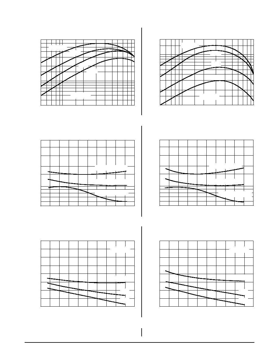
Figure 3. DC Current Gain versus Collector Current
IC, COLLECTOR CURRENT (AMPS)
300
1.0
2.0
3.0
5.0
7.0
10
500
h
FE
, DC CURRENT
GAIN
VCE = 4.0 V
4.0
NPN
TIP140, TIP141, TIP142
PNP
TIP145, TIP146, TIP147
Figure 4. Collector≠Emitter Saturation Voltage
5.0
≠ 75
TJ, JUNCTION TEMPERATURE (
∞
C)
0.5
IC = 10 A, IB = 4.0 mA
2.0
3.0
4.0
≠ 75
TJ, JUNCTION TEMPERATURE (
∞
C)
≠ 25
25
75
175
3.6
3.2
2.8
2.4
0.8
Figure 5. Base≠Emitter Voltage
2000
1000
TJ = 150
∞
C
25
∞
C
≠ 55
∞
C
IC, COLLECTOR CURRENT (AMPS)
h
FE
, DC CURRENT
GAIN
TJ, JUNCTION TEMPERATURE (
∞
C)
TJ, JUNCTION TEMPERATURE (
∞
C)
125
20,000
1000
2000
3000
5000
10,000
7000
1.0
0.7
0.5
V
CE(SA
T)
, COLLECT
OR≠EMITTER SA
TURA
TION
VOL
T
AGE (VOL
TS)
0.5
1.0
2.0
3.0
5.0
7.0
10
4.0
0.7
≠ 50
≠ 25
0
25
50
75
100
125
150
175
5.0
≠ 75
2.0
3.0
1.0
0.7
≠ 50
≠ 25
0
25
50
75
100
125
150
175
2.0
1.6
1.2
4.0
≠ 75
≠ 25
25
75
175
3.6
3.2
2.8
2.4
0.8
125
2.0
1.6
1.2
100
∞
C
TJ = 150
∞
C
100
∞
C
25
∞
C
≠ 55
∞
C
VCE = 4.0 V
IC = 5.0 A, IB = 10 mA
IC = 1.0 A, IB = 2.0 mA
IC = 10 A, IB = 4.0 mA
IC = 5.0 A, IB = 10 mA
IC = 1.0 A, IB = 2.0 mA
VCE = 4.0 V
IC = 10 A
5.0 A
1.0 A
VCE = 4.0 V
IC = 10 A
5.0 A
1.0 A
TYPICAL CHARACTERISTICS
TIP140 TIP141 TIP142 TIP145 TIP146 TIP147
4
Motorola Bipolar Power Transistor Device Data
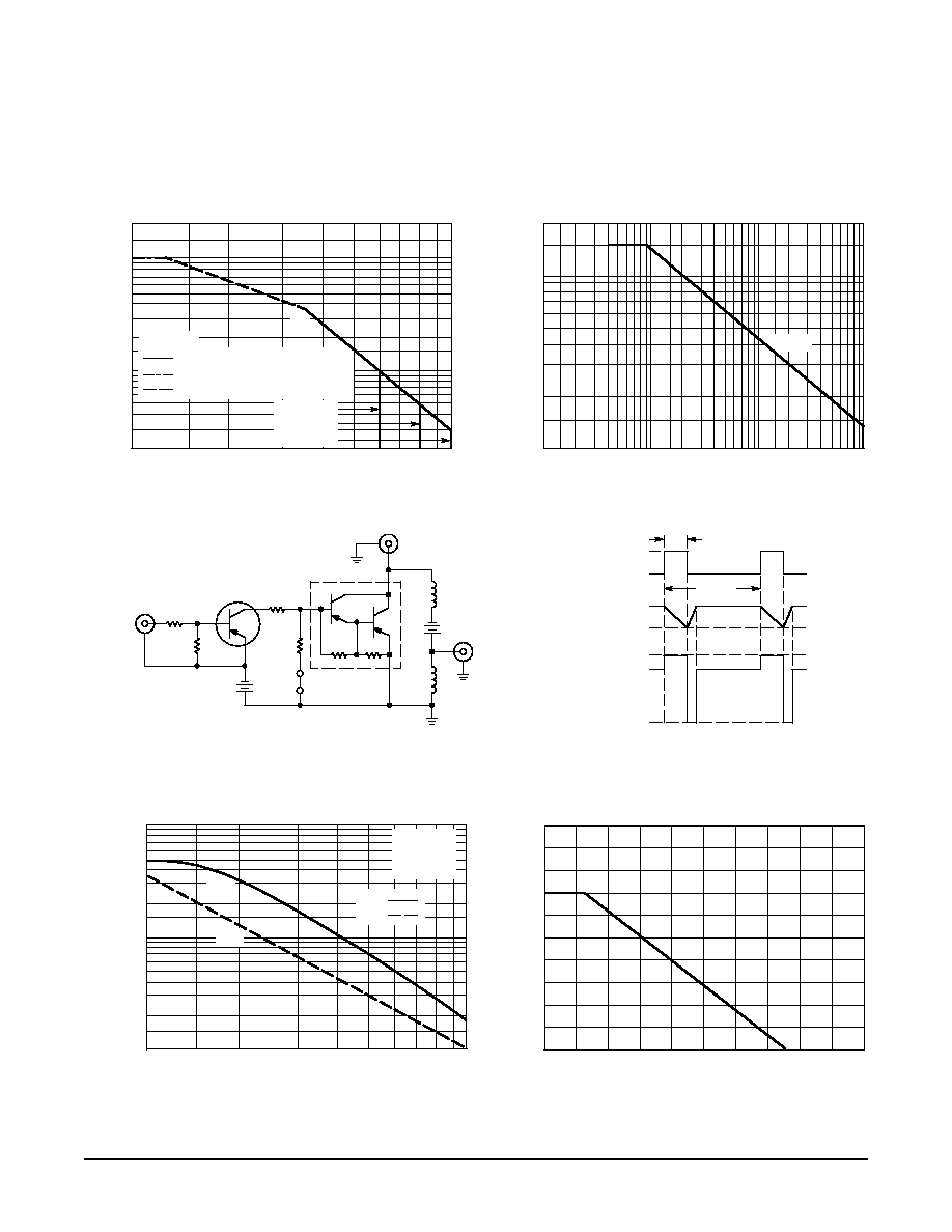
ACTIVE≠REGION SAFE OPERATING AREA
There are two limitations on the power handling ability of a
transistor: average junction temperature and second break-
down. Safe operating area curves indicate IC ≠ VCE limits of
the transistor that must be observed for reliable operation;
i.e., the transistor must not be subjected to greater dissipa-
tion than the curves indicate.
The data of Figure 6 is based on TJ(pk) = 150
_
C; TC is
variable depending on conditions. At high case temper-
atures, thermal limitations will reduce the power that can be
handled to values less than the limitations imposed by
second breakdown.
SECONDARY BREAKDOWN LIMIT
BONDING WIRE LIMIT
THERMAL LIMITATION @ TC = 25
∞
C
Figure 6. Active≠Region Safe Operating Area
dc
VCE, COLLECTOR≠EMITTER VOLTAGE (VOLTS)
2.0
I C
, COLLECT
OR
CURRENT
(AMP) (mA)
10
10
0.2
5.0
20
1.0
20
TJ = 150
∞
C
50
30
TIP140, 145
3.0
7.0
15
70
100
TIP141, 146
TIP142, 147
I C
, COLLECT
OR
CURRENT
(AMPS)
15
10
1.0
2.0
5.0
7.0
Figure 7. Unclamped Inductive Load
L, UNCLAMPED INDUCTIVE LOAD (mH)
0.5
1.0
2.0
5.0
10
20
50
100
100 mJ
INPUT
MPS≠U52
50
50
RBB1
1.5 k
RBB2
= 100
VBB2 = 0
VBB1 = 10 V
TUT
VCE MONITOR
100 mH
VCC = 20 V
IC
MONITOR
RS = 0.1
TEST CIRCUIT
NOTE 1: Input pulse width is increased until ICM = 1.42 A.
NOTE 2: For NPN test circuit reverse polarities.
INPUT
VOLTAGE
COLLECTOR
CURRENT
1.42 A
VCE(sat)
≠ 20 V
COLLECTOR
VOLTAGE
V(BR)CER
w
7.0 ms (SEE NOTE 1)
5.0 V
0
100 ms
0
VOLTAGE AND CURRENT WAVEFORMS
Figure 8. Inductive Load
P
D
, POWER DISSIP
A
TION (W
A
TTS)
PNP
NPN
Figure 9. Magnitude of Common Emitter
Small≠Signal Short≠Circuit Forward
Current Transfer Ratio
f, FREQUENCY (MHz)
2.0
1.0
10
5.0
100
1.0
3.0
5.0
7.0
2.0
7.0
10
VCE = 10 V
IC = 1.0 A
TJ = 25
∞
C
5.0
4.0
0
1.0
2.0
3.0
Figure 10. Free≠Air Temperature
Power Derating
TA, FREE≠AIR TEMPERATURE (
∞
C)
0
40
80
120
160
200
h
fe
, SMALL≠SIGNAL
FOR
W
ARD CURRENT
TRANSFER RA
TIO
20
50
70
PNP
NPN
TIP140 TIP141 TIP142 TIP145 TIP146 TIP147
5
Motorola Bipolar Power Transistor Device Data
PACKAGE DIMENSIONS
CASE 340D≠02
ISSUE B
NOTES:
1. DIMENSIONING AND TOLERANCING PER ANSI
Y14.5M, 1982.
2. CONTROLLING DIMENSION: MILLIMETER.
A
D
V
G
K
S
L
U
B
Q
E
C
J
H
DIM
MIN
MAX
MIN
MAX
INCHES
MILLIMETERS
A
≠≠≠
20.35
≠≠≠
0.801
B
14.70
15.20
0.579
0.598
C
4.70
4.90
0.185
0.193
D
1.10
1.30
0.043
0.051
E
1.17
1.37
0.046
0.054
G
5.40
5.55
0.213
0.219
H
2.00
3.00
0.079
0.118
J
0.50
0.78
0.020
0.031
K
31.00 REF
1.220 REF
L
≠≠≠
16.20
≠≠≠
0.638
Q
4.00
4.10
0.158
0.161
S
17.80
18.20
0.701
0.717
U
4.00 REF
0.157 REF
V
1.75 REF
0.069
1
2
3
4
STYLE 1:
PIN 1. BASE
2. COLLECTOR
3. EMITTER
4. COLLECTOR

TIP140 TIP141 TIP142 TIP145 TIP146 TIP147
6
Motorola Bipolar Power Transistor Device Data
Motorola reserves the right to make changes without further notice to any products herein. Motorola makes no warranty, representation or guarantee regarding
the suitability of its products for any particular purpose, nor does Motorola assume any liability arising out of the application or use of any product or circuit, and
specifically disclaims any and all liability, including without limitation consequential or incidental damages. "Typical" parameters which may be provided in Motorola
data sheets and/or specifications can and do vary in different applications and actual performance may vary over time. All operating parameters, including "Typicals"
must be validated for each customer application by customer's technical experts. Motorola does not convey any license under its patent rights nor the rights of
others. Motorola products are not designed, intended, or authorized for use as components in systems intended for surgical implant into the body, or other
applications intended to support or sustain life, or for any other application in which the failure of the Motorola product could create a situation where personal injury
or death may occur. Should Buyer purchase or use Motorola products for any such unintended or unauthorized application, Buyer shall indemnify and hold Motorola
and its officers, employees, subsidiaries, affiliates, and distributors harmless against all claims, costs, damages, and expenses, and reasonable attorney fees
arising out of, directly or indirectly, any claim of personal injury or death associated with such unintended or unauthorized use, even if such claim alleges that
Motorola was negligent regarding the design or manufacture of the part. Motorola and are registered trademarks of Motorola, Inc. Motorola, Inc. is an Equal
Opportunity/Affirmative Action Employer.
How to reach us:
USA / EUROPE / Locations Not Listed: Motorola Literature Distribution;
JAPAN: Nippon Motorola Ltd.; Tatsumi≠SPD≠JLDC, 6F Seibu≠Butsuryu≠Center,
P.O. Box 20912; Phoenix, Arizona 85036. 1≠800≠441≠2447 or 602≠303≠5454
3≠14≠2 Tatsumi Koto≠Ku, Tokyo 135, Japan. 03≠81≠3521≠8315
MFAX: RMFAX0@email.sps.mot.com ≠ TOUCHTONE 602≠244≠6609
ASIA/PACIFIC: Motorola Semiconductors H.K. Ltd.; 8B Tai Ping Industrial Park,
INTERNET: http://Design≠NET.com
51 Ting Kok Road, Tai Po, N.T., Hong Kong. 852≠26629298
TIP140/D
*TIP140/D*