©
Semiconductor Components Industries, LLC, 2001
October, 2001 ≠ Rev. 3
1
Publication Order Number:
UC3842A/D
UC3842A, UC3843A,
UC2842A, UC2843A
High Performance
Current Mode Controllers
The UC3842A, UC3843A series of high performance fixed
frequency current mode controllers are specifically designed for
off≠line and dc≠to≠dc converter applications offering the designer a
cost effective solution with minimal external components. These
integrated circuits feature a trimmed oscillator for precise duty cycle
control, a temperature compensated reference, high gain error
amplifier, current sensing comparator, and a high current totem pole
output ideally suited for driving a power MOSFET.
Also included are protective features consisting of input and
reference undervoltage lockouts each with hysteresis, cycle≠by≠cycle
current limiting, programmable output deadtime, and a latch for single
pulse metering.
These devices are available in an 8≠pin dual≠in≠line plastic package
as well as the 14≠pin plastic surface mount (SO≠14). The SO≠14
package has separate power and ground pins for the totem pole output
stage.
The UCX842A has UYLO thresholds of 16 V (on) and 10 V (off),
ideally suited for off≠line converters. The UCX843A is tailored for
lower voltage applications having UVLO thresholds of 8.5 V (on) and
7.6 V (off).
∑
Trimmed Oscillator Discharge Current for Precise Duty Cycle
Control
∑
Current Mode Operation to 500 kHz
∑
Automatic Feed Forward Compensation
∑
Latching PWM for Cycle≠By≠Cycle Current Limiting
∑
Internally Trimmed Reference with Undervoltage Lockout
∑
High Current Totem Pole Output
∑
Undervoltage Lockout with Hysteresis
∑
Low Startup and Operating Current
∑
Direct Interface with ON Semiconductor SENSEFET Products
http://onsemi.com
14
SO≠14
D SUFFIX
CASE 751A
1
See detailed ordering and shipping information in the package
dimensions section on page 15 of this data sheet.
ORDERING INFORMATION
See general marking information in the device marking
section on page 16 of this data sheet.
DEVICE MARKING INFORMATION
1
8
PDIP≠8
N SUFFIX
CASE 626
PIN CONNECTIONS
(Top View)
V
ref
(Top View)
Compensation
Voltage Feedback
Current Sense
R
T
/C
T
V
ref
V
CC
Output
Gnd
1
2
3
4
5
6
7
8
Compensation
NC
Voltage Feedback
NC
Current Sense
NC
R
T
/C
T
NC
V
CC
V
C
Output
Gnd
Power Ground
1
2
3
4
5
6
7
9
8
10
11
12
13
14
1
8
SO≠8
D1 SUFFIX
CASE 751
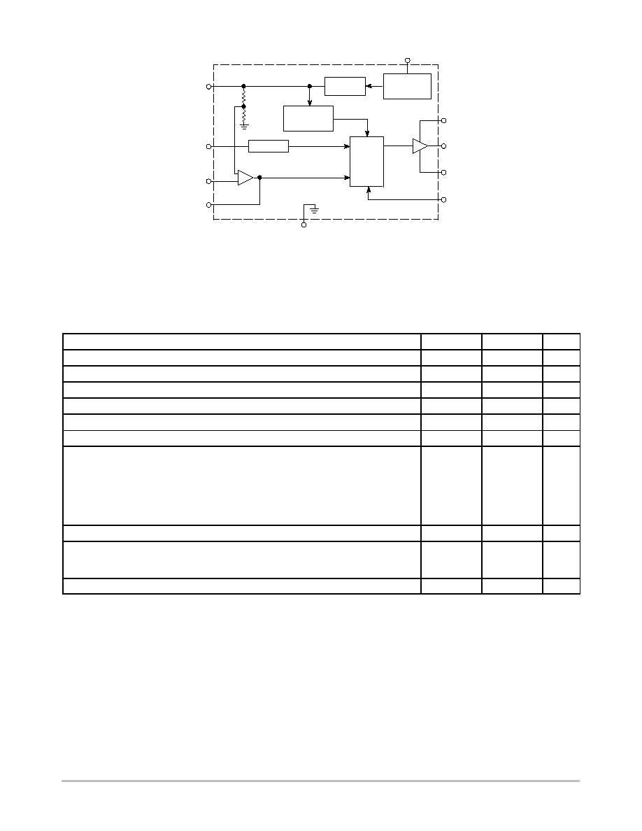
UC3842A, UC3843A, UC2842A, UC2843A
http://onsemi.com
2
Figure 1. Simplified Block Diagram
5.0V
Reference
Latching
PWM
V
CC
Undervoltage
Lockout
Oscillator
Error
Amplifier
7(12)
V
C
7(11)
Output
6(10)
Power
Ground
5(8)
3(5)
Current
Sense
Input
V
ref
8(14)
4(7)
2(3)
1(1)
Gnd
5(9)
R
T
C
T
Voltage
Feedback
Input
R
R
+
-
V
ref
Undervoltage
Lockout
Output
Compensation
Pin numbers in parenthesis are for the D suffix SO-14 package.
V
CC
MAXIMUM RATINGS
Rating
Symbol
Value
Unit
Bias and Driver Voltages (Zero Series Impedance, see also Total Device spec)
V
CC
, V
C
30
V
Total Power Supply and Zener Current
(I
CC
+ I
Z
)
30
mA
Output Current, Source or Sink (Note 1)
I
O
1.0
A
Output Energy (Capacitive Load per Cycle)
W
5.0
µ
J
Current Sense and Voltage Feedback Inputs
V
in
≠ 0.3 to + 5.5
V
Error Amp Output Sink Current
I
O
10
mA
Power Dissipation and Thermal Characteristics
D Suffix, Plastic Package
Maximum Power Dissipation @ T
A
= 25
∞
C
Thermal Resistance, Junction≠to≠Air
N Suffix, Plastic Package
Maximum Power Dissipation @ T
A
= 25
∞
C
Thermal Resistance, Junction≠to≠Air
P
D
R
JA
P
D
R
JA
862
145
1.25
100
mW
∞
C/W
W
∞
C/W
Operating Junction Temperature
T
J
+ 150
∞
C
Operating Ambient Temperature
UC3842A, UC3843A
UC2842A, UC2843A
T
A
0 to + 70
≠ 25 to + 85
∞
C
Storage Temperature Range
T
stg
≠ 65 to + 150
∞
C
1. Maximum Package power dissipation limits must be observed.

UC3842A, UC3843A, UC2842A, UC2843A
http://onsemi.com
3
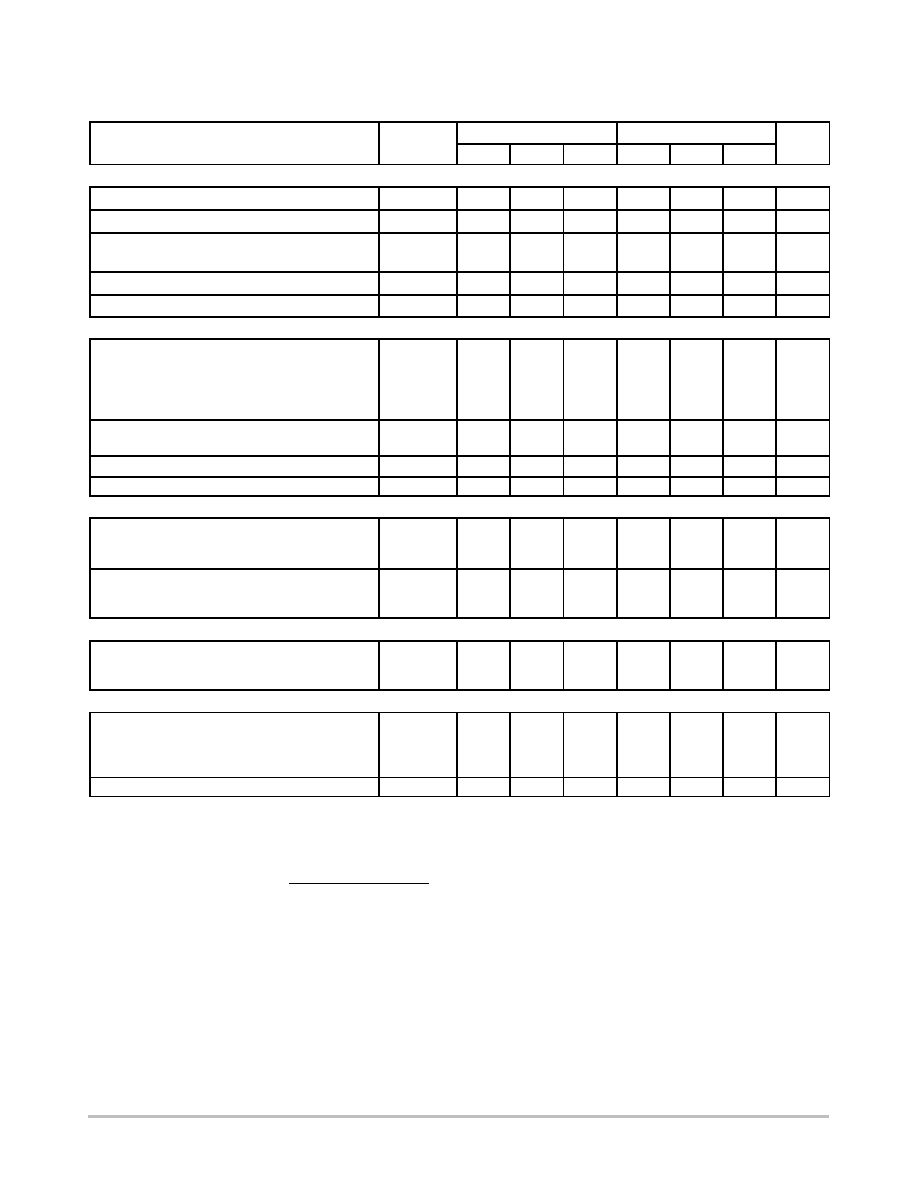
ELECTRICAL CHARACTERISTICS
(V
CC
= 15 V, [Note 2], R
T
= 10 k, C
T
= 3.3 nF, T
A
= T
low
to T
high
[Note 3],
unless otherwise noted.)
UC284XA
UC384XA
Characteristics
Symbol
Min
Typ
Max
Min
Typ
Max
Unit
REFERENCE SECTION
Reference Output Voltage (I
O
= 1.0 mA, T
J
= 25
∞
C)
V
ref
4.95
5.0
5.05
4.9
5.0
5.1
V
Line Regulation (V
CC
= 12 V to 25 V)
Reg
line
≠
2.0
20
≠
2.0
20
mV
Load Regulation (I
O
= 1.0 mA to 20 mA)
Reg
load
≠
3.0
25
≠
3.0
25
mV
Temperature Stability
T
S
≠
0.2
≠
≠
0.2
≠
mV/
∞
C
Total Output Variation over Line, Load, Temperature
V
ref
4.9
≠
5.1
4.82
≠
5.18
V
Output Noise Voltage (f = 10 Hz to 10 kHz,
T
J
= 25
∞
C)
V
n
≠
50
≠
≠
50
≠
µ
V
Long Term Stability (T
A
= 125
∞
C for 1000 Hours)
S
≠
5.0
≠
≠
5.0
≠
mV
Output Short Circuit Current
I
SC
≠ 30
≠ 85
≠ 180
≠ 30
≠ 85
≠ 180
mA
OSCILLATOR SECTION
Frequency
T
J
= 25
∞
C
T
A
= T
low
to T
high
f
osc
47
46
52
≠
57
60
47
46
52
≠
57
60
kHz
Frequency Change with Voltage (V
CC
= 12 V to 25 V)
f
osc/
V
≠
0.2
1.0
≠
0.2
1.0
%
Frequency Change with Temperature
T
A
= T
low
to T
high
f
osc/
T
≠
5.0
≠
≠
5.0
≠
%
Oscillator Voltage Swing (Peak≠to≠Peak)
V
osc
≠
1.6
≠
≠
1.6
≠
V
Discharge Current (V
osc
= 2.0 V)
T
J
= 25
∞
C
T
A
= T
low
to T
high
I
dischg
7.5
7.2
8.4
≠
9.3
9.5
7.5
7.2
8.4
≠
9.3
9.5
mA
ERROR AMPLIFIER SECTION
Voltage Feedback Input (V
O
= 2.5 V)
V
FB
2.45
2.5
2.55
2.42
2.5
2.58
V
Input Bias Current (V
FB
= 2.7 V)
I
IB
≠
≠0.1
≠1.0
≠
≠0.1
≠2.0
µ
A
Open Loop Voltage Gain (V
O
= 2.0 V to 4.0 V)
A
VOL
65
90
≠
65
90
≠
dB
Unity Gain Bandwidth (T
J
= 25
∞
C)
BW
0.7
1.0
≠
0.7
1.0
≠
MHz
Power Supply Rejection Ratio (V
CC
= 12 V to 25 V)
PSRR
60
70
≠
60
70
≠
dB
Output Current
Sink (V
O
= 1.1 V, V
FB
= 2.7 V)
Source (V
O
= 5.0 V, V
FB
= 2.3 V)
I
Sink
I
Source
2.0
≠0.5
12
≠1.0
≠
≠
2.0
≠0.5
12
≠1.0
≠
≠
mA
Output Voltage Swing
High State (R
L
= 15 k to ground, V
FB
= 2.3 V)
Low State (R
L
= 15 k to V
ref
, V
FB
= 2.7 V)
V
OH
V
OL
5.0
≠
6.2
0.8
≠
1.1
5.0
≠
6.2
0.8
≠
1.1
V
2. Adjust V
CC
above the Startup threshold before setting to 15 V.
3. Low duty cycle pulse techniques are used during test to maintain junction temperature as close to ambient as possible.
T
low
= 0
∞
C for UC3842A, UC3843A
T
high
= +70
∞
C for UC3842A, UC3843A
≠25
∞
C for UC2842A, UC2843A
+85
∞
C for UC2842A, UC2843A
UC3842A, UC3843A, UC2842A, UC2843A
http://onsemi.com
4
ELECTRICAL CHARACTERISTICS
(V
CC
= 15 V, [Note 4], R
T
= 10 k, C
T
= 3.3 nF, T
A
= T
low
to T
high
[Note 5],
unless otherwise noted.)
UC284XA
UC384XA
Characteristics
Symbol
Min
Typ
Max
Min
Typ
Max
Unit
CURRENT SENSE SECTION
Current Sense Input Voltage Gain (Notes 6 & 7)
A
V
2.85
3.0
3.15
2.85
3.0
3.15
V/V
Maximum Current Sense Input Threshold (Note 6)
V
th
0.9
1.0
1.1
0.9
1.0
1.1
V
Power Supply Rejection Ratio
V
CC
= 12 to 25 V (Note 6)
PSRR
≠
70
≠
≠
70
≠
dB
Input Bias Current
I
IB
≠
≠2.0
≠10
≠
≠2.0
≠10
µ
A
Propagation Delay (Current Sense Input to Output)
t
PLH(in/out)
≠
150
300
≠
150
300
ns
OUTPUT SECTION
Output Voltage
Low State (I
Sink
= 20 mA)
Low State
(I
Sink
= 200 mA)
High State (I
Sink
= 20 mA)
High State
(I
Sink
= 200 mA)
V
OL
V
OH
≠
≠
13
12
0.1
1.6
13.5
13.4
0.4
2.2
≠
≠
≠
≠
13
12
0.1
1.6
13.5
13.4
0.4
2.2
≠
≠
V
Output Voltage with UVLO Activated
V
CC
= 6.0 V, I
Sink
= 1.0 mA
V
OL(UVLO)
≠
0.1
1.1
≠
0.1
1.1
V
Output Voltage Rise Time (C
L
= 1.0 nF, T
J
= 25
∞
C)
t
r
≠
50
150
≠
50
150
ns
Output Voltage Fall Time (C
L
= 1.0 nF, T
J
= 25
∞
C)
t
f
≠
50
150
≠
50
150
ns
UNDERVOLTAGE LOCKOUT SECTION
Startup Threshold
UCX842A
UCX843A
V
th
15
7.8
16
8.4
17
9.0
14.5
7.8
16
8.4
17.5
9.0
V
Minimum Operating Voltage After Turn≠On
UCX842A
UCX843A
V
CC(min)
9.0
7.0
10
7.6
11
8.2
8.5
7.0
10
7.6
11.5
8.2
V
PWM SECTION
Duty Cycle
Maximum
Minimum
DC
max
DC
min
94
≠
96
≠
≠
0
94
≠
96
≠
≠
0
%
TOTAL DEVICE
Power Supply Current (Note 4)
Startup:
(V
CC
= 6.5 V for UCX843A,
(V
CC
=
14 V for UCX842A) Operating
I
CC
≠
≠
0.5
12
1.0
17
≠
≠
0.5
12
1.0
17
mA
Power Supply Zener Voltage (I
CC
= 25 mA)
V
Z
30
36
≠
30
36
≠
V
4. Adjust V
CC
above the Startup threshold before setting to 15 V.
5. Low duty cycle pulse techniques are used during test to maintain junction temperature as close to ambient as possible.
T
low
= 0
∞
C for UC3842A, UC3843A
T
high
= +70
∞
C for UC3842A, UC3843A
≠25
∞
C for UC2842A, UC2843A
+85
∞
C for UC2842A, UC2843A
6. This parameter is measured at the latch trip point with V
FB
= 0 V.
7. Comparator gain is defined as: A
V
V Output Compensation
V Current Sense Input
UC3842A, UC3843A, UC2842A, UC2843A
http://onsemi.com
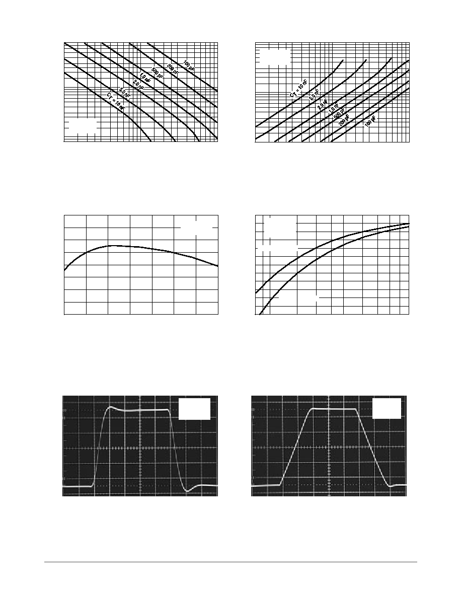
5
R T
,
TIMING RESIST
OR (k
)
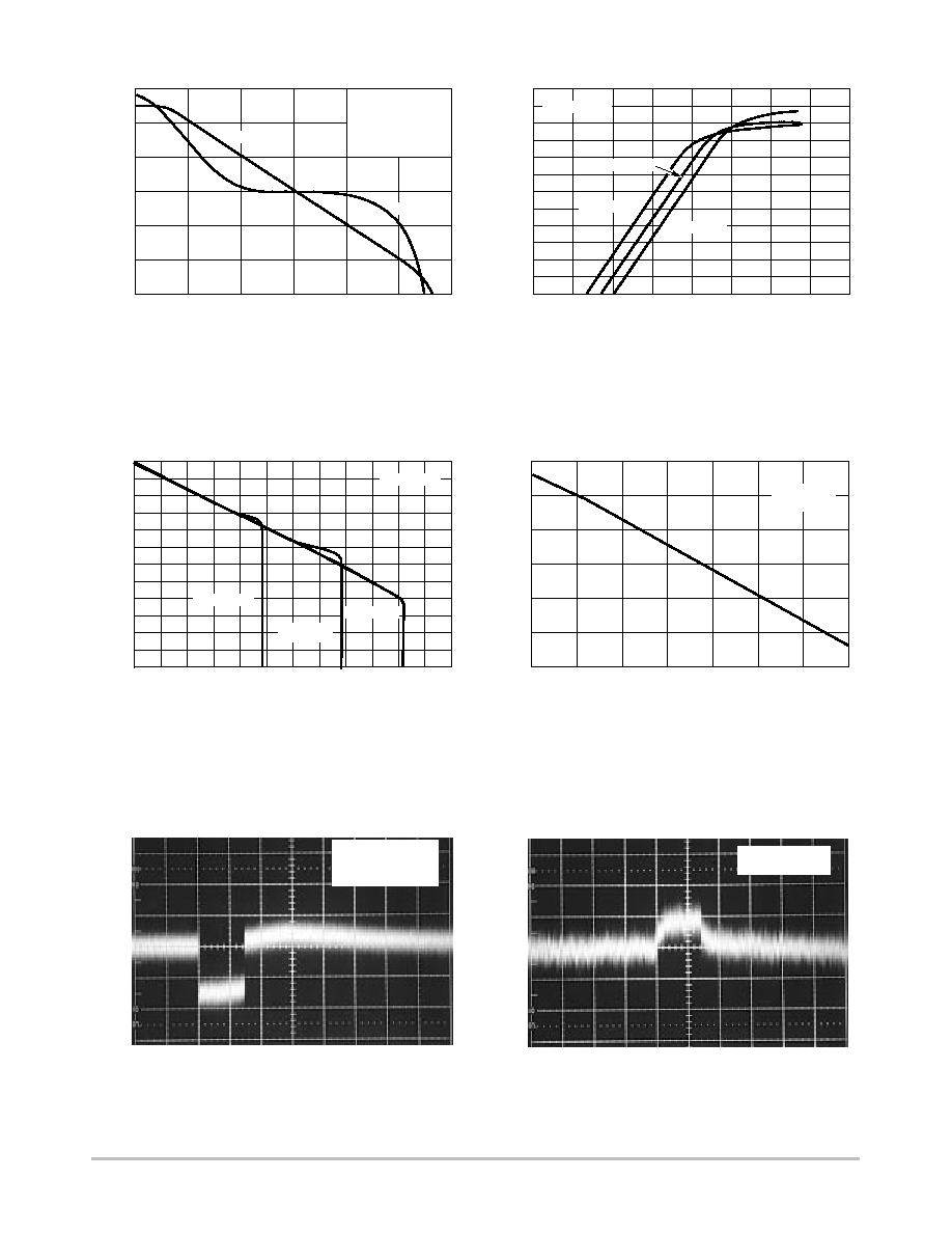
Figure 2. Timing Resistor versus
Oscillator Frequency
Figure 3. Output Deadtime versus
Oscillator Frequency
Figure 4. Oscillator Discharge Current
versus Temperature
Figure 5. Maximum Output Duty Cycle
versus Timing Resistor
Figure 6. Error Amp Small Signal
Transient Response
Figure 7. Error Amp Large Signal
Transient Response
0.5
µ
s/DIV
20 mV/DIV
V
CC
= 15 V
A
V
= -1.0
T
A
= 25
∞
C
10 k
20 k
50 k
100 k
200 k
500 k
1.0 M
f
OSC
, OSCILLATOR FREQUENCY (Hz)
V
CC
= 15 V
T
A
= 25
∞
C
10 k
20 k
50 k
100 k
200 k
500 k
1.0 M
f
OSC
, OSCILLATOR FREQUENCY (Hz)
% DT
, PERCENT
OUTPUT
DEADTIME
V
CC
= 15 V
T
A
= 25
∞
C
-55
-25
0
25
50
75
100
125
T
A
, AMBIENT TEMPERATURE (
∞
C)
, DISCHARGE CURRENT
(mA)
dischgI
V
CC
= 15 V
V
OSC
= 2.0 V
R
T
, TIMING RESISTOR (
)
800 1.0 k
2.0 k
3.0 k
4.0 k
6.0 k 8.0 k
, MAXIMUM OUTPUT
DUTY
CYCLE (%)
maxD
V
CC
= 15 V
C
T
= 3.3 nF
T
A
= 25
∞
C
I
dischg
= 9.5 mA
I
dischg
= 7.2 mA
2.55 V
2.5 V
2.45 V
V
CC
= 15 V
A
V
= -1.0
T
A
= 25
∞
C
0.1
µ
s/DIV
200 mV/DIV
2.5 V
3.0 V
2.0 V
80
50
20
8.0
5.0
2.0
0.8
100
50
20
10
5.0
2.0
1.0
9.0
8.5
8.0
7.5
7.0
100
90
80
70
60
50
40
UC3842A, UC3843A, UC2842A, UC2843A
http://onsemi.com
6
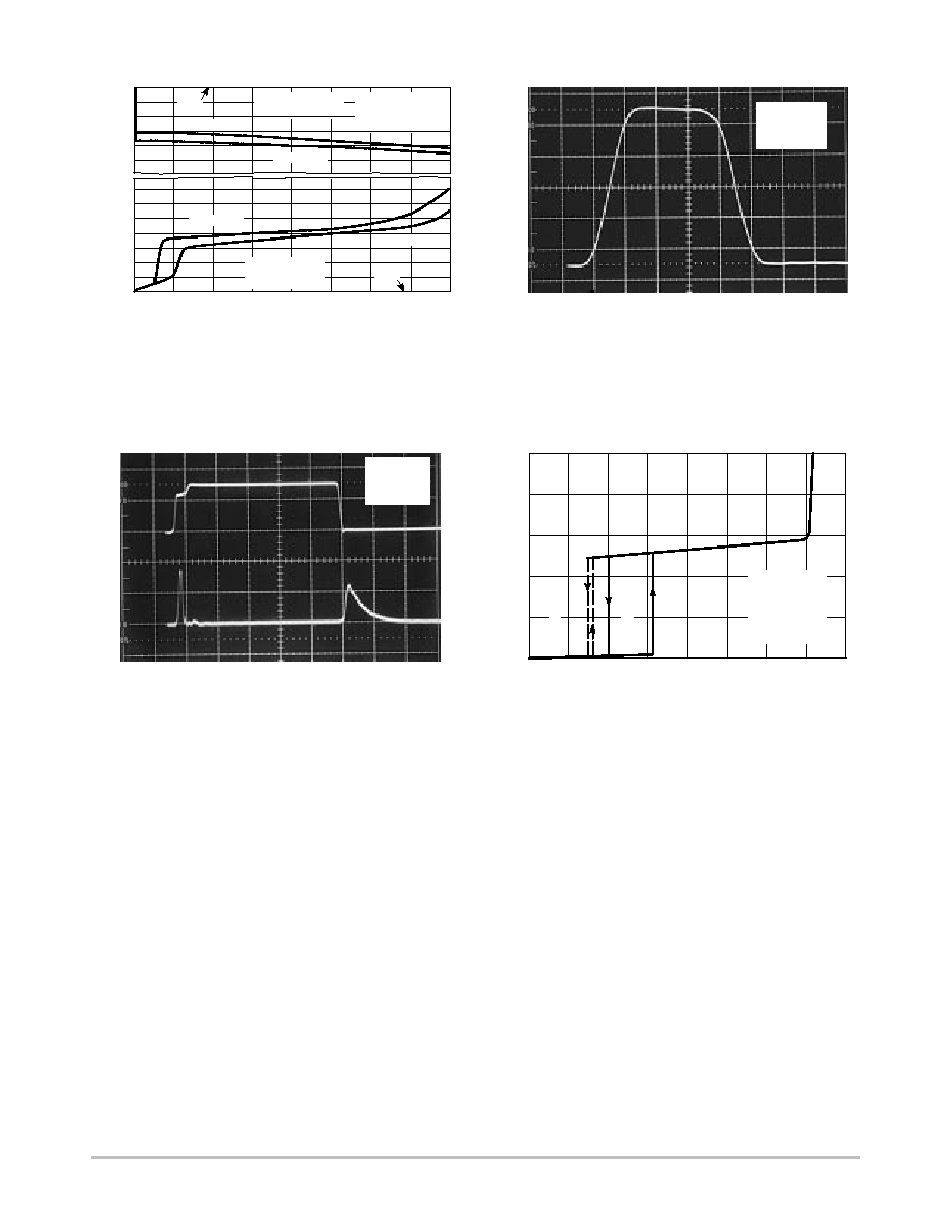
Figure 8. Error Amp Open Loop Gain and
Phase versus Frequency
Figure 9. Current Sense Input Threshold
versus Error Amp Output Voltage
Figure 10. Reference Voltage Change
versus Source Current
Figure 11. Reference Short Circuit Current
versus Temperature
Figure 12. Reference Load Regulation
Figure 13. Reference Line Regulation
, OUTPUT
VOL
T
AGE CHANGE (2.0 mV/DIV)
O
2.0 ms/DIV
V
, OUTPUT
VOL
T
AGE CHANGE (2.0 mV/DIV)
O
2.0 ms/DIV
V
V
CC
= 12 V to 25 V
T
A
= 25
∞
C
, REFERENCE VOL
T
AGE CHANGE (mV)
ref
0
20
40
60
80
100
120
I
ref
, REFERENCE SOURCE CURRENT (mA)
V
V
CC
= 15 V
T
A
= 55
∞
C
T
A
= 125
∞
C
, REFERENCE SHOR
T
CIRCUIT
CURRENT
(mA)
SC
-55
-25
0
25
50
75
100
125
T
A
, AMBIENT TEMPERATURE (
∞
C)
V
CC
= 15 V
R
L
0.1
I
V
CC
= 15 V
I
O
= 1.0 mA to 20 mA
T
A
= 25
∞
C
0
-4.0
-8.0
-12
-16
-20
-24
110
90
70
50
T
A
= 25
∞
C
- 20
A
VOL
, OPEN LOOP
VOL
T
AGE GAIN (dB)
10 M
10
f, FREQUENCY (Hz)
Gain
Phase
V
CC
= 15 V
V
O
= 2.0 V to 4.0 V
R
L
= 100 K
T
A
= 25
∞
C
0
30
60
90
120
150
180
100
1.0 k
10 k
100 k
1.0 M
0
20
40
60
80
100
, EXCESS PHASE (DEGREES)
0
V
O
, ERROR AMP OUTPUT VOLTAGE (V)
0
, CURRENT
SENSE INPUT
THRESHOLD (V
)
V th
0.2
0.4
0.6
0.8
1.0
1.2
2.0
4.0
6.0
8.0
V
CC
= 15 V
T
A
= 25
∞
C
T
A
= -55
∞
C
T
A
= 125
∞
C
UC3842A, UC3843A, UC2842A, UC2843A
http://onsemi.com
7
Figure 14. Output Saturation Voltage
versus Load Current
Figure 15. Output Waveform
Figure 16. Output Cross Conduction
Figure 17. Supply Current versus
Supply Voltage
50 ns/DIV
V
CC
= 15 V
C
L
= 1.0 nF
T
A
= 25
∞
C
100 ns/DIV
V
CC
= 30 V
C
L
= 15 pF
T
A
= 25
∞
C
, SUPPL
Y
CURRENT
100 mA/DIV
20 V/DIV
I
, OUTPUT
VOL
T
AGE
V
CC
O
800
600
400
200
0
I
O
, OUTPUT LOAD CURRENT (mA)
, OUTPUT
SA
TURA
TION VOL
T
AGE (V)
satV
V
CC
T
A
= 25
∞
C
T
A
= -55
∞
C
Gnd
T
A
= 25
∞
C
Source Saturation
(Load to Ground)
T
A
= -55
∞
C
V
CC
= 15 V
80
µ
s Pulsed Load
120 Hz Rate
0
10
20
30
40
, SUPPL
Y
CURRENT
(mA)
CC
V
CC
, SUPPLY VOLTAGE
I
R
T
= 10 k
C
T
= 3.3 nF
V
FB
= 0 V
I
Sense
= 0 V
T
A
= 25
∞
C
UCX843A
UCX842A
90%
10%
0
1.0
2.0
3.0
-2.0
-1.0
0
25
20
15
10
5
0
Sink Saturation
(Load to V
CC
)

UC3842A, UC3843A, UC2842A, UC2843A
http://onsemi.com
8
+
-
Sink Only
Positive True Logic
=
R
S
+
Internal
Bias
Reference
Regulator
Oscillator
S
R
Q
-
V
ref
UVLO
3.6V
36V
V
CC
7(12)
Q1
V
in
V
CC
V
C
7(11)
6(10)
5(8)
3(5)
+
1.0mA
Error
Amplifier
1(1)
2(3)
4(7)
8(14)
5(9)
Gnd
Output
Compensation
Voltage Feedback
Input
R
T
C
T
V
ref
-
-
PWM
Latch
Current Sense
Comparator
R
R
Power Ground
Current Sense Input
2R
R
1.0V
Pin numbers in parenthesis are for the D suffix SO-14 package.
Q
T
+
-
+
+
-
+
-
+
V
CC
UVLO
Output
2.5V
Figure 18. Representative Block Diagram
Output/
Compensation
Current Sense
Input
Latch
``Reset'' Input
Output
Capacitor C
T
Latch
``Set'' Input
Large R
T
/Small C
T
Small R
T
/Large C
T
Figure 19. Timing Diagram

UC3842A, UC3843A, UC2842A, UC2843A
http://onsemi.com
9
OPERATING DESCRIPTION
The UC3842A, UC3843A series are high performance,
fixed frequency, current mode controllers. They are
specifically designed for Off≠Line and dc≠to≠dc converter
applications offering the designer a cost effective solution
with minimal external components. A representative block
diagram is shown in Figure 18.
Oscillator
The oscillator frequency is programmed by the values
selected for the timing components R
T
and C
T
. Capacitor C
T
is charged from the 5.0 V reference through resistor R
T
to
approximately 2.8 V and discharged to 1.2 V by an internal
current sink. During the discharge of C
T
, the oscillator
generates and internal blanking pulse that holds the center
input of the NOR gate high. This causes the Output to be in
a low state, thus producing a controlled amount of output
deadtime. Figure 2 shows R
T
versus Oscillator Frequency
and Figure 3, Output Deadtime versus Frequency, both for
given values of C
T
. Note that many values of R
T
and C
T
will
give the same oscillator frequency but only one combination
will yield a specific output deadtime at a given frequency.
The oscillator thresholds are temperature compensated, and
the discharge current is trimmed and guaranteed to within
±
10% at T
J
= 25
∞
C. These internal circuit refinements
minimize variations of oscillator frequency and maximum
output duty cycle. The results are shown in Figures 4 and 5.
In many noise sensitive applications it may be desirable to
frequency≠lock the converter to an external system clock.
This can be accomplished by applying a clock signal to the
circuit shown in Figure 21. For reliable locking, the
free≠running oscillator frequency should be set about 10%
less than the clock frequency. A method for multi unit
synchronization is shown in Figure 22. By tailoring the
clock waveform, accurate Output duty cycle clamping can
be achieved.
Error Amplifier
A fully compensated Error Amplifier with access to the
inverting input and output is provided. It features a typical
dc voltage gain of 90 dB, and a unity gain bandwidth of
1.0 MHz with 57 degrees of phase margin (Figure 8). The
noninverting input is internally biased at 2.5 V and is not
pinned out. The converter output voltage is typically divided
down and monitored by the inverting input. The maximum
input bias current is ≠2.0
µ
A which can cause an output
voltage error that is equal to the product of the input bias
current and the equivalent input divider source resistance.
The Error Amp Output (Pin 1) is provide for external loop
compensation (Figure 31). The output voltage is offset by
two diode drops (
1.4 V) and divided by three before it
connects to the inverting input of the Current Sense
Comparator. This guarantees that no drive pulses appear at
the Output (Pin 6) when Pin 1 is at its lowest state (V
OL
).
This occurs when the power supply is operating and the load
is removed, or at the beginning of a soft≠start interval
(Figures 24, 25). The Error Amp minimum feedback
resistance is limited by the amplifier's source current
(0.5 mA) and the required output voltage (V
OH
) to reach the
comparator's 1.0 V clamp level:
R
f(min)
3.0 (1.0 V) + 1.4 V
0.5 mA
= 8800
Current Sense Comparator and PWM Latch
The UC3842A, UC3843A operate as a current mode
controller, whereby output switch conduction is initiated by
the oscillator and terminated when the peak inductor current
reaches the threshold level established by the Error
Amplifier Output/Compensation (Pin1). Thus the error
signal controls the peak inductor current on a
cycle≠by≠cycle basis. The current Sense Comparator PWM
Latch configuration used ensures that only a single pulse
appears at the Output during any given oscillator cycle. The
inductor current is converted to a voltage by inserting the
ground referenced sense resistor R
S
in series with the source
of output switch Q1. This voltage is monitored by the
Current Sense Input (Pin 3) and compared a level derived
from the Error Amp Output. The peak inductor current under
normal operating conditions is controlled by the voltage at
pin 1 where:
I
pk
=
V
(Pin 1)
≠ 1.4 V
3 R
S
Abnormal operating conditions occur when the power
supply output is overloaded or if output voltage sensing is
lost. Under these conditions, the Current Sense Comparator
threshold will be internally clamped to 1.0 V. Therefore the
maximum peak switch current is:
I
pk(max)
=
1.0 V
R
S
When designing a high power switching regulator it
becomes desirable to reduce the internal clamp voltage in
order to keep the power dissipation of R
S
to a reasonable
level. A simple method to adjust this voltage is shown in
Figure 23. The two external diodes are used to compensate
the internal diodes yielding a constant clamp voltage over
temperature. Erratic operation due to noise pickup can result
if there is an excessive reduction of the I
pk(max)
clamp
voltage.
A narrow spike on the leading edge of the current
waveform can usually be observed and may cause the power
supply to exhibit an instability when the output is lightly
loaded. This spike is due to the power transformer
interwinding capacitance and output rectifier recovery time.
The addition of an RC filter on the Current Sense Input with
a time constant that approximates the spike duration will
usually eliminate the instability; refer to Figure 27.

UC3842A, UC3843A, UC2842A, UC2843A
http://onsemi.com
10
PIN FUNCTION DESCRIPTION
Pin
8≠Pin
14≠Pin
Function
Description
1
1
Compensation
This pin is Error Amplifier output and is made available for loop compensation.
2
3
Voltage
Feedback
This is the inverting input of the Error Amplifier. It is normally connected to the switching
power supply output through a resistor divider.
3
5
Current Sense
A voltage proportional to inductor current is connected to this input. The PWM uses this
information to terminate the output switch conduction.
4
7
R
T
/C
T
The Oscillator frequency and maximum Output duty cycle are programmed by connecting
resistor R
T
to V
ref
and capacitor C
T
to ground. Operation to 500 kHz is possible.
5
≠
Gnd
This pin is the combined control circuitry and power ground (8≠pin package only).
6
10
Output
This output directly drives the gate of a power MOSFET. Peak currents up to 1.0 A are
sourced and sunk by this pin.
7
12
V
CC
This pin is the positive supply of the control IC.
8
14
V
ref
This is the reference output. It provides charging current for capacitor C
T
through
resistor R
T
.
≠
8
Power Ground
This pin is a separate power ground return (14≠pin package only) that is connected back
to the power source. It is used to reduce the effects of switching transient noise on the
control circuitry.
≠
11
V
C
The Output high state (V
OH
) is set by the voltage applied to this pin (14≠pin package only).
With a separate power source connection, it can reduce the effects of switching transient
noise on the control circuitry.
≠
9
Gnd
This pin is the control circuitry ground return (14≠pin package only) and is connected back to
the power source ground.
≠
2,4,6,13
NC
No connection (14≠pin package only). These pins are not internally connected.
Undervoltage Lockout
Two undervoltage lockout comparators have been
incorporated to guarantee that the IC is fully functional
before the output stage is enabled. The positive power
supply terminal (V
CC
) and the reference output (V
ref
) are
each monitored by separate comparators. Each has built≠in
hysteresis to prevent erratic output behavior as their
respective thresholds are crossed. The V
CC
comparator
upper and lower thresholds are 16 V/10 V for the UCX842A,
and 8.4 V/7.6 V for the UCX843A. The V
ref
comparator
upper and lower thresholds are 3.6V/3.4 V. The large
hysteresis and low startup current of the UCX842A makes
it ideally suited in off≠line converter applications where
efficient bootstrap startup techniques are required
(Figure 34). The UCX843A is intended for lower voltage dc
to dc converter applications. A 36 V zener is connected as
a shunt regulator form V
CC
to ground. Its purpose is to
protect the IC from excessive voltage that can occur during
system startup. The minimum operating voltage for the
UCX842A is 11 V and 8.2 V for the UCX843A.
Output
These devices contain a single totem pole output stage that
was specifically designed for direct drive of power
MOSFETs. It is capable of up to
±
1.0 A peak drive current
and has a typical rise and fall time of 50 ns with a 1.0 nF load.
Additional internal circuitry has been added to keep the
Output in a sinking mode whenever an undervoltage lockout
is active. This characteristic eliminates the need for an
external pull≠down resistor.
The SO≠14 surface mount package provides separate pins
for V
C
(output supply) and Power Ground. Proper
implementation will significantly reduce the level of
switching transient noise imposed on the control circuitry.
This becomes particularly useful when reducing the I
pk(max)
clamp level. The separate V
C
supply input allows the
designer added flexibility in tailoring the drive voltage
independent of V
CC
. A zener clamp is typically connected
to this input when driving power MOSFETs in systems
where V
CC
is greater than 20 V. Figure 26 shows proper
power and control ground connections in a current sensing
power MOSFET application.
Reference
The 5.0 V bandgap reference is trimmed to
±
1.0%
tolerance at T
J
= 25
∞
C on the UC284XA, and
±
2.0% on the
UC384XA. Its primary purpose is to supply charging current
to the oscillator timing capacitor. The reference has short
circuit protection and is capable of providing in excess of
20 mA for powering additional control system circuitry.
UC3842A, UC3843A, UC2842A, UC2843A
http://onsemi.com
11
DESIGN CONSIDERATIONS
Do not attempt to construct the converter on
wire≠wrap or plug≠in prototype boards. High Frequency
circuit layout techniques are imperative to prevent
pulsewidth jitter. This is usually caused by excessive noise
pick≠up imposed on the Current Sense or Voltage Feedback
inputs. Noise immunity can be improved by lowering circuit
impedances at these points. The printed circuit layout should
contain a ground plane with low≠current signal and
high≠current switch and output grounds returning on
separate paths back to the input filter capacitor. Ceramic
bypass capacitors (0.1
µ
F) connected directly to V
CC
, V
C
,
and V
ref
may be required depending upon circuit layout.
This provides a low impedance path for filtering the high
frequency noise. All high current loops should be kept as
short as possible using heavy copper runs to minimize
radiated EMI. The Error Amp compensation circuitry and
the converter output voltage divider should be located close
to the IC and as far as possible from the power switch and
other noise generating components.
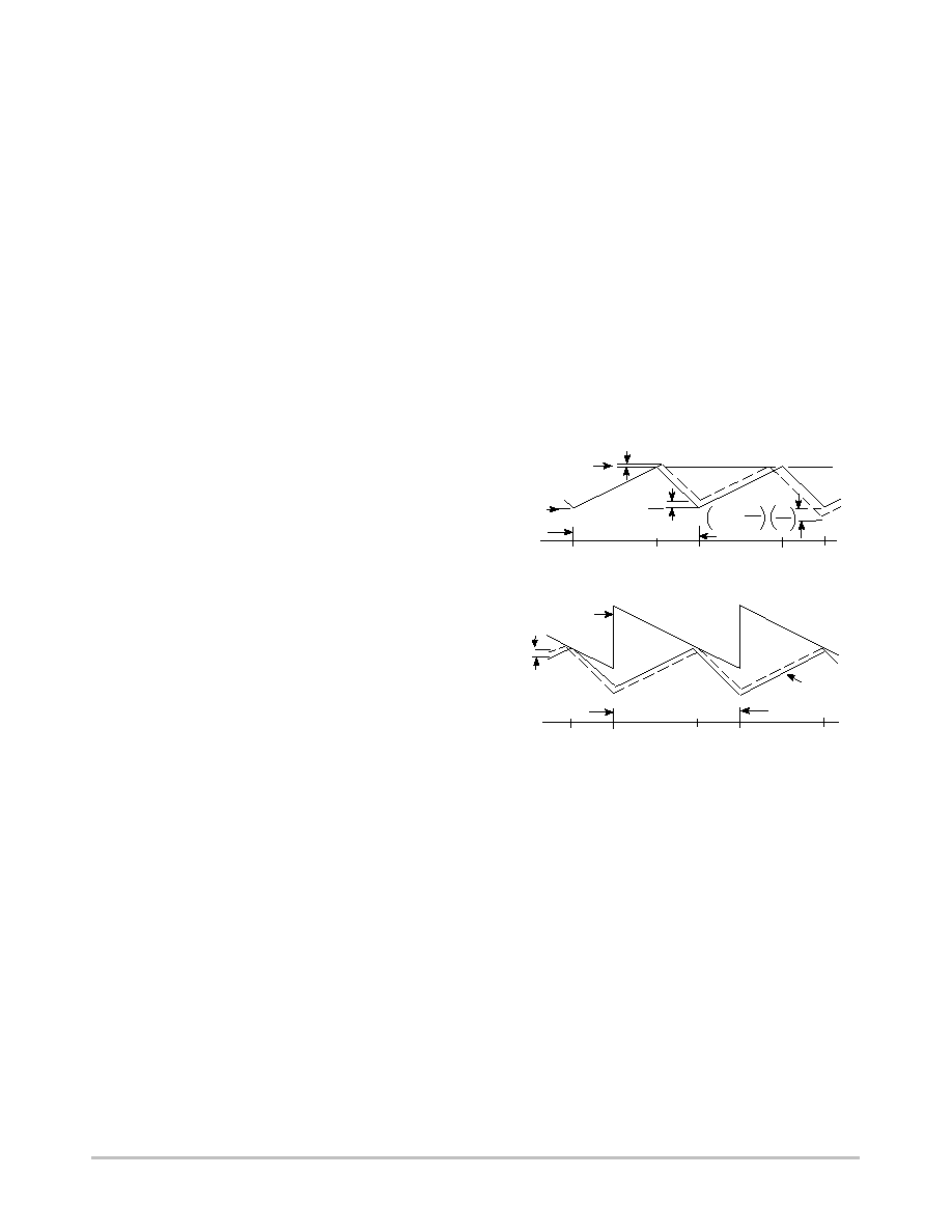
Current mode converters can exhibit subharmonic
oscillations when operating at a duty cycle greater than 50%
with continuous inductor current. This instability is
independent of the regulators closed≠loop characteristics
and is caused by the simultaneous operating conditions of
fixed frequency and peak current detecting. Figure 20A
shows the phenomenon graphically. At t
0
, switch
conduction begins, causing the inductor current to rise at a
slope of m
1
. This slope is a function of the input voltage
divided by the inductance. At t
1
, the Current Sense Input
reaches the threshold established by the control voltage.
This causes the switch to turn off and the current to decay at
a slope of m
2
until the next oscillator cycle. The unstable
condition can be shown if a pertubation is added to the
control voltage, resulting in a small
I (dashed line). With
a fixed oscillator period, the current decay time is reduced,
and the minimum current at switch turn≠on (t
2
) is increased
by
I +
I m2/m1. The minimum current at the next cycle
(t
3
) decreases to (
I +
I m
2
/m
1
) (m
2
/m
1
). This pertubation
is multiplied by m
2
.m
1
on each succeeding cycle, alternately
increasing and decreasing the inductor current at switch
turn≠on. Several oscillator cycles may be required before
the inductor current reaches zero causing the process to
commence again. If m
2
/m
1
is greater than 1, the converter
will be unstable. Figure 20B shows that by adding an
artificial ramp that is synchronized with the PWM clock to
the control voltage, the
I pertubation will decrease to zero
on succeeding cycles. This compensation ramp (m
3
) must
have a slope equal to or slightly greater than m
2
/2 for
stability. With m
2
/2 slope compensation, the average
inductor current follows the control voltage yielding true
current mode operation. The compensating ramp can be
derived from the oscillator and added to either the Voltage
Feedback or Current Sense inputs (Figure 33).
Figure 20. Continuous Current Waveforms
(A)
(B)
t
0
t
1
t
2
t
3
t
4
t
5
t
6
Control Voltage
I
m1
m2
m3
m1
m2
Oscillator Period
Oscillator Period
Control Voltage
I
Inductor
Current
I +
I
m
2
m
1
m
2
m
1
I +
I m
2
m
1
Inductor
Current
UC3842A, UC3843A, UC2842A, UC2843A
http://onsemi.com
12
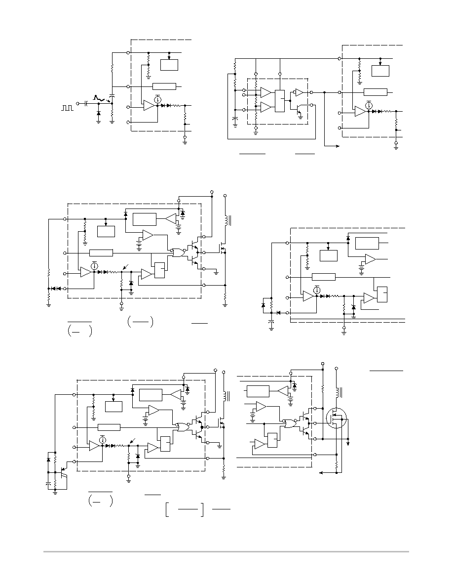
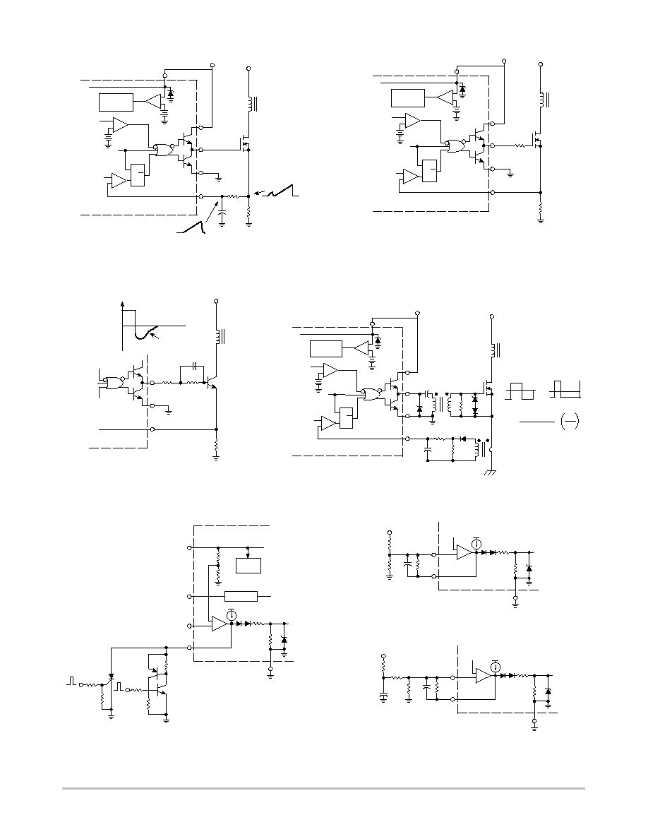
Figure 21. External Clock Synchronization
Figure 22. External Duty Cycle Clamp and
Multi Unit Synchronization
Figure 23. Adjustable Reduction of Clamp Level
Figure 24. Soft≠Start Circuit
Figure 25. Adjustable Buffered Reduction of
Clamp Level with Soft≠Start
Figure 26. Current Sensing Power MOSFET
Virtually lossless current sensing can be achieved with the implementation of a
SENSEFET power switch. For proper operation during over current conditions, a
reduction of the I
pk(max)
clamp level must be implemented. Refer to Figures 23 and 25.
The diode clamp is required if the Sync amplitude is large enough to
cause the bottom side of CT to go more than 300 mV below ground.
External
Sync
Input
47
5(9)
R
R
Bias
Osc
V
ref
R
T
8(14)
4(7)
2(3)
1(1)
0.01
C
T
2R
R
EA
+
-
+
5(9)
R
R
Bias
Osc
8(14)
4(7)
2(3)
1(1)
2R
R
EA
+
-
+
7
5.0k
3
8
6
5
1
C
R
S
MC1455
2
R
A
+
-
+
-
4
Q
5.0k
5.0k
R
B
To
Additional
UCX84XA's
f =
1.44
(R
A
+ 2R
B
)C
D
max
=
R
B
R
A
+ 2R
B
5(9)
R
R
Bias
Osc
8(14)
4(7)
2(3)
1(1)
2R
R
EA
+
-
+
Q1
R
S
3(5)
5(8)
1.0V
-
R
S
Q
Comp/Latch
5.0V
ref
V
Clamp
V
in
V
CC
7(11)
6(10)
-
+
+
-
+
- +
7(12)
+
-
R
1
R
2
R
2
V
Clamp
=
1.67
+ 1
+ 0.33 x 10 - 3
I
pk(max)
=
VClamp
RS
Where: 0
V
Clamp
1.0 V
R2
R1
1.0mA
R
1
R
1
+ R
2
5(9)
R
R
Bias
Osc
8(14)
4(7)
2(3)
1(1)
2R
R
EA
+
-
+
1.0V
-
R
S
Q
5.0V
ref
-
+
+
-
+
C
t
Soft-Start
3600C in
µ
F
1.0M
1.0mA
5(9)
R
R
Bias
Osc
8(14)
4(7)
2(3)
1(1)
2R
R
EA
+
-
+
Q1
R
S
3(5)
5(8)
1.0V
-
R
S
Q
Comp/Latch
5.0V
ref
V
Clamp
V
in
V
CC
7(11)
6(10)
-
+
+
-
+
- +
7(12)
+
-
MPSA63
R1
R2
C
t
Softstart
= - In
1 -
V
C
R
1
R
2
C
R
2
V
Clamp
=
1.67
+ 1
I
pk(max)
=
VClamp
RS
Where: 0
V
Clamp
1.0 V
1.0mA
R
1
3V
Clamp
R
1
+ R
2
R
S
1/4 W
(5)
(8)
-
R
S
Q
Comp/Latch
5.0V
ref
V
in
V
CC
(11)
(10)
-
+
+
-
+
- +
(12)
+
-
Power Ground
To Input Source
Return
V
Pin
5 =
If: SENSEFET = MTP10N10M
R
S
= 200
Then: V
pin
5 = 0.075 I
pk
SENSEFET
R
S
I
pk
r
DS(on)
M
G
D
S
K
Control CIrcuitry
Ground:
To Pin (9)
r
DM(on)
+ R
S
UC3842A, UC3843A, UC2842A, UC2843A
http://onsemi.com
13
Figure 27. Current Waveform Spike Suppression
Figure 28. MOSFET Parasitic Oscillations
Figure 29. Bipolar Transistor Drive
Figure 30. Isolated MOSFET Drive
Figure 31. Latched Shutdown
Figure 32. Error Amplifier Compensation
The totem-pole output can furnish negative base current for enhanced
transistor turn-off, with the addition of capacitor C
1
.
Error Amp compensation circuit for stabilizing any current-mode topology except
for boost and flyback converters operating with continuous inductor current.
Error Amp compensation circuit for stabilizing current-mode boost and flyback
topologies operating with continuous inductor current.
The MCR101 SCR must be selected for a holding of less than 0.5 mA at T
A(min)
.
The simple two transistor circuit can be used in place of the SCR as shown. All
resistors are 10 k.
Series gate resistor R
g
will damp any high frequency parasitic oscillations
caused by the MOSFET input capacitance and any series wiring inductance
in the gate-source circuit.
The addition of the RC filter will eliminate instability caused by the leading
edge spike on the current waveform.
Q1
R
S
3(5)
5(8)
-
R
S
Q
Comp/Latch
5.0V
ref
V
in
V
CC
7(11)
6(10)
-
+
+
-
+
- +
7(12)
+
-
R
C
Q1
R
S
3(5)
5(8)
-
R
S
Q
Comp/Latch
5.0V
ref
V
in
V
CC
7(11)
6(10)
-
+
+
-
+
- +
7(12)
+
-
R
g
Q1
R
S
3(5)
5(8)
V
in
6(1)
C
1
I
B
+
0
-
Base
Charge
Removal
……
…
…
…
…
……
Q1
3(5)
5(8)
-
R
S
Q
Comp/Latch
5.0V
ref
V
in
V
CC
7(11)
6(1)
-
+
+
-
+-
+
7(12)
+
-
N
p
R
C
R
S
N
S
Isolation
Boundary
V
GS
Waveforms
+
0
-
+
0
-
I
pk
=
V
(pin 1)
- 1.4
3 R
S
N
P
N
S
50% DC
25% DC
5(9)
R
R
Bias
Osc
8(14)
4(7)
2(3)
1(1)
2R
R
EA
+
-
+
1.0mA
2N
3903
2N
3905
MCR
101
5(9)
2(3)
1(1)
2R
R
EA
+
-
+
1.0mA
C
I
R
f
R
i
R
d
From V
O
2.5V
5(9)
2(3)
1(1)
2R
R
EA
+
-
+
1.0mA
C
p
C
I
R
f
From V
O
R
p
R
d
R
i
2.5V

UC3842A, UC3843A, UC2842A, UC2843A
http://onsemi.com
14
Figure 33. Slope Compensation
Figure 34. 27 Watt Off≠Line Flyback Regulator
The buffered oscillator ramp can be resistively summed with either the voltage feedback or current sense inputs to provide slope compensation.
R
i
R
d
-3.0 m
m
1.0V
V
in
V
CC
R
S
3(5)
5(8)
6(10)
7(11)
7(12)
+
-
+
-
5.0V
ref
Bias
Osc
1.0mA
+
2R
R
R
R
R
S
Q
C
f
R
f
EA
1(1)
2(3)
4(7)
R
T
8(14)
MPS3904
R
Slope
From V
O
5(9)
C
T
Comp/Latch
-m
-
+
T1 - Primary: 45 Turns # 26 AWG
T1 -
Secondary
±
12 V: 9 Turns # 30 AWG
T1 -
(2 strands) Bifiliar Wound
T1 -
Secondary 5.0 V: 4 Turns (six strands)
T1 -
#26 Hexfiliar Wound
T1 -
Secondary Feedback: 10 Turns #30 AWG
T1 -
(2 strands) Bifiliar Wound
T1 -
Core: Ferroxcube EC35-3C8
T1 -
Bobbin: Ferroxcube EC35PCB1
T1 -
Gap
0.01" for a primary inductance of 1.0 mH
L1 - 15
µ
H at 5.0 A, Coilcraft Z7156.
L2, L3 - 25
µ
H at 1.0 A, Coilcraft Z7157.
Comp/Latch
S
R
Q
1N4935
1N4935
5.0V
ref
Bias
Osc
+
+
47
100
EA
+
+
7(12)
L1
5.0V/4.0A
2200
1000
+
MUR110
MBR1635
1000
1000
10
+
+
+
L2
5.0V RTN
12V/0.3A
1N4937
L3
MUR110
±
12V RTN
-12V/0.3A
T1
1.0k
470pF
3(5)
5(8)
6(10)
7(11)
22
1N4937
2.7k
3300pF
4.7k
56k
250
+
115Va
c
4.7
MDA
202
68
5(9)
+
1(1)
2(3)
4(7)
10k
0.01
4700pF
18k
4.7k
MTP
4N50
8(14)
10
+
+
680pF
0.5
150k
100pF
+
-
+
-
+
-
-
+
+
-
+
-
-
+
Test
Conditions
Results
Line Regulation:
5.0 V
±
12 V
V
in
= 95 Vac to 130 Vac
= 50 mV or
±
0.5%
= 24 mV or
±
0.1%
Load Regulation: 5.0 V
±
12 V
V
in
= 115 Vac, I
out
= 1.0 A to 4.0 A
V
in
= 115 Vac, I
out
= 100 mA to 300 mA
= 300 mV or
±
3.0%
= 60 mV or
±
0.25%
Output Ripple:
5.0 V
±
12 V
V
in
= 115 Vac
40 mV
pp
80 mV
pp
Efficiency
V
in
= 115 Vac
70%
All outputs are at nominal load currents, unless otherwise noted.
UC3842A, UC3843A, UC2842A, UC2843A
http://onsemi.com
15
ORDERING INFORMATION
Device
Operating
Temperature Range
Package
Shipping
UC3842AN
PDIP≠8
50 Units/Rail
UC3842AD
SO≠14
55 Units/Rail
UC3842ADR2
SO≠14
2500 Tape & Reel
UC3843AN
T = 0
∞
to +70
∞
C
PDIP≠8
50 Units/Rail
UC3843AD
T
A
= 0
∞
to +70
∞
C
SO≠14
55 Units/Rail
UC3843ADR2
SO≠14
2500 Tape & Reel
UC3843AD1
SO≠8
98 Units/Rail
UC3843AD1R2
SO≠8
2500 Tape & Reel
UC2842AN
PDIP≠8
50 Units/Rail
UC2842AD
SO≠14
55 Units/Rail
UC2842ADR2
SO≠14
2500 Tape & Reel
UC2843AN
T
25
∞
to +85
∞
C
PDIP≠8
50 Units/Rail
UC2843AD
T
A
= ≠25
∞
to +85
∞
C
SO≠14
55 Units/Rail
UC2843ADR2
SO≠14
2500 Tape & Reel
UC2843AD1
SO≠8
98 Units/Rail
UC2843AD1R2
SO≠8
2500 Tape & Reel
UC3842A, UC3843A, UC2842A, UC2843A
http://onsemi.com
16
x
= 2 or 3
A
= Assembly Location
WL, L
= Wafer Lot
YY, Y
= Year
WW, W = Work Week
SO≠14
D SUFFIX
CASE 751A
MARKING DIAGRAMS
UCx84xAD
AWLYWW
14
1
UC384xAN
FAWL
YYWW
PDIP≠8
N SUFFIX
CASE 626
UC284xAN
AWL
YYWW
1
8
1
8
SO≠8
D1 SUFFIX
CASE 751
ALYW
x843A
1
8
UC3842A, UC3843A, UC2842A, UC2843A
http://onsemi.com
17
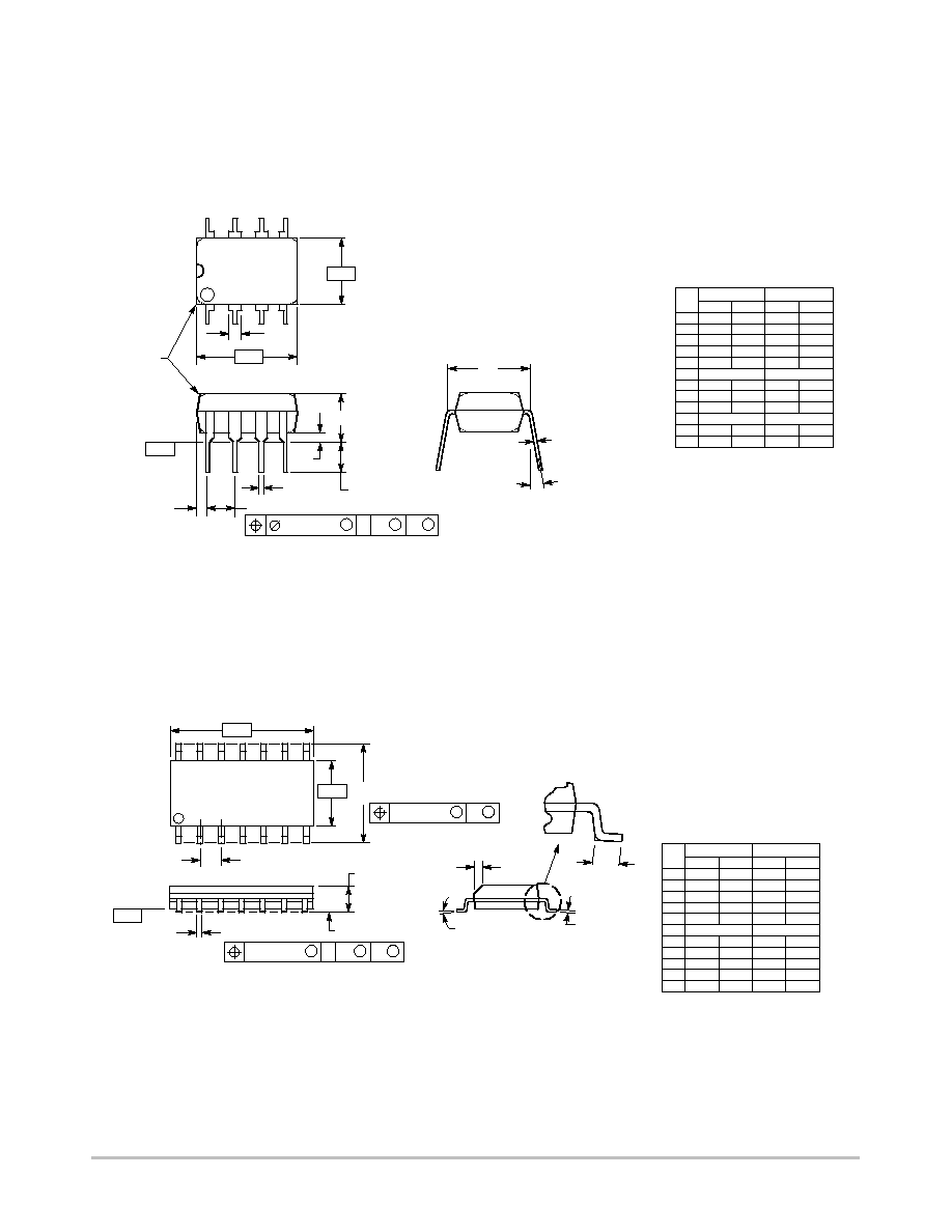
PACKAGE DIMENSIONS
PDIP≠8
N SUFFIX
CASE 626≠05
ISSUE L
NOTES:
1. DIMENSION L TO CENTER OF LEAD WHEN
FORMED PARALLEL.
2. PACKAGE CONTOUR OPTIONAL (ROUND OR
SQUARE CORNERS).
3. DIMENSIONING AND TOLERANCING PER ANSI
Y14.5M, 1982.
1
4
5
8
F
NOTE 2
≠A≠
≠B≠
≠T≠
SEATING
PLANE
H
J
G
D
K
N
C
L
M
M
A
M
0.13 (0.005)
B
M
T
DIM
MIN
MAX
MIN
MAX
INCHES
MILLIMETERS
A
9.40
10.16
0.370
0.400
B
6.10
6.60
0.240
0.260
C
3.94
4.45
0.155
0.175
D
0.38
0.51
0.015
0.020
F
1.02
1.78
0.040
0.070
G
2.54 BSC
0.100 BSC
H
0.76
1.27
0.030
0.050
J
0.20
0.30
0.008
0.012
K
2.92
3.43
0.115
0.135
L
7.62 BSC
0.300 BSC
M
---
10
---
10
N
0.76
1.01
0.030
0.040
_
_
SO≠14
D SUFFIX
CASE 751A≠03
ISSUE F
NOTES:
1. DIMENSIONING AND TOLERANCING PER ANSI
Y14.5M, 1982.
2. CONTROLLING DIMENSION: MILLIMETER.
3. DIMENSIONS A AND B DO NOT INCLUDE
MOLD PROTRUSION.
4. MAXIMUM MOLD PROTRUSION 0.15 (0.006)
PER SIDE.
5. DIMENSION D DOES NOT INCLUDE DAMBAR
PROTRUSION. ALLOWABLE DAMBAR
PROTRUSION SHALL BE 0.127 (0.005) TOTAL
IN EXCESS OF THE D DIMENSION AT
MAXIMUM MATERIAL CONDITION.
≠A≠
≠B≠
G
P
7 PL
14
8
7
1
M
0.25 (0.010)
B
M
S
B
M
0.25 (0.010)
A
S
T
≠T≠
F
R
X 45
SEATING
PLANE
D
14 PL
K
C
J
M
_
DIM
MIN
MAX
MIN
MAX
INCHES
MILLIMETERS
A
8.55
8.75
0.337
0.344
B
3.80
4.00
0.150
0.157
C
1.35
1.75
0.054
0.068
D
0.35
0.49
0.014
0.019
F
0.40
1.25
0.016
0.049
G
1.27 BSC
0.050 BSC
J
0.19
0.25
0.008
0.009
K
0.10
0.25
0.004
0.009
M
0
7
0
7
P
5.80
6.20
0.228
0.244
R
0.25
0.50
0.010
0.019
_
_
_
_
UC3842A, UC3843A, UC2842A, UC2843A
http://onsemi.com
18
PACKAGE DIMENSIONS
SO≠8
D1 SUFFIX
CASE 751≠07
ISSUE W
SEATING
PLANE
1
4
5
8
N
J
X 45
_
K
NOTES:
1. DIMENSIONING AND TOLERANCING PER ANSI
Y14.5M, 1982.
2. CONTROLLING DIMENSION: MILLIMETER.
3. DIMENSION A AND B DO NOT INCLUDE MOLD
PROTRUSION.
4. MAXIMUM MOLD PROTRUSION 0.15 (0.006) PER
SIDE.
5. DIMENSION D DOES NOT INCLUDE DAMBAR
PROTRUSION. ALLOWABLE DAMBAR
PROTRUSION SHALL BE 0.127 (0.005) TOTAL IN
EXCESS OF THE D DIMENSION AT MAXIMUM
MATERIAL CONDITION.
A
B
S
D
H
C
0.10 (0.004)
DIM
A
MIN
MAX
MIN
MAX
INCHES
4.80
5.00
0.189
0.197
MILLIMETERS
B
3.80
4.00
0.150
0.157
C
1.35
1.75
0.053
0.069
D
0.33
0.51
0.013
0.020
G
1.27 BSC
0.050 BSC
H
0.10
0.25
0.004
0.010
J
0.19
0.25
0.007
0.010
K
0.40
1.27
0.016
0.050
M
0
8
0
8
N
0.25
0.50
0.010
0.020
S
5.80
6.20
0.228
0.244
≠X≠
≠Y≠
G
M
Y
M
0.25 (0.010)
≠Z≠
Y
M
0.25 (0.010)
Z
S
X
S
M
_
_
_
_

UC3842A, UC3843A, UC2842A, UC2843A
http://onsemi.com
19
Notes

UC3842A, UC3843A, UC2842A, UC2843A
http://onsemi.com
20
ON Semiconductor and are trademarks of Semiconductor Components Industries, LLC (SCILLC). SCILLC reserves the right to make changes
without further notice to any products herein. SCILLC makes no warranty, representation or guarantee regarding the suitability of its products for any particular
purpose, nor does SCILLC assume any liability arising out of the application or use of any product or circuit, and specifically disclaims any and all liability,
including without limitation special, consequential or incidental damages. "Typical" parameters which may be provided in SCILLC data sheets and/or
specifications can and do vary in different applications and actual performance may vary over time. All operating parameters, including "Typicals" must be
validated for each customer application by customer's technical experts. SCILLC does not convey any license under its patent rights nor the rights of others.
SCILLC products are not designed, intended, or authorized for use as components in systems intended for surgical implant into the body, or other applications
intended to support or sustain life, or for any other application in which the failure of the SCILLC product could create a situation where personal injury or
death may occur. Should Buyer purchase or use SCILLC products for any such unintended or unauthorized application, Buyer shall indemnify and hold
SCILLC and its officers, employees, subsidiaries, affiliates, and distributors harmless against all claims, costs, damages, and expenses, and reasonable
attorney fees arising out of, directly or indirectly, any claim of personal injury or death associated with such unintended or unauthorized use, even if such claim
alleges that SCILLC was negligent regarding the design or manufacture of the part. SCILLC is an Equal Opportunity/Affirmative Action Employer.
PUBLICATION ORDERING INFORMATION
JAPAN: ON Semiconductor, Japan Customer Focus Center
4≠32≠1 Nishi≠Gotanda, Shinagawa≠ku, Tokyo, Japan 141≠0031
Phone: 81≠3≠5740≠2700
Email: r14525@onsemi.com
ON Semiconductor Website: http://onsemi.com
For additional information, please contact your local
Sales Representative.
UC3842A/D
SENSEFET is a trademark of Semiconductor Components Industries, LLC.
Literature Fulfillment:
Literature Distribution Center for ON Semiconductor
P.O. Box 5163, Denver, Colorado 80217 USA
Phone: 303≠675≠2175 or 800≠344≠3860 Toll Free USA/Canada
Fax: 303≠675≠2176 or 800≠344≠3867 Toll Free USA/Canada
Email: ONlit@hibbertco.com
N. American Technical Support: 800≠282≠9855 Toll Free USA/Canada