 | –≠–ª–µ–∫—Ç—Ä–æ–Ω–Ω—ã–π –∫–æ–º–ø–æ–Ω–µ–Ω—Ç: UMC3NT1 | –°–∫–∞—á–∞—Ç—å:  PDF PDF  ZIP ZIP |
©
Semiconductor Components Industries, LLC, 2004
September, 2004 - Rev. 5
1
Publication Order Number:
UMC2NT1/D
UMC2NT1, UMC3NT1,
UMC5NT1
Preferred Devices
Dual Common
Base-Collector Bias
Resistor Transistors
NPN and PNP Silicon Surface Mount
Transistors with Monolithic Bias
Resistor Network
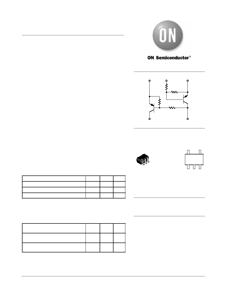
The Bias Resistor Transistor (BRT) contains a single transistor with
a monolithic bias network consisting of two resistors; a series base
resistor and a base-emitter resistor. These digital transistors are
designed to replace a single device and its external resistor bias
network. The BRT eliminates these individual components by
integrating them into a single device. In the UMC2NT1 series, two
complementary BRT devices are housed in the SOT-353 package
which is ideal for low power surface mount applications where board
space is at a premium.
Features
∑
Pb-Free Packages are Available
∑
Simplifies Circuit Design
∑
Reduces Board Space
∑
Reduces Component Count
∑
Available in 8 mm, 7 inch/3000 Unit Tape and Reel
MAXIMUM RATINGS
(T
A
= 25
∞
C unless otherwise noted, common for Q
1
and Q
2
, - minus sign for Q
1
(PNP) omitted)
Rating
Symbol
Value
Unit
Collector-Base Voltage
V
CBO
50
Vdc
Collector-Emitter Voltage
V
CEO
50
Vdc
Collector Current
I
C
100
mAdc
Maximum ratings are those values beyond which device damage can occur.
Maximum ratings applied to the device are individual stress limit values (not
normal operating conditions) and are not valid simultaneously. If these limits
are exceeded, device functional operation is not implied, damage may occur
and reliability may be affected.
THERMAL CHARACTERISTICS
Thermal Resistance - Junction-to-Ambient
(surface mounted)
R
JA
833
∞
C/W
Operating and Storage Temperature Range
T
J
, T
stg
- 65 to
+150
∞
C
Total Package Dissipation
@ T
A
= 25
∞
C (Note 1)
P
D
*
150
mW
1. Device mounted on a FR-4 glass epoxy printed circuit board using the
minimum recommended footprint.
SC-88A/SOT-353
CASE 419A
STYLE 6
Ux = Device Marking
x
= 2, 3 or 5
d
= Date Code
Ux
MARKING
DIAGRAM
1
3
2
5
4
Preferred devices are recommended choices for future use
and best overall value.
4
5
Q1
Q2
R1
R1
R2
R2
3
1
2
d
See detailed ordering and shipping information in the package
dimensions section on page 3 of this data sheet.
ORDERING INFORMATION
http://onsemi.com
UMC2NT1, UMC3NT1, UMC5NT1
http://onsemi.com
2
ELECTRICAL CHARACTERISTICS
(T
A
= 25
∞
C unless otherwise noted)
Characteristic
Symbol
Min
Typ
Max
Unit
Q1 TRANSISTOR: PNP
OFF CHARACTERISTICS
Collector-Base Cutoff Current (V
CB
= 50 V, I
E
= 0)
I
CBO
-
-
100
nAdc
Collector-Emitter Cutoff Current (V
CB
= 50 V, I
B
= 0)
I
CEO
-
-
500
nAdc
Emitter-Base Cutoff Current
UMC2NT1
(V
EB
= 6.0, I
C
= 0 mA)
UMC3NT1
UMC5NT1
I
EBO
-
-
-
-
-
-
0.2
0.5
1.0
mAdc
ON CHARACTERISTICS
Collector-Base Breakdown Voltage (I
C
= 10
µ
A, I
E
= 0)
V
(BR)CBO
50
-
-
Vdc
Collector-Emitter Breakdown Voltage (I
C
= 2.0 mA, I
B
= 0)
V
(BR)CEO
50
-
-
Vdc
DC Current Gain
UMC2NT1
(V
CE
= 10 V, I
C
= 5.0 mA)
UMC3NT1
UMC5NT1
h
FE
60
35
20
100
60
35
-
-
-
Collector-Emitter Saturation Voltage (I
C
= 10 mA, I
B
= 0.3 mA)
V
CE(SAT)
-
-
0.25
Vdc
Output Voltage (on) (V
CC
= 5.0 V, V
B
= 2.5 V, R
L
= 1.0 k
W
)
V
OL
-
-
0.2
Vdc
Output Voltage (off) (V
CC
= 5.0 V, V
B
= 0.5 V, R
L
= 1.0 k
W
)
V
OH
4.9
-
-
Vdc
Input Resistor
UMC2NT1
UMC3NT1
UMC5NT1
R1
15.4
7.0
3.3
22
10
4.7
28.6
13
6.1
k
W
Resistor Ratio
UMC2NT1
UMC3NT1
UMC5NT1
R1/R2
0.8
0.8
0.38
1.0
1.0
0.47
1.2
1.2
0.56
Q2 TRANSISTOR: NPN
OFF CHARACTERISTICS
Collector-Base Cutoff Current (V
CB
= 50 V, I
E
= 0)
I
CBO
-
-
100
nAdc
Collector-Emitter Cutoff Current (V
CB
= 50 V, I
B
= 0)
I
CEO
-
-
500
nAdc
Emitter-Base Cutoff Current
UMC2NT1
(V
EB
= 6.0, I
C
= 0 mA)
UMC3NT1
UMC5NT1
I
EBO
-
-
-
-
-
-
0.2
0.5
0.1
mAdc
ON CHARACTERISTICS
Collector-Base Breakdown Voltage (I
C
= 10
µ
A, I
E
= 0)
V
(BR)CBO
50
-
-
Vdc
Collector-Emitter Breakdown Voltage (I
C
= 2.0 mA, I
B
= 0)
V
(BR)CEO
50
-
-
Vdc
DC Current Gain
UMC2NT1
(V
CE
= 10 V, I
C
= 5.0 mA)
UMC3NT1
UMC5NT1
h
FE
60
35
80
100
60
140
-
-
-
Collector-Emitter Saturation Voltage (I
C
= 10 mA, I
B
= 0.3 mA)
V
CE(SAT)
-
-
0.25
Vdc
Output Voltage (on) (V
CC
= 5.0 V, V
B
= 2.5 V, R
L
= 1.0 k
W
)
V
OL
-
-
0.2
Vdc
Output Voltage (off) (V
CC
= 5.0 V, V
B
= 0.5 V, R
L
= 1.0 k
W
)
V
OH
4.9
-
-
Vdc
Input Resistor
UMC2NT1
UMC3NT1
UMC5NT1
R1
15.4
7.0
33
22
10
47
28.6
13
61
k
W
Resistor Ratio
UMC2NT1
UMC3NT1
UMC5NT1
R1/R2
0.8
0.8
0.8
1.0
1.0
1.0
1.2
1.2
1.2
UMC2NT1, UMC3NT1, UMC5NT1
http://onsemi.com
3
ORDERING INFORMATION
Device
Package
Shipping
UMC2NT1
SC-88A/SOT-353
3000 / Tape & Reel
UMC2NT1G
SC-88A/SOT-353
(Pb-Free)
3000 / Tape & Reel
UMC3NT1
SC-88A/SOT-353
3000 / Tape & Reel
UMC3NT1G
SC-88A/SOT-353
(Pb-Free)
3000 / Tape & Reel
UMC3NT2
SC-88A/SOT-353
3000 / Tape & Reel
UMC5NT1
SC-88A/SOT-353
3000 / Tape & Reel
UMC5NT2
SC-88A/SOT-353
3000 / Tape & Reel
UMC5NT2G
SC-88A/SOT-353
(Pb-Free)
3000 / Tape & Reel
For information on tape and reel specifications, including part orientation and tape sizes, please refer to our Tape and Reel Packaging
Specifications Brochure, BRD8011/D.
DEVICE MARKING AND RESISTOR VALUES
Transistor 1 - PNP
Transistor 2 - NPN
Device
Marking
R1 (K)
R2 (K)
R1 (K)
R2 (K)
UMC2NT1
UMC3NT1
UMC3NT2
UMC5NT1
UMC5NT2
U2
U3
U3
U5
U5
22
10
10
4.7
4.7
22
10
10
10
10
22
10
10
47
47
22
10
10
47
47
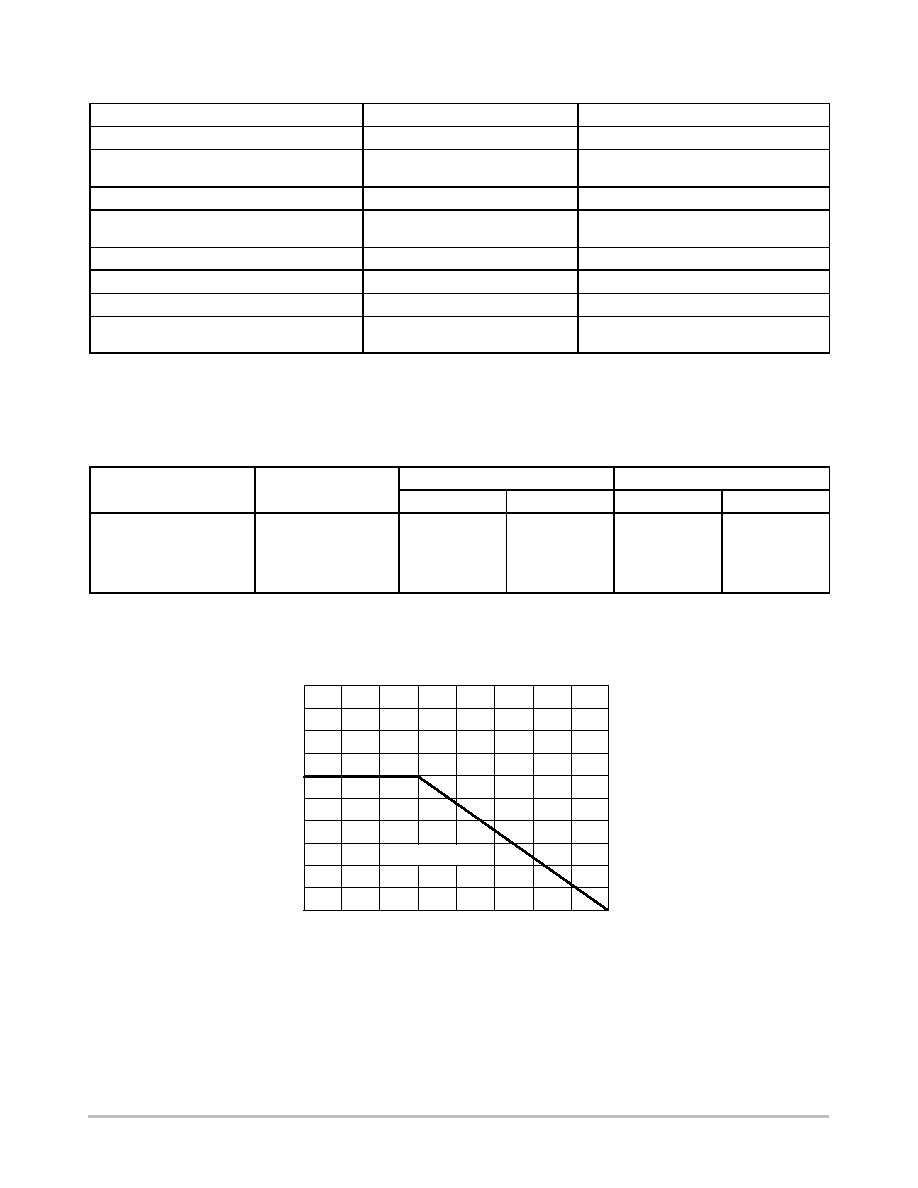
Figure 1. Derating Curve
250
200
150
100
50
0
-50
0
50
100
150
T
A
, AMBIENT TEMPERATURE (
∞
C)
P D
, POWER DISSIP
A
TION (MILLIW
A
TTS)
R
JA
= 833
∞
C/W
UMC2NT1, UMC3NT1, UMC5NT1
http://onsemi.com
4
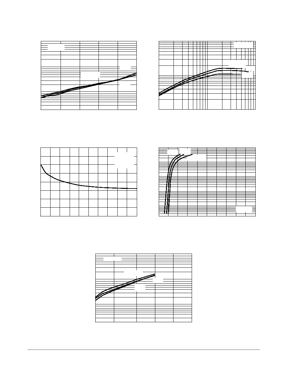
TYPICAL ELECTRICAL CHARACTERISTICS -- UMC2NT1 PNP TRANSISTOR
V in
, INPUT
VOL
T
AGE (VOL
TS)
I C
, COLLECT
OR CURRENT
(mA)
h FE
, DC CURRENT
GAIN
Figure 2. V
CE(sat)
versus I
C
Figure 3. DC Current Gain
1000
10
I
C
, COLLECTOR CURRENT (mA)
100
10
1
100
Figure 4. Output Capacitance
I
C
, COLLECTOR CURRENT (mA)
0
10
20
30
V
O
= 0.2 V
T
A
= -25
∞
C
75
∞
C
100
10
1
0.1
40
50
Figure 5. Output Current versus Input Voltage
100
10
1
0.1
0.01
0.001 0 1
2
3
4
V
in
, INPUT VOLTAGE (VOLTS)
5
6
7
8
9
10
Figure 6. Input Voltage versus Output Current
0.01
V CE(sat)
, MAXIMUM COLLECT
OR VOL
T
AGE (VOL
TS)
0.1
1
10
40
I
C
, COLLECTOR CURRENT (mA)
0
20
50
75
∞
C
25
∞
C
T
A
= -25
∞
C
50
0
10
20
30
40
4
3
2
1
0
V
R
, REVERSE BIAS VOLTAGE (VOLTS)
C ob
, CAP
ACIT
ANCE (pF)
25
∞
C
I
C
/I
B
= 10
25
∞
C
-25
∞
C
V
CE
= 10 V
T
A
= 75
∞
C
f = 1 MHz
l
E
= 0 mA
T
A
= 25
∞
C
75
∞
C
25
∞
C
T
A
= -25
∞
C
V
O
= 5 V
UMC2NT1, UMC3NT1, UMC5NT1
http://onsemi.com
5
TYPICAL ELECTRICAL CHARACTERISTICS -- UMC2NT1 NPN TRANSISTOR
V in
, INPUT
VOL
T
AGE (VOL
TS)
I C
, COLLECT
OR CURRENT
(mA)
h FE
, DC CURRENT
GAIN
Figure 7. V
CE(sat)
versus I
C
10
0
20
30
I
C
, COLLECTOR CURRENT (mA)
10
1
0.1
T
A
= -25
∞
C
75
∞
C
25
∞
C
40
50
Figure 8. DC Current Gain
Figure 9. Output Capacitance
1
0.1
0.01
0.001
0
20
40
50
I
C
, COLLECTOR CURRENT (mA)
V CE(sat)
, MAXIMUM COLLECT
OR VOL
T
AGE (VOL
TS)
1000
100
10
1
10
100
I
C
, COLLECTOR CURRENT (mA)
T
A
= 75
∞
C
25
∞
C
-25
∞
C
T
A
= -25
∞
C
25
∞
C
Figure 10. Output Current versus Input Voltage
75
∞
C
25
∞
C
T
A
= -25
∞
C
100
10
1
0.1
0.01
0.001
0
1
2
3
4
V
in
, INPUT VOLTAGE (VOLTS)
5
6
7
8
9
10
Figure 11. Input Voltage versus Output
Current
50
0
10
20
30
40
4
3
1
2
0
V
R
, REVERSE BIAS VOLTAGE (VOLTS)
C ob
, CAP
ACIT
ANCE (pF)
75
∞
C
V
CE
= 10 V
f = 1 MHz
I
E
= 0 mA
T
A
= 25
∞
C
V
O
= 5 V
V
O
= 0.2 V
I
C
/I
B
= 10
UMC2NT1, UMC3NT1, UMC5NT1
http://onsemi.com
6
TYPICAL ELECTRICAL CHARACTERISTICS -- UMC3NT1 PNP TRANSISTOR
V in
, INPUT
VOL
T
AGE (VOL
TS)
I C
, COLLECT
OR CURRENT
(mA)
h FE
, DC CURRENT
GAIN
Figure 12. V
CE(sat)
versus I
C
100
10
1
0.1
0.01
0.001
0
V
in
, INPUT VOLTAGE (VOLTS)
T
A
= -25
∞
C
25
∞
C
1
2
3
4
5
6
7
8
9
10
Figure 13. DC Current Gain
Figure 14. Output Capacitance
Figure 15. Output Current versus Input
Voltage
Figure 16. Input Voltage versus Output
Current
0.01
20
I
C
, COLLECTOR CURRENT (mA)
V CE(sat)
, MAXIMUM COLLECT
OR VOL
T
AGE (VOL
TS)
0.1
1
0
40
50
1000
1
10
100
I
C
, COLLECTOR CURRENT (mA)
T
A
= 75
∞
C
-25
∞
C
100
10
0
I
C
, COLLECTOR CURRENT (mA)
0.1
1
10
100
10
20
30
40
50
T
A
= -25
∞
C
25
∞
C
75
∞
C
75
∞
C
I
C
/I
B
= 10
50
0
10
20
30
40
4
3
1
2
V
R
, REVERSE BIAS VOLTAGE (VOLTS)
C ob
, CAP
ACIT
ANCE (pF)
0
T
A
= -25
∞
C
25
∞
C
75
∞
C
25
∞
C
V
CE
= 10 V
f = 1 MHz
l
E
= 0 mA
T
A
= 25
∞
C
V
O
= 5 V
V
O
= 0.2 V
UMC2NT1, UMC3NT1, UMC5NT1
http://onsemi.com
7
TYPICAL ELECTRICAL CHARACTERISTICS -- UMC3NT1 NPN TRANSISTOR
V in
, INPUT
VOL
T
AGE (VOL
TS)
I C
, COLLECT
OR CURRENT
(mA)
h FE
, DC CURRENT
GAIN
Figure 17. V
CE(sat)
versus I
C
Figure 18. DC Current Gain
Figure 19. Output Capacitance
Figure 20. Output Current versus Input Voltage
1000
10
I
C
, COLLECTOR CURRENT (mA)
T
A
= 75
∞
C
25
∞
C
-25
∞
C
100
10
1
100
75
∞
C
25
∞
C
100
0
V
in
, INPUT VOLTAGE (VOLTS)
10
1
0.1
0.01
0.001
2
4
6
8
10
T
A
= -25
∞
C
0
I
C
, COLLECTOR CURRENT (mA)
100
T
A
= -25
∞
C
75
∞
C
10
1
0.1
10
20
30
40
50
25
∞
C
Figure 21. Input Voltage versus Output
Current
0.001
V CE(sat)
, MAXIMUM COLLECT
OR VOL
T
AGE (VOL
TS)
T
A
= -25
∞
C
75
∞
C
25
∞
C
0.01
0.1
1
40
I
C
, COLLECTOR CURRENT (mA)
0
20
50
50
0
10
20
30
40
4
3
2
1
0
V
R
, REVERSE BIAS VOLTAGE (VOLTS)
C ob
, CAP
ACIT
ANCE (pF)
I
C
/I
B
= 10
V
CE
= 10 V
f = 1 MHz
I
E
= 0 mA
T
A
= 25
∞
C
V
O
= 5 V
V
O
= 0.2 V

UMC2NT1, UMC3NT1, UMC5NT1
http://onsemi.com
8
TYPICAL ELECTRICAL CHARACTERISTICS -- UMC5NT1 PNP TRANSISTOR
25
∞
C
I C
, COLLECT
OR CURRENT
(mA)
h FE
, DC CURRENT
GAIN
Figure 22. V
CE(sat)
versus I
C
Figure 23. DC Current Gain
Figure 24. Output Capacitance
Figure 25. Output Current versus Input Voltage
1000
10
I
C
, COLLECTOR CURRENT (mA)
T
A
= 75
∞
C
25
∞
C
-25
∞
C
100
1
1
1000
75
∞
C
25
∞
C
100
0
V
in
, INPUT VOLTAGE (VOLTS)
10
1
0.1
0.01
2
4
6
8
12
T
A
= -25
∞
C
V CE(sat)
, MAXIMUM COLLECT
OR VOL
T
AGE (VOL
TS)
T
A
= 75
∞
C
-25
∞
C
0.01
0.1
1
40
I
C
, COLLECTOR CURRENT (mA)
0
20
50
0
10
20
30
40
12
6
4
2
0
V
R
, REVERSE BIAS VOLTAGE (VOLTS)
C ob
, CAP
ACIT
ANCE (pF)
I
C
/I
B
= 10
V
CE
= 10 V
f = 1 MHz
I
E
= 0 mA
T
A
= 25
∞
C
V
O
= 5 V
30
10
60
100
10
10
8
15
25
35
45
5
SERIES 1
10

UMC2NT1, UMC3NT1, UMC5NT1
http://onsemi.com
9
TYPICAL ELECTRICAL CHARACTERISTICS -- UMC5NT1 NPN TRANSISTOR
V in
, INPUT
VOL
T
AGE (VOL
TS)
I C
, COLLECT
OR CURRENT
(mA)
h FE
, DC CURRENT
GAIN
Figure 26. V
CE(sat)
versus I
C
0
2
4
6
8
10
100
10
1
0.1
0.01
0.001
V
in
, INPUT VOLTAGE (VOLTS)
T
A
= -25
∞
C
75
∞
C
25
∞
C
Figure 27. DC Current Gain
Figure 28. Output Capacitance
100
10
1
0.1
0
10
20
30
40
50
I
C
, COLLECTOR CURRENT (mA)
Figure 29. Output Current versus Input Voltage
1000
10
I
C
, COLLECTOR CURRENT (mA)
T
A
= 75
∞
C
25
∞
C
-25
∞
C
100
10 1
100
25
∞
C
75
∞
C
50
0
10
20
30
40
1
0.8
0.6
0.4
0.2
0
V
R
, REVERSE BIAS VOLTAGE (VOLTS)
C ob
, CAP
ACIT
ANCE (pF)
Figure 30. Input Voltage versus Output Current
0
20
40
50
10
1
0.1
0.01
I
C
, COLLECTOR CURRENT (mA)
25
∞
C
75
∞
C
V CE(sat)
, MAXIMUM COLLECT
OR VOL
T
AGE (VOL
TS)
V
CE
= 10 V
f = 1 MHz
I
E
= 0 mA
T
A
= 25
∞
C
V
O
= 5 V
V
O
= 0.2 V
I
C
/I
B
= 10
T
A
= -25
∞
C
T
A
= -25
∞
C

UMC2NT1, UMC3NT1, UMC5NT1
http://onsemi.com
10
PACKAGE DIMENSIONS
SC-88A/SOT-353
CASE 419A-02
ISSUE G
STYLE 6:
PIN 1. EMITTER 2
2. BASE 2
3. EMITTER 1
4. COLLECTOR 1
5. BASE 1/COLLECTOR 2
B
0.2 (0.008)
M
M
1
2
3
4
5
A
G
S
D
5 PL
H
C
N
J
K
-B-
NOTES:
1. DIMENSIONING AND TOLERANCING
PER ANSI Y14.5M, 1982.
2. CONTROLLING DIMENSION: INCH.
3. 419A-01 OBSOLETE. NEW STANDARD
419A-02.
4. DIMENSIONS A AND B DO NOT INCLUDE
MOLD FLASH, PROTRUSIONS, OR GATE
BURRS.
DIM
A
MIN
MAX
MIN
MAX
MILLIMETERS
1.80
2.20
0.071
0.087
INCHES
B
1.15
1.35
0.045
0.053
C
0.80
1.10
0.031
0.043
D
0.10
0.30
0.004
0.012
G
0.65 BSC
0.026 BSC
H
---
0.10
---
0.004
J
0.10
0.25
0.004
0.010
K
0.10
0.30
0.004
0.012
N
0.20 REF
0.008 REF
S
2.00
2.20
0.079
0.087
mm
inches
SCALE 20:1
0.65
0.025
0.65
0.025
0.50
0.0197
0.40
0.0157
1.9
0.0748
*For additional information on our Pb-Free strategy and soldering
details, please download the ON Semiconductor Soldering and
Mounting Techniques Reference Manual, SOLDERRM/D.
SOLDERING FOOTPRINT*
ON Semiconductor and are registered trademarks of Semiconductor Components Industries, LLC (SCILLC). SCILLC reserves the right to make changes without further notice
to any products herein. SCILLC makes no warranty, representation or guarantee regarding the suitability of its products for any particular purpose, nor does SCILLC assume any liability
arising out of the application or use of any product or circuit, and specifically disclaims any and all liability, including without limitation special, consequential or incidental damages.
"Typical" parameters which may be provided in SCILLC data sheets and/or specifications can and do vary in different applications and actual performance may vary over time. All
operating parameters, including "Typicals" must be validated for each customer application by customer's technical experts. SCILLC does not convey any license under its patent rights
nor the rights of others. SCILLC products are not designed, intended, or authorized for use as components in systems intended for surgical implant into the body, or other applications
intended to support or sustain life, or for any other application in which the failure of the SCILLC product could create a situation where personal injury or death may occur. Should
Buyer purchase or use SCILLC products for any such unintended or unauthorized application, Buyer shall indemnify and hold SCILLC and its officers, employees, subsidiaries, affiliates,
and distributors harmless against all claims, costs, damages, and expenses, and reasonable attorney fees arising out of, directly or indirectly, any claim of personal injury or death
associated with such unintended or unauthorized use, even if such claim alleges that SCILLC was negligent regarding the design or manufacture of the part. SCILLC is an Equal
Opportunity/Affirmative Action Employer. This literature is subject to all applicable copyright laws and is not for resale in any manner.
PUBLICATION ORDERING INFORMATION
N. American Technical Support: 800-282-9855 Toll Free
USA/Canada
Japan: ON Semiconductor, Japan Customer Focus Center
2-9-1 Kamimeguro, Meguro-ku, Tokyo, Japan 153-0051
Phone: 81-3-5773-3850
UMC2NT1/D
LITERATURE FULFILLMENT:
Literature Distribution Center for ON Semiconductor
P.O. Box 61312, Phoenix, Arizona 85082-1312 USA
Phone: 480-829-7710 or 800-344-3860 Toll Free USA/Canada
Fax: 480-829-7709 or 800-344-3867 Toll Free USA/Canada
Email: orderlit@onsemi.com
ON Semiconductor Website: http://onsemi.com
Order Literature: http://www.onsemi.com/litorder
For additional information, please contact your
local Sales Representative.