
Fea tures
∑
Surface mountable on ceramic or
printed circuit board
∑
Miniature package saves circuit board
area
∑
Electrical performance similar to
4N22A and 4N24A
∑
Hermetically sealed
∑
Screened per MIL-PRF-19500 TX and
TXV equivalent levels or per ESA
5000
(6)
De scrip tion
The HCC240 and HCC242 are optically
coupled isolators, consisting of a gallium
aluminum arsenide LED and a silicon
phototransistor mounted and coupled in
a miniature surface mount hermetic
leadless chip carrier. The HCC240 and
HCC242 are identical except for the DC
current transfer ratio. Electrical
parameters are similar to the JEDEC
registered 4N22A and 4N24A. These
solid state couplers are ideal for designs
where board space and device weight
are important design considerations.
Typical screening and lot acceptance
tests are provided on page 13-4. The
burn-in condition is V
CE
= 9 V, P
D
= 275
mW, I
F
= 20-50 mA (adjusted to achieve
PD). No HTRB is performed on this
device.
Ab so lute Maxi mum Rat ings (T
A
= 25
o
C un less oth er wise noted)
Input- to- Output Iso la tion Volt age . . . . . . . . . . . . . . . . . . . . . . . . . . . . . . . ±1.0 kVDC
(1)
Op er at ing Tem pera ture . . . . . . . . . . . . . . . . . . . . . . . . . . . . . . . . . . -55
o
C to +125
o
C
Stor age Tem pera ture . . . . . . . . . . . . . . . . . . . . . . . . . . . . . . . . . . . . -65
o
C to +150
o
C
Sol der ing Tem pera ture (va por phase re flow for 30 sec.) . . . . . . . . . . . . . . . . . 215
o
C
Sol der ing Tem pera ture (heated collet for 5 sec.) . . . . . . . . . . . . . . . . . . . . . . . 260
o
C
In put Di ode
For ward DC Cur rent (65
o
C be low) . . . . . . . . . . . . . . . . . . . . . . . . . . . . . . . . . . 40 mA
Re verse Volt age. . . . . . . . . . . . . . . . . . . . . . . . . . . . . . . . . . . . . . . . . . . . . . . . . . 2.0 V
Power Dis si pa tion . . . . . . . . . . . . . . . . . . . . . . . . . . . . . . . . . . . . . . . . . . . . . 60 mW
(2)
Out put Pho to tran sis tor
Con tinu ous Col lec tor Cur rent . . . . . . . . . . . . . . . . . . . . . . . . . . . . . . . . . . . . . . . 50 mA
Collector- Emitter Volt age . . . . . . . . . . . . . . . . . . . . . . . . . . . . . . . . . . . . . . . . . . 30 V
(3)
Emitter- Collector Volt age . . . . . . . . . . . . . . . . . . . . . . . . . . . . . . . . . . . . . . . . . 5.0 V
(4)
Power Dis si pa tion . . . . . . . . . . . . . . . . . . . . . . . . . . . . . . . . . . . . . . . . . . . . 300 mW
(5)
Notes:
(1) Measured with inputs shorted together and outputs shorted together.
(2) Derate linearly 1.0 mW/
o
C above 65
o
C.
(3) HCC240HV and HCC242HV are available rated at 55 V minimum.
(4) HCC240HV and HCC242HV are available rated at 7.0 V minimim.
(5) Derate linearly 3.0 mW/
o
C above 25
o
C.
(6) Some deviations from ESA 5000 apply. See page 13-4 for details.
Prod uct Bul le tin HCC240
Sep tem ber 1996
Sur face Mount Op ti cally Cou pled Iso la tor
Types HCC240, HCC242, TX, TXV, ESA- XN
Op tek Tech nol ogy, Inc. 1215 W. Crosby Road Car roll ton, Texas 75006 (972) 323- 2200 Fax (972) 323- 2396
15-28
Types HCC240, HCC242, TX, TXV, ESA-XN
Optek reserves the right to make changes at any time in order to improve design and to supply the best product possible.
Op tek Tech nol ogy, Inc. 1215 W. Crosby Road Car roll ton, Texas 75006 (972) 323- 2200 Fax (972) 323- 2396
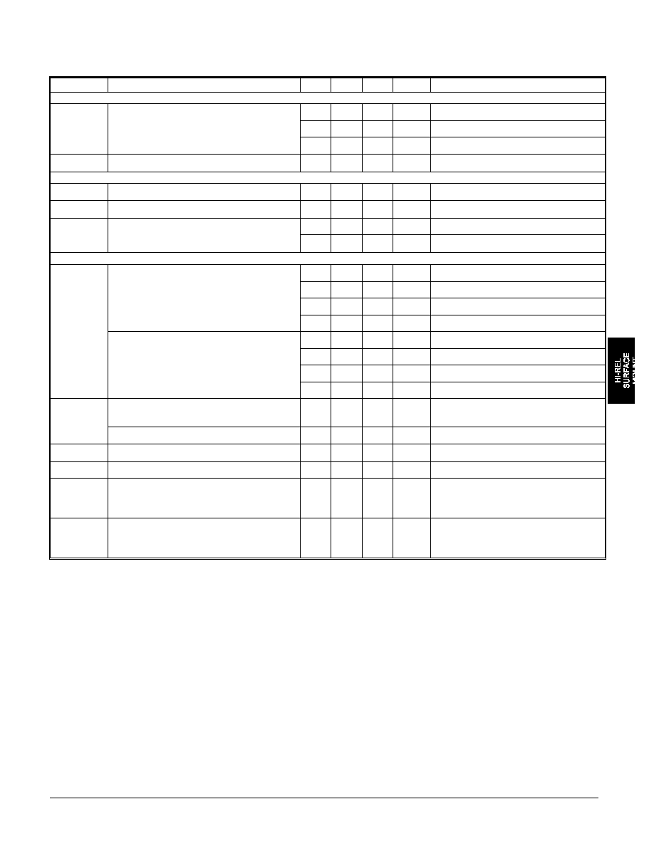
Elec tri cal Char ac ter is tics (T
A
= 25
o
C un less oth er wise noted)
SYM BOL
PA RAME TER
MIN TYP MAX UNITS
TEST CON DI TIONS
In put Di ode
V
F
Forward Voltage
0.80
1.5
V
I
F
= 10.0 mA
1.00
1.7
V
I
F
= 10.0 mA, T
A
= -55
o
C
0.70
1.3
V
I
F
= 10.0 mA, T
A
= 100
o
C
I
R
Reverse Current
100
µ
A
V
R
= 2.0 V
Out put Pho to tran sis tor
V
(BR)CEO
Collector-Emitter Breakdown Voltage
(3)
30
V
I
C
= 1.0 mA, I
F
= 0
V
(BR)ECO
Emitter-Collector Breakdown Voltage
(4)
5.0
V
I
E
= 100
µ
A, I
F
= 0
I
C(OFF)
Collector-Emitter Dark Current
100
nA
V
CE
= 20 V, I
F
= 0
100
µ
A
V
CE
= 20 V, I
F
= 0, T
A
= 100
o
C
Cou pled
I
C(ON)
On-State Collector Current
HCC240
0.15
mA
V
CE
= 5.0 V, I
F
= 2.0 mA
2.5
6.0
mA
V
CE
= 5.0 V, I
F
= 10.0 mA
1.0
mA
V
CE
= 5.0 V, I
F
= 10.0 mA, T
A
= -55
o
C
1.0
mA
V
CE
= 5.0 V, I
F
= 10.0 mA, T
A
= 100
o
C
HCC242
0.40
mA
V
CE
= 5.0 V, I
F
= 2.0 mA
10.0
15.0
mA
V
CE
= 5.0 V, I
F
= 10.0 mA
4.0
mA
V
CE
= 5.0 V, I
F
= 10.0 mA, T
A
= -55
o
C
4.0
mA
V
CE
= 5.0 V, I
F
= 10.0 mA, T
A
= 100
o
C
V
CE(SAT)
Collector-Emitter Saturation Voltage
HCC240
0.30
V
I
C
= 2.5 mA, I
F
= 20.0 mA
HCC242
0.30
V
I
C
= 10.0 mA, I
F
= 20.0 mA
R
I-O
Resistance (Input to Output)
10
11
V
I-O
= ±1000 VDC
(1)
C
I-O
Capacitance (Input to Output)
5.0
pF
V
I-O
= 0.0 V, f = 1.0 MHz
(1)
t
r
Output Rise Time
HCC240
HCC242
15.0
20.0
µ
s
µ
s
V
CC
= 10.0 V, I
F
= 10.0 mA, R
L
= 100
t
f
Output Fall Time
HCC240
HCC242
15.0
20.0
µ
s
µ
s
V
CC
= 10.0 V, I
F
= 10.0 mA, R
L
= 100
15-29