Fea tures
∑
Narrow receiving angle
∑
Fast switching time
∑
Linear response vs. irradiance
∑
Enhanced temperature range
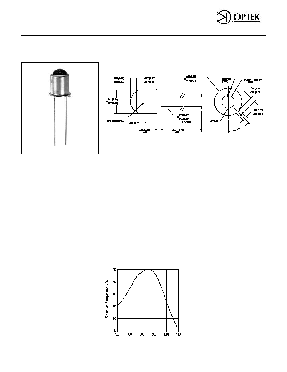
De scrip tion
The OP910 consists of a PIN silicon
photodiode mounted in a two-leaded
hermetic TO-46 package. The narrow
receiving angle has an acceptance half
angle of
±
12
o
.
Ab so lute Maxi mum Rat ings (T
A
= 25
o
C un less oth er wise noted)
Re verse Volt age . . . . . . . . . . . . . . . . . . . . . . . . . . . . . . . . . . . . . . . . . . . . . . . . . . 60 V
Stor age Tem per ature Range . . . . . . . . . . . . . . . . . . . . . . . . . . . . . . -65
o
C to +150
o
C
Op er at ing Tem per ature Range . . . . . . . . . . . . . . . . . . . . . . . . . . . . -65
o
C to +125
o
C
Lead Sol der ing Tem per ature [1/16 inch (1.6 mm) from case for 5 sec . with sol der ing
iron] . . . . . . . . . . . . . . . . . . . . . . . . . . . . . . . . . . . . . . . . . . . . . . . . . . . . . . . . 260
o
C
(1)
Power Dissaipa tion . . . . . . . . . . . . . . . . . . . . . . . . . . . . . . . . . . . . . . . . . . . . . 250 mW
NOTES:
(1) RMA Flux is rec om mended. Du ra tion can be ex tended to 10 sec. max. when flow
sol der ing.
(2) Light source is an un fil tered GaAIAs LED with a peak wave length of 885 nm and a radio met
ric in ten sity level which var ies less than 10% over the en tire lens sur face of the
pho to di ode being tested.
(3) Junc tion tem pera ture main tained at 25
o
C.
(4) To cal cu late typi cal dark cur rent in nA, use. The for mual I
D
= 10
(0.042 T
A
t-1.5)
where T
A
is
am bi ent tem pera ture in
o
C.
(5) Der ate line arly 2.5 mw/
o
C above 25
o
C.
Prod uct Bul le tin OP910
December 1998
PIN Sili con Photodiode
Type OP910
Optek Tech nol ogy, Inc. 1215 W. Crosby Road Car roll ton, Texas 75006 (972)323- 2200 Fax (972)323-2396
3-70
*THIS DIMENSION
CONTROLLED AT HOUSING SURFACE.
DIMENSIONS ARE IN INCHES (MILLIMETERS).
Wave length - nm
Typi cal Spec tral Re sponse
Typi cal Per form ance Curves
Type OP910
Op tek re serves the right to make changes at any time in or der to im prove de sign and to sup ply the best prod uct pos si ble.
Op tek Tech nol ogy, Inc. 1215 W. Crosby Road Car roll ton, Texas 75006 (972)323- 2200 Fax (972)323-2396
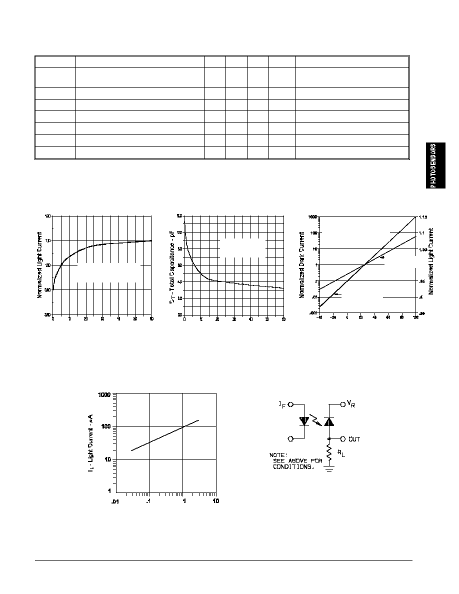
Elec tri cal Char ac ter is tics (T
A
= 25
o
C un less oth er wise noted)
SYM BOL
PA RAME TER
MIN TYP MAX UNITS
TEST CON DI TIONS
I
L
Light Current
10
13
µ
A
V
R
= 20 V, E
e
= .50 mW/cm
2
note
2,3
I
D
Dark Current
1
10
nA
V
R
= 20 V, E
e
= 0.0
V
(BR)R
Reverse Voltage Breakdown
100
V
I
R
= 100
µ
A
t
r
Rise Time
10
nS
V
R
= 20 V, R
L
= 50 OHMS
t
f
Fall Time
10
nS
V
R
= 20 V, R
L
= 50 OHMS
Half Angle
+/- 12
degr. I
F
= Constant
C
P
Capacitance
13
pF
V
R
= 0 V, F = 1 Mhz, E
e
= 0
Typi cal Per form ance Curves
Normalized Light Current vs
Reverse Voltage
V
R
- Reverse Voltage - V
T
A
= 25
o
C
= 935 nm
Total Capacitance vs
Reverse Voltage
V
R
- Reverse Voltage - V
T
A
= 25
o
C
E
e
= 0 mW/cm
2
f = 1 MHz
Normalized Light and Dark
Current vs Ambient Temperature
T
A
- Ambient Temperature -
o
C
V
R
= 5 V
= 935 nm
Normalized to T
A
= 25
o
C
Dark Current
Light Current
Light Current vs Irradiance
Switching Time Test Circuit
3-71
E
e
- Irradiance - mW/cm
2