 | –≠–ª–µ–∫—Ç—Ä–æ–Ω–Ω—ã–π –∫–æ–º–ø–æ–Ω–µ–Ω—Ç: OPB696B | –°–∫–∞—á–∞—Ç—å:  PDF PDF  ZIP ZIP |
Fea tures
∑
Photologic
Æ
output
∑
Four output options
∑
Mechanical switch replacement
∑
3-pin connector (Ho Tien L2561-03),
Molex compatible connector 5102
series housing and 5103 series
terminal
De scrip tion
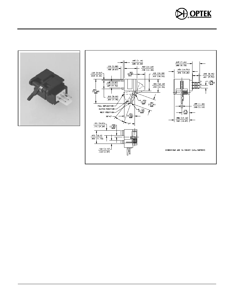
The OPB695 series flag switches consist
of an infrared emitting diode and a
monolithic integrated circuit, which
incorporates a photodiode, a linear
amplifier, and a Schmitt trigger. A lever
arm actuated flag interrupts the light
beam switching the output between
states that can readily drive logic gates.
This switch is designed to easily snap
mount into a 0.037" ± 0.001" (0.94 mm)
thick material with a rectangular opening
of 0.320" ± 0.003" x 0.472" (8.13 mm x
11.99 mm) minimum. Insertion into the
punched side of metal is recommended.
Customized lever arms and spring
torques can be designed for specific
applications.
The device features TTL/LSTTL
compatible logic level output which can
drive up to 10 TTL loads over a voltage
range from 4.5 V to 16 V.
Ab so lute Maxi mum Rat ings (T
A
= 25
o
C un less oth er wise noted)
Stor age Tem pera ture Range . . . . . . . . . . . . . . . . . . . . . . . . . . . . . . -40
o
C to +100
o
C
Op er at ing Tem pera ture Range . . . . . . . . . . . . . . . . . . . . . . . . . . . . -40
o
C to +100
o
C
In put Di ode
For ward DC Cur rent . . . . . . . . . . . . . . . . . . . . . . . . . . . . . . . . . . . . . . . . . . . . . . 50 mA
Peak For ward Cur rent (1
µ
s pulse width, 300 pps) . . . . . . . . . . . . . . . . . . . . . . . . 3.0 A
Re verse DC Volt age. . . . . . . . . . . . . . . . . . . . . . . . . . . . . . . . . . . . . . . . . . . . . . . 3.0 V
Power Dis si pa tion . . . . . . . . . . . . . . . . . . . . . . . . . . . . . . . . . . . . . . . . . . . . 100 mW
(1)
Out put Pho tologic
Æ
Sup ply Volt age, V
CC
. . . . . . . . . . . . . . . . . . . . . . . . . . . . . . . . . . . . . . . . . . . . . . . 18 V
Du ra tion of Out put Short To V
CC
. . . . . . . . . . . . . . . . . . . . . . . . . . . . . . . . . . . 1.00 sec
Volt age at Out put. . . . . . . . . . . . . . . . . . . . . . . . . . . . . . . . . . . . . . . . . . . . . . . . . . 30 V
Low Level Out put Cur rent (sink ing) . . . . . . . . . . . . . . . . . . . . . . . . . . . . . . . . . . 16 mA
Power Dis si pa tion . . . . . . . . . . . . . . . . . . . . . . . . . . . . . . . . . . . . . . . . . . . . 240 mW
(2)
Notes:
(1) Der ate line arly 1.33 mW/
o
C above 25
o
C.
(2) Der ate line arly 2.50 mW/
o
C above 30
o
C.
Prod uct Bul le tin OPB695
July 1996
Photologic
Æ
Optical Flag Switch
Types OPB695, OPB696, OPB697, OPB698 Se ries
Op tek Tech nol ogy, Inc. 1215 W. Crosby Road Car roll ton, Texas 75006 (972)323- 2200 Fax (972)323- 2396
PINOUT
Pin 1: VCC
Pin 2: Output
Pin 3: GND
12-62
Types OPB695, OPB696, OPB697, OPB698 Series
Elec tri cal Char ac ter is tics (T
A
= 25
o
C un less oth er wise noted)
SYM BOL
PA RAME TER
MIN
TYP MAX UNITS
TEST CON DI TIONS
In put Di ode
V
F
Forward Voltage
1.6
V
I
F
= 10 mA
I
R
Reverse Current
100
µ
A
V
R
= 3.0 V
Out put Pho tologic
Æ
Sen sor
V
CC
Operating D.C. Supply Voltage
4.5
5.0
8.0
V
OPB695A, 696A, 697A, 698A
OPB695B, 696B, 697B, 698B
8.0
12.0
13.5
V
OPB695C, 696C, 697C, 698C
13.5
15.0
16.0
V
I
CC
Operating Supply Current
20.0
30.0
mA
V
OH
High Level Output Voltage:
V
CC
-1.5
V
I
OH
= 100
µ
A, Unblocked
Buffer, 10K Pull-up
OPB695A/B/C
Inverter, 10K Pull-up
OPB697A/B/C V
CC
-1.5
V
I
OH
= 100
µ
A, Blocked
(4)
I
OH
High Level Output Current:
100
µ
A
V
CC
= 4.5 to 8 V, V
OH
= 30 V,
Unblocked
Buffer, Open-Collector
OPB696A
OPB696B
100
µ
A
V
CC
= 8 to 13.5 V, V
OH
= 30 V,
Unblocked
OPB696C
100
µ
A
V
CC
= 13.5 to 16 V, V
OH
= 30 V,
Unblocked
Inverter, Open-Collector
OPB698A
100
µ
A
V
CC
= 4.5 to 8 V, V
OH
= 30 V,
Blocked
(4)
OPB698B
100
µ
A
V
CC
= 8 to 13.5 V, V
OH
= 30 V,
Blocked
(4)
OPB698C
100
µ
A
V
CC
= 13.5 to 16 V, V
OH
= 30 V,
Blocked
(4)
V
OL
Low Level Output Voltage:
0.4
V
V
CC
= 4.5 to 8 V, I
OL
= 16 mA,
Blocked
(4)
V
CC
= 8 to 13.5 V, I
OL
= 16 mA,
Blocked
(4)
V
CC
= 13.5 to 16 V, I
OL
= 16 mA,
Blocked
(4)
Buffer, 10K Pull-up
OPB695A/B/C
Buffer, Open-Collector OPB696A/B/C
Inverter, 10K Pull-up
OPB697A/B/C
0.4
V
V
CC
= 4.5 to 8 V, I
OL
= 16 mA,
Unblocked
V
CC
= 8 to 13.5 V, I
OL
= 16 mA,
Unblocked
V
CC
= 13.5 to 16 V, I
OL
= 16 mA,
Unblocked
Inverter, Open-Collector OPB698A/B/C
(4) Test requires lever arm in "blocked" position.
Optek reserves the right to make changes at any time in order to improve design and to supply the best product possible.
Op tek Tech nol ogy, Inc. 1215 W. Crosby Road Car roll ton, Texas 75006 (972)323- 2200 Fax (972)323- 2396
12-63
Types OPB695, OPB696, OPB697, OPB698 Series
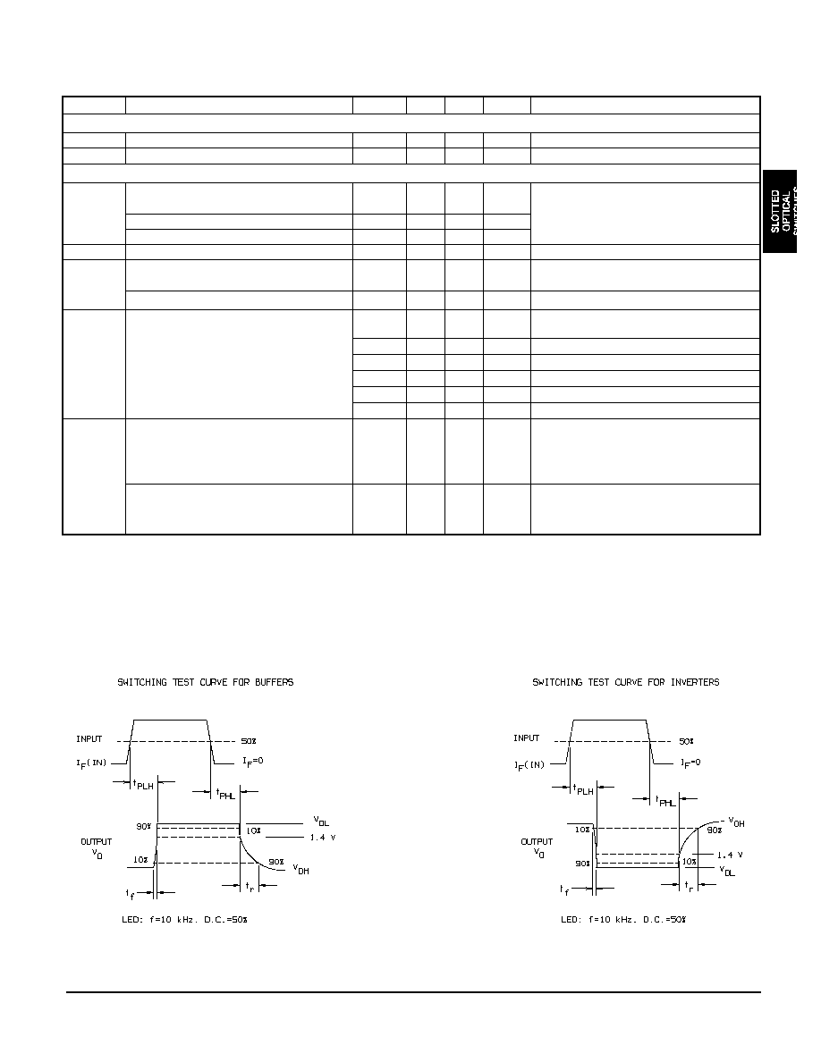
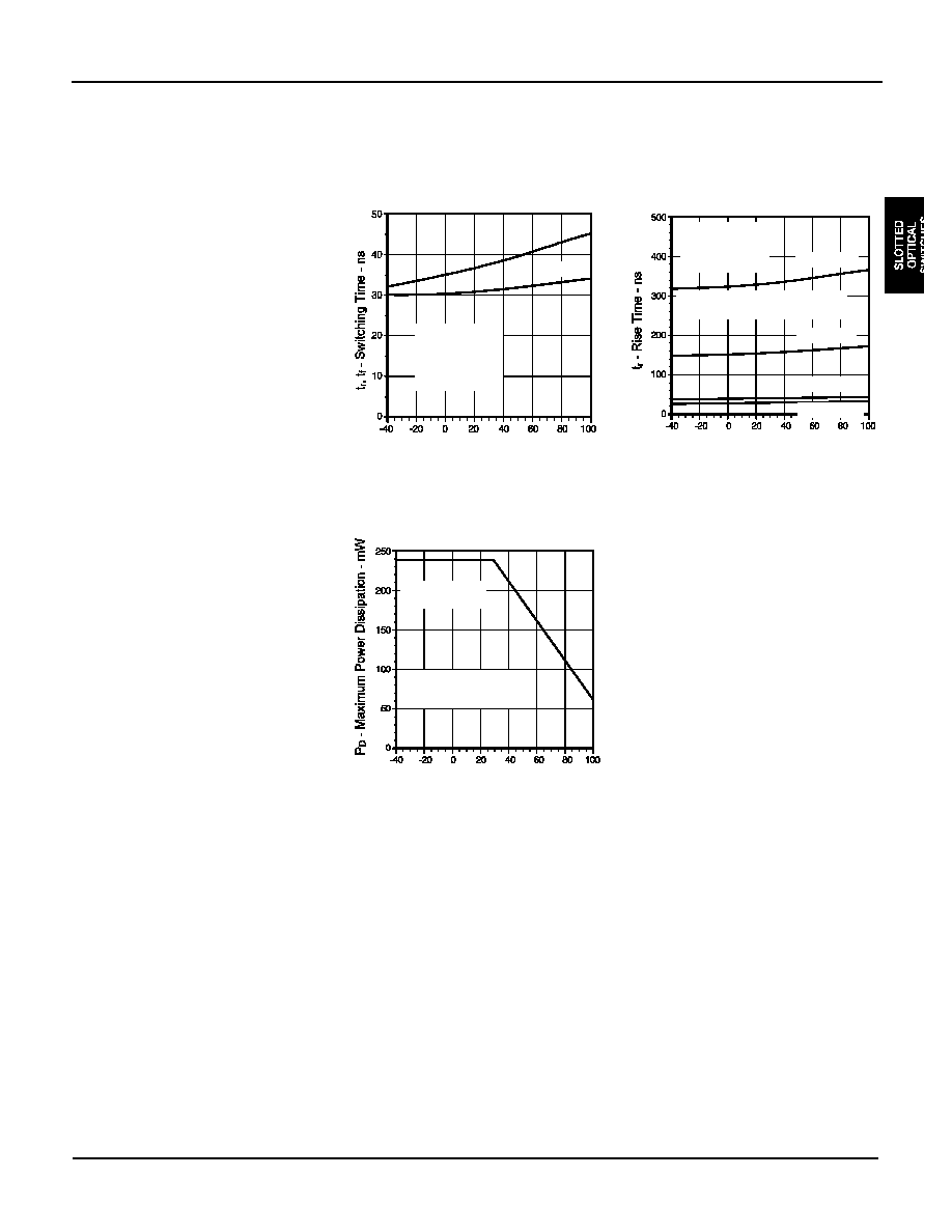
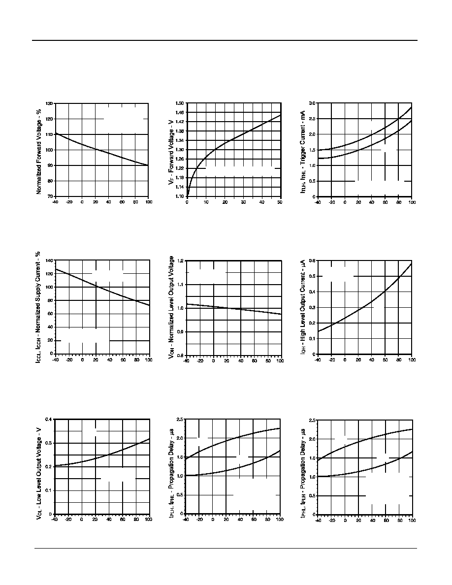
Typi cal Per form ance Curves
Switching Time vs Ambient
Temperature
T
A
- Ambient Temperature -
o
C
Rise Time vs Output Load vs
Ambient Temperature
T
A
- Ambient Temperature -
o
C
Typical Thermal Derating Curve
T
A
- Ambient Temperature -
o
C
Safe Operating
Area
V
CC
= 5 V
I
F
= 0 or 10 mA
f = 10 KHz
DC = 50%
R
L
= 300
t
f
t
r
V
CC
= 5 V
I
F
= 0 or 10 mA
f = 10 KHz
DC = 50%
* - Equivalent Output Load
Including Pull-up if Applicable
R
L
= 2 k
*
R
L
= 390
*
R
L
= 300
*
R
L
= 1 k
*
No Heat Sink;
Derate 2.50 mW/
o
C
Above 30
o
C
Optek reserves the right to make changes at any time in order to improve design and to supply the best product possible.
Op tek Tech nol ogy, Inc. 1215 W. Crosby Road Car roll ton, Texas 75006 (972)323- 2200 Fax (972)323- 2396
12-65
Types OPB695, OPB696, OPB697, OPB698 Series
Typi cal Per form ance Curves
T
A
- Ambient Temperature -
o
C
Normalized Forward Voltage vs
Ambient Temperature
Forward Current vs Forward
Voltage Input Diode
I
F
- Forward Current - mA
Trigger Current vs Ambient
Temperature
T
A
- Ambient Temperature -
o
C
V
CE
= 5 V
I
F
= 5 mA
Normalized to
T
A
= 25
o
C
T
A
- Ambient Temperature -
o
C
Normalized Supply Current vs
Ambient Temperature
OPB695, OPB697 Normalized
High Level Output Voltage vs
Ambient Temperature
T
A
- Ambient Temperature -
o
C
OPB696, OPB698 High Level
Output Current vs Ambient
T
A
- Ambient Temperature -
o
C
Low Level Output Voltage vs
Ambient Temperature
T
A
- Ambient Temperature -
o
C
OPB695, OPB696 Propagation
Delay vs Ambient Temperature
T
A
- Ambient Temperature -
o
C
I
CCH
, I
CCL
V
CC
= 16 V
V
OH
= 30 V
V
CC
= 5 V
I
F
= 0 or 10 mA
f = 10 KHz
DC = 50%
R
L
= 300
I
TLH
I
THL
V
CC
= 5 V
Output Unloaded
V
CC
= 5 V
Output Unloaded
V
CC
= 4.5 V
I
OL
= 16 mA
V
OL
V
OH
V
CC
= 16 V
I
OH
= 100
µ
A
OPB697, OPB698 Propagation
Delay vs Ambient Temperature
T
A
- Ambient Temperature -
o
C
V
CC
= 5 V
I
F
= 0 or 10 mA
f = 10 KHz
DC = 50%
R
L
= 300
t
PLH
t
PHL
I
F
@ 500 ms pulse width
I
OH
t
PHL
t
PLH
Op tek Tech nol ogy, Inc. 1215 W. Crosby Road Car roll ton, Texas 75006 (972)323- 2200 Fax (972)323- 2396
12-64

PART NUM BER GUIDE
OPB 6 9 X X
Op er at ing D.C. Sup ply Volt age:
A - 4.5V
V
CC
8.0V
B - 8.0V
V
CC
13.5V
C - 13.5V
V
CC
16.0V
Elec tri cal Speci fi ca tion Varia tions:
5 - Buffer, 10K Pull- up
6 - Buffer, Open- Collector
7 - Inverter, 10K Pull- up
8 - Inverter, Open- Collector
Sche mat ics
Types OPB695, OPB696, OPB697, OPB698 Series
V
CC
OUT
GND
V
CC
OUT
GND
V
CC
OUT
GND
OPB695...Buffer/10K PU
OPB697...Inverter/10K PU
OPB696...Buffer/OC
V
CC
OUT
GND
OPB698...Inverter/OC
Op tek Tech nol ogy, Inc. 1215 W. Crosby Road Car roll ton, Texas 75006 (972)323- 2200 Fax (972)323- 2396
12- 66