F-51477GNB-FW-AD (AD) No. 2003-0090
OPTREX CORPORATION
Page 1/19
LCD Module Technical Specification
F-51477GNB-FW-AD
Table of Contents
1. General Specifications
.................................................................................................................................. 2
2. Electrical Specifications
............................................................................................................................... 3
3. Optical Specifications
................................................................................................................................... 8
4. I/O Terminal
.................................................................................................................................................... 10
5. Test
................................................................................................................................................................... 12
6. Appearance Standards
............................................................................................................................... 13
7. Code System of Production Lot
............................................................................................................... 17
8. Type Number
.................................................................................................................................................. 17
9. Applying Precautions
.................................................................................................................................. 17
10. Precautions Relating Product Handling
................................................................................................ 18
11. Warranty
........................................................................................................................................................ 19
Revision History
Rev.
Date
Page
Comment
Type No.
Jun 9, 2003
First Edition
Final Revision
******
Checked by (ACI Engineering Division)
)
Approved by (Quality Assurance Division)
)
Prepared by (Module Administration Group)

F-51477GNB-FW-AD (AD) No. 2003-0090
OPTREX CORPORATION
Page 2/19
1. General Specifications
Operating Temp.
: min. 0
�
C ~max. 50
�
C
Storage Temp.
: min. -20
�
C ~max. 60
�
C
Dot Pixels
: 320 (W)
�
240 (H) dots
Dot Size
: 0.285 (W)
�
0.285 (H) mm
Dot Pitch
: 0.3 (W)
�
0.3 (H) mm
Viewing Area
: 99.85 (W)
�
77.0 (H) mm
Outline Dimensions
: 129.4 (W)
�
94.0* (H)
�
(10.0) (D) mm
*Without CFL Cable
Weight
: 128g max.
LCD Type
: NTD-21295
( STN / Blue-mode / Transmissive )
Viewing Angle
: 6:00
Data Transfer
: 4-bit parallel data transfer
Backlight
: Cold Cathode Fluorescent Lamp (CFL)
�
1
Drawings
: Dimensional Outline UE-311437
F-51477GNB-FW-AD (AD) No. 2003-0090
OPTREX CORPORATION
Page 4/19
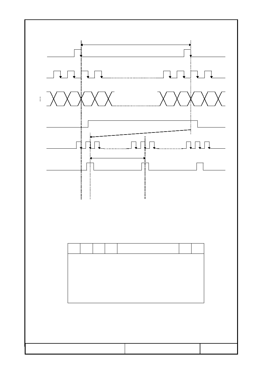
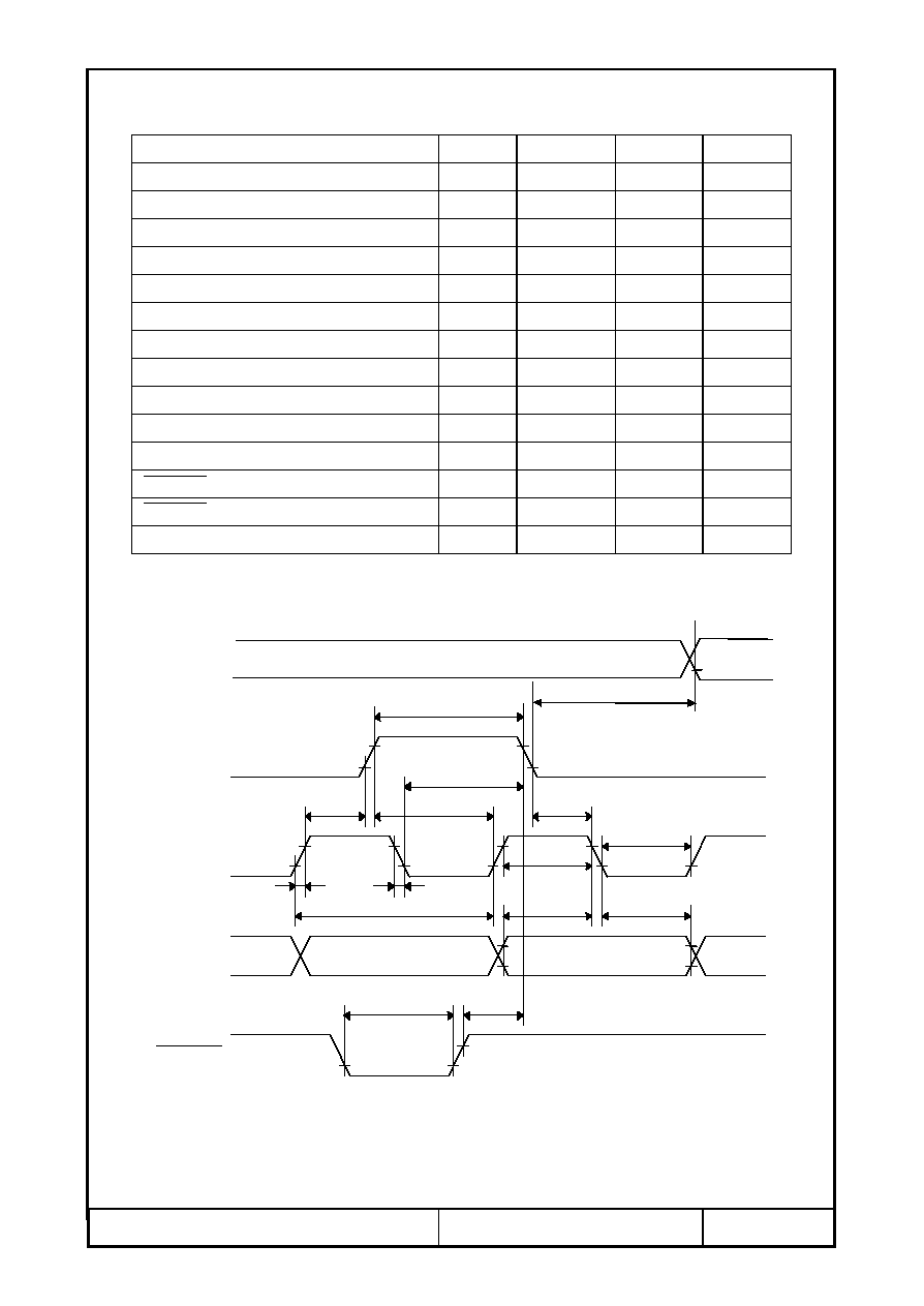
2.3. AC Characteristics
V
CC
=4.5~5.5V
Parameter
Symbol
Min.
Max.
Units
Shift Clock Period
t
WCK
71
-
ns
Shift Clock "H" Pulse Width
t
WCKH
23
-
ns
Shift Clock "L" Pulse Width
t
WCKL
23
-
ns
Data Setup Time
t
DS
10
-
ns
Data Hold Time
t
DH
20
-
ns
Latch Pulse "H" Pulse Width
t
WLPH
15
-
ns
Shift Clock Rise to Latch Pulse Rise Time
t
LD
0
-
ns
Shift Clock Fall to Latch Pulse Fall Time
t
SL
25
-
ns
Latch Pulse Rise to Shift Clock Rise Time
t
LS
25
-
ns
Latch Pulse Fall to Shift Clock Rise Time
t
LH
25
-
ns
Input Signal Rise,Fall Time
t
r,
t
f
-
50 Note.1
ns
DISPOFF Removal Time
t
SD
100
-
ns
DISPOFF Enable Pulse Width
t
WDL
1.2
-
�
s
Output Delay Time
t
DL
-
200 Note.2
ns
Note.1 : (
t
CK �
twckll - twckl)/2 is the maximum in case of high speed operation.
Note.2 : C
L
=15pF
t
WDL
t
SD
tr
tf
t
DH
t
DS
t
WCKL
t
LH
t
SL
CP
t
LD
t
LS
LP
DISPOFF
D0~D3
t
WLPH
TOP DATA
LAST DATA
t
WCK
t
WCKH
TDL
EIO1
(NT7704)