
T-51410D104J-FW-P-AC (AC) No. 2002-0203
OPTREX CORPORATION
Page 1/25
LCD Module Technical Specification
T-51410D104J-FW-P-AC
NO.
ITEM
PAGE
-
Contents
1
1
Application
2
2
Features
2
3
Mechanical Specifications
2
4
Mechanical Drawing of TFT-LCD module
3
5
Input / Output Terminals
4
6
Absolute Maximum Ratings
6
7
Electrical Characteristics
6
8
Power On Sequence
12
9
Optical Characteristics
13
10
Handling Cautions
16
11
Reliability Test
17
12
Indication of Label
17
13
Block Diagram
18
14
Standard
19
15
Packing
24
-
Revision History
25
Checked by (ACI Engineering Div.)
Checked by (Quality Assurance Div.)
Approved by (Production Div.)
Prepared by (Production Div.)
Type No.
Oct 8, 2002
O P T R E X
First Edition
Final Revision
******

T-51410D104J-FW-P-AC (AC) No. 2002-0203
OPTREX CORPORATION
Page 2/25
1.Application
This data sheet applies to a color TFT LCD module, T-51410D104J-FW-P-AC.
T-51410D104J-FW-P-AC module applies to notebook PC, sub-note-book PC and other OA
product, which require high quality flat panel display. This module is not designed for
aerospace, avionics, medical, F/A, transportation, car or any other products, which
require extreme level of reliability.
Prime View assume no responsibility for any damage resulting from the use of the
device which dose not comply with the instructions and the precautions in these specification
sheet.
2. Features
. Amorphous silicon TFT LCD panel with back-light unit
. Pixel in stripe configuration
. Slim and compact, designed for O/A application
. Display Colors:262,144 colors
. Optimum Viewing Direction:6 o'clock
. 3.3V LVDS interface standard: DS90CF364 as receiver
. +3.3V DC supply voltage for TFT LCD panel driving
. Backlight driving DC/AC inverter not included in this module
.Long Life Lamp
3.Mechanical Specifications
Parameter
Specifications
Unit
Screen Size
26.4(diagonal)
cm
10.4 (diagonal)
inch
Display Format
800
�
(R, G, B)
�
600
dot
Display Colors
262,144
Active Area
211.2(H)
�
158.4 (V)
mm
Pixel Pitch
0.264 (H)
�
0.264 (V)
mm
Pixel Configuration
Stripe
Outline Dimension
238.6 (w)
�
171.0(H)
�
6.0(typ.) (D)
mm
Weight
310(typ.),320(max.)
g
Back-light
Single CCFL, side-light type
Surface treatment
Anti-glare and hard-coating
Display mode
Normally white

T-51410D104J-FW-P-AC (AC) No. 2002-0203
OPTREX CORPORATION
Page 3/25
4. Mechanical Drawing of TFT-LCD Module
Unit: mm

T-51410D104J-FW-P-AC (AC) No. 2002-0203
OPTREX CORPORATION
Page 4/25
5. Input Terminals
5-1) TFT-LCD Panel Driving
Connector type: Molex 55177-1491
Pin No.
Symbol
Function
Remark
1
VDD
Power supply : +3.3V
2
VDD
Power supply : +3.3V
3
GND
4
GND
5
IN0-
Pixel data Transmission pair 0 (negative -)
6
IN0+
Pixel data Transmission pair 0 (positive +)
7
IN1-
Pixel data Transmission pair 1 (negative -)
8
IN1+
Pixel data Transmission pair 1 (positive +)
9
IN2-
Pixel data Transmission pair 2 (negative -)
10
IN2+
Pixel data Transmission pair 2 (positive +)
11
CLK-
Sampling Clock (negative -)
12
CLK+
Sampling Clock (positive +)
13
GND
14
GND
Recommended Transmitter (DS90C*363 of National Semiconductor) to
T-51410D104J-FW-P-AC interface Assignment:
Input terminal of DS
90C*363
Graphic controller output signal
Output signal
symbol
To T-51410D104J-
FW-P-AC
Interface
terminal(Symbol)
Symbol
No.
Symbol
Function
TIN0
44
R0
Red pixel data (LSB)
TIN1
45
R1
Red pixel data
TIN2
47
R2
Red pixel data
Tout0-
No.5 : IN0-
TIN3
48
R3
Red pixel data
TIN4
1
R4
Red pixel data
Tout0+
No.6 : IN0+
TIN5
3
R5
Red pixel data(MSB)
TIN6
4
G0
Green pixel data (LSB)
TIN7
6
G1
Green pixel data
TIN8
7
G2
Green pixel data
TIN9
9
G3
Green pixel data
Tout1-
No.7 : IN1-
TIN10
10
G4
Green pixel data
TIN11
12
G5
Green pixel data(MSB)
Tout1+
No.8 : IN1+
TIN12
13
B0
Blue pixel data(LSB)
TIN13
15
B1
Blue pixel data
TIN14
16
B2
Blue pixel data
TIN15
18
B3
Blue pixel data
TIN16
19
B4
Blue pixel data
Tout2-
No.9 : IN2-
TIN17
20
B5
Blue pixel data(MSB)
TIN18
22
NC
No connection
Tout2+
N0.10 : IN2+
TIN19
23
NC
No connection
TIN20
25
ENAB Compound Synchronization signal
CLK in
26
NCLK Data sampling clock
TCLK out-
TCLK out+
No.11 : CLK IN-
No.12 : CLK IN+

T-51410D104J-FW-P-AC (AC) No. 2002-0203
OPTREX CORPORATION
Page 5/25
Data stream of IN0-/+, IN1-/+ and IN2-/+ for T-51410D104J-FW-P-AC
LVDS Interface Block Diagram
Graphic Controller Circuit
TIN0~TIN5
TIN6~TIN11
TIN12~TIN17
TIN18
TIN19
TIN20
TCLK IN
R0~R5
G0~G5
B0~B5
NC
NC
ENAB
CLK IN
TTL parallel to LVDS
PLL
DS90C*363
LVDS to TTL parallel
PLL
DS90CF364
IN0-
IN0+
RxOUT0~RxOUT5
RxOUT6~RxOUT11
RxOUT12~RxOUT17
RxOUT18
RxOUT19
RxOUT20
CLK OUT
LCD Internal Circuit
IN1-
IN1+
IN2-
IN2+
CLK-
CLK+
T-51410D104J-FW-P-AC
module side
Customer system side
5-2) Backlight driving
Connector type : "BHR-02VS-1" of Japan Solderless Terminal MFG Co. LTD
PIN NO.
Symbol
Description
Remark
1
VL1
Input Voltage(High)
2
VL2
Input Voltage(Low)
RxOUT6
RxOUT5
RxOUT4
RxOUT3
RxOUT2
RxOUT1
RxOUT0
G0
R5
R4
R3
R2
R1
R0
IN0
RxOUT13 RxOUT12 RxOUT11 RxOUT10 RxOUT9
RxOUT8
RxOUT7
B1
B0
G5
G4
G3
G2
G1
IN1
RxOUT13 RxOUT12 RxOUT11 RxOUT10 RxOUT9
RxOUT8
RxOUT7
ENAB
NC
NC
B5
B4
B3
B2
IN2
T-51410D104J-FW-P-AC (AC) No. 2002-0203
OPTREX CORPORATION
Page 6/25
6. Absolute Maximum Ratings:
GND=0V, Ta=25
�
C
Parameters
Symbol
MIN.
MAX.
Unit
Remark
Supply Voltage
VDD
-0.3
+4.0
V
Input Signals Voltage
V
IN
-0.3
VDD+0.3
V
Note 6-1
Backlight Driving Voltage
V
L
-
2000
V
Backlight Driving Frequency
F
L
0
100
KHz
Storage Temperature
T
ST
-20
+70
�
C
Note 6-2
Operating Temperature
T
OP
0
+60
�
C
Note 6-1: LVDS signal
Note 6-2: Humidity : 90% RH Max. at Ta
40
Maximum wet-bulb temperature is at 39,or less at Ta > 40,and no condensation.
7. Electrical Characteristics
7-1) Recommended Operating Conditions:
GND = 0V,Ta = 25
�
C
Item
Symbol
Min.
Typ.
Max.
Unit
Remark
Supply Voltage
VDD
3.0
3.3
3.6
V
Current Dissipation
I
DD
-
350
450
mA
Note 7-1
LVDS Differential input high threshold
V
TH
-
-
100
mV
Note 7-2
LVDS Differential input low threshold
V
TL
-100
-
-
Lamp Current
I
FL
3.0
5.0
6.0
mA 5mA : 160 cd/m2
Note 7-3
Note 7-5
Lamp Voltage
V
L
500
550
600
Vrms
I
FL
=5mA
Note 7-3
Lamp Initial Voltage
V
SFL
-
1200
-
Vrms
at Ta=25
�
C
1000
at Ta=0
�
C
Lamp Driving Frequency
F
L
-
45
-
KHz
Total power consumption (at I
FL
=5mA)
--
3.91
-
W
Note 7-4
Note 7-1: To test the current dissipation of VDD, using the "color bars" testing pattern shown
as below.
1
2
3
4
5
6
7
8
1.
White
2.
Yellow
3.
Cyan
4.
Green
5.
Magenta
6.
Red
7.
Blue
8.
Black
Idd current dissipation testing pattern

T-51410D104J-FW-P-AC (AC) No. 2002-0203
OPTREX CORPORATION
Page 7/25
Note 7-2: Please refers to DS90CF364 specification by National Semiconductor Corporation.
This LCD module conforms to LVDS standard.
Note 7-3: The back-light driving waveform should be as closed to sine-wave as possible.
In order to satisfy the quality of B/L , no matter use what kind of inverter , the output
lamp current must between Min. and Max. to avoid the abnormal display imagecaused by B/L.
Note 7-4: Not including the efficiency of backlight DC/AC inverter
Note 7-5: Lamp current is measured with current meter for high frequency as shown below
Inverter
TFT-LCD
Module
~
A
1
2
* Pin 2 is V
low
** Current meter :
Yokogawa 2016-01
7-2) Input / Output signal timing chart
(A) Vertical Timing
X,1
X,2
X,3 X,4
X,598 X,599 X,600
X,Y
t
1
t
2
t
3
t
3
CLK
ENAB
R5~R0
G5~G0
B5~B0
Lamp current dissipation testing configuration

T-51410D104J-FW-P-AC (AC) No. 2002-0203
OPTREX CORPORATION
Page 8/25
(B) Horizontal Timing
t
3
t
4
t
c
CLK
ENAB
R5~R0
G5~G0
B5~B0
1,Y 2,Y 3,Y 4,Y 5,Y 6,Y 7,Y
X,Y
798,Y 800,Y
797,Y 799,Y
CLK
t 6
t 7
t 5
V
IH
(Min):0.8V
cc
V
IL
(Max):0.2V
cc
ENAB
R5-R0
G5-G0
B5-B0
VALID
DATA
Input Signal
CenterLevel:
0.5V
cc
V
IH
(Min):0.8V
cc
V
IL
(Max):0.2V
cc
CLK
a
b
0.5V
cc
Duty
a ,b
: 50�10%
t 8
t 9

T-51410D104J-FW-P-AC (AC) No. 2002-0203
OPTREX CORPORATION
Page 9/25
D) Timing Specifications
Item
Symbol
Min.
Typ.
Max.
Unit Remark
Frame Cycling
t1
604
�
t3
628
�
t3
660
�
t3
-
-
16.58
17.86
ms
Vertical Display Period
t2
600
�
t3
600
�
t3
600
�
t3
-
Horizontal Scanning Time
t3
844
�
t5
1056
�
t5
1064
�
t5
-
26.3
26.4
-
s
Horizontal Display Period
t4
-
800
�
t5
-
-
Clock Cycle
t5
24.0
25.0
-
ns
Clock High Level Time
t6
9.0
-
-
ns
Clock Low Level Time
t7
9.0
-
-
ns
Hold time
t8
4.0
-
-
ns
Set-up time
t9
5.0
-
-
ns
T-51410D104J-FW-P-AC (AC) No. 2002-0203
OPTREX CORPORATION
Page 10/25
7-3) Display Color and Gray Scale Reference
Input Color Data
Color
Red
Green
Blue
R5 R4 R3 R2 R1 R0 G5 G4 G3 G2 G1 G0 B5 B4 B3 B2 B1 B0
Black
0 0 0 0 0 0 0 0 0 0 0 0 0 0 0 0 0 0
Red (63)
1 1 1 1 1 1 0 0 0 0 0 0 0 0 0 0 0 0
Green (63) 0 0 0 0 0 0 1 1 1 1 1 1 0 0 0 0 0 0
Basic
Blue (63)
0 0 0 0 0 0 0 0 0 0 0 0 1 1 1 1 1 1
Colors
Cyan
0 0 0 0 0 0 1 1 1 1 1 1 1 1 1 1 1 1
Magenta
1 1 1 1 1 1 0 0 0 0 0 0 1 1 1 1 1 1
Yellow
1 1 1 1 1 1 1 1 1 1 1 1 0 0 0 0 0 0
White
1 1 1 1 1 1 1 1 1 1 1 1 1 1 1 1 1 1
Red (00)
0 0 0 0 0 0 0 0 0 0 0 0 0 0 0 0 0 0
Red (01)
0 0 0 0 0 1 0 0 0 0 0 0 0 0 0 0 0 0
Red (02)
0 0 0 0 1 0 0 0 0 0 0 0 0 0 0 0 0 0
Darker
Red
Brighter
Red (61)
1 1 1 1 0 1 0 0 0 0 0 0 0 0 0 0 0 0
Red (62)
1 1 1 1 1 0 0 0 0 0 0 0 0 0 0 0 0 0
Red (63)
1 1 1 1 1 1 0 0 0 0 0 0 0 0 0 0 0 0
Green (00) 0 0 0 0 0 0 0 0 0 0 0 0 0 0 0 0 0 0
Green (01) 0 0 0 0 0 0 0 0 0 0 0 1 0 0 0 0 0 0
Green (02) 0 0 0 0 0 0 0 0 0 0 1 0 0 0 0 0 0 0
Darker
Green
Brighter
Green (61) 0 0 0 0 0 0 1 1 1 1 0 1 0 0 0 0 0 0
Green (62) 0 0 0 0 0 0 1 1 1 1 1 0 0 0 0 0 0 0
Green (63) 0 0 0 0 0 0 1 1 1 1 1 1 0 0 0 0 0 0
Blue (00)
0 0 0 0 0 0 0 0 0 0 0 0 0 0 0 0 0 0
Blue (01)
0 0 0 0 0 0 0 0 0 0 0 0 0 0 0 0 0 1
Blue (02)
0 0 0 0 0 0 0 0 0 0 0 0 0 0 0 0 1 0
Darker
Blue
Brighter
Blue (61)
0 0 0 0 0 0 0 0 0 0 0 0 1 1 1 1 0 1
Blue (62)
0 0 0 0 0 0 0 0 0 0 0 0 1 1 1 1 1 0
Blue (63)
0 0 0 0 0 0 0 0 0 0 0 0 1 1 1 1 1 1

T-51410D104J-FW-P-AC (AC) No. 2002-0203
OPTREX CORPORATION
Page 11/25
7-4) Pixel Arrangement
The LCD module pixel arrangement is the stripe.
R G B R G B R G B
R G B
R G B R G B
R G B
R G B R G B R G B
R G B
R G B R G B
R G B
3
rd Line
2 nd Line
1
st Line
600 th Line
599 th Line
598 th Line
R G B
R G B
R G B
R G B
1 st Pixel
800 th Pixel
1 Pixel = R G B

T-51410D104J-FW-P-AC (AC) No. 2002-0203
OPTREX CORPORATION
Page 12/25
8.Power On Sequence
1. The supply voltage for input signals should be same as V
CC.
2. When the power is off , please keep whole signals (Hsync, Vsync, CLK, Data) low level
or high impedance
3.0 V
3.0 V
0 s< t <35 ms
0 s< t <35 ms
2t
1
0<t
1
Signal
Backlight
V
CC

T-51410D104J-FW-P-AC (AC) No. 2002-0203
OPTREX CORPORATION
Page 13/25
9. Optical Characteristics
9-1) Specification:
Ta = 25
�
C
Parameter
Symbol Condition
MIN. TYP. MAX. Unit
Remarks
Horizontal
�
35
�
45
-
deg
(to 12
o'clock)
10
15
-
deg Note 9-1
Viewing Angle
Vertical
(to 6
o'clock)
CR
10
25
40
-
deg
Contrast Ratio
CR
Optimum
direction
100
180
-
-
Note 9-2
Rise
Tr
-
15
50
ms
Response time
Fall
Tf
=0
�
=0
�
-
25
50
ms
Note 9-4
Luminance
L
=0
�
/
=0
�
130
160
-
cd/m
2
I
FL
=5mA, Note 9-3
Luminance Uniformity
U
55
80
-
%
Note 9-5
x
0.260 0.310 0.360
-
y
0.290 0.340 0.390
-
White Chromaticity
Tc
6400 6600
6800
K
Lamp Life Time
30000 40000
-
hr
I
FL
=5mA
Cross Talk Ratio
CTK
-
-
3.5
%
Note 9-6
All the optical measurement shall be executed 30 minutes after backlight being turn-on. The optical
characteristics shall be measured in dark room (ambient illumination on panel surface less than 1
Lux). The measuring configuration shows as following figure.
Photometer (TOPCON
BM-5A or BM-7 fast)
500 mm +/- 50 mm
TFT-LCD module
DC/AC Invert
er
Optical characteristics measuring configuration
Field = 2
�

T-51410D104J-FW-P-AC (AC) No. 2002-0203
OPTREX CORPORATION
Page 14/25
Note 9-1': The definitions of viewing angles are as follows.
12 o'clock
3 o'clock
9 o'clock
6 o'clock
Lamp connector
Note 9-2: The definition of contrast ratio
0
level
gray
at
Luminance
63
level
gray
at
Luminance
CR
=
Note 9-3: Topcon BM-5A luminance meter 2
�
field of view is used in the testing (after 30 minutes'
operation). The typical luminance value is measured at lamp current 3.0 mA. The max
luminance value is measured at lamp current 6.0 mA.
Note 9-4: Definition of Response Time T
r
and T
f
:
100%
90%
10%
0%
White
White
B
r
i
g
h
t
n
e
s
s
Black
Tr
Tf
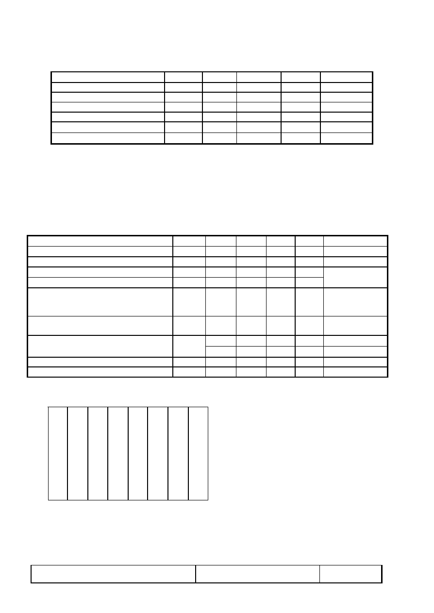
Note 9-5: The uniformity of LCD is defined as
The Minimum Brightness of the 9 testing Points
U =
The Maximum Brightness of the 9 testing Points
Luminance meter : BM-5A or BM-7 fast(TOPCON)
Measurement distance : 500 mm +/- 50 mm
Ambient illumination : < 1 Lux
Measuring direction : Perpendicular to the surface of module
T-51410D104J-FW-P-AC (AC) No. 2002-0203
OPTREX CORPORATION
Page 15/25
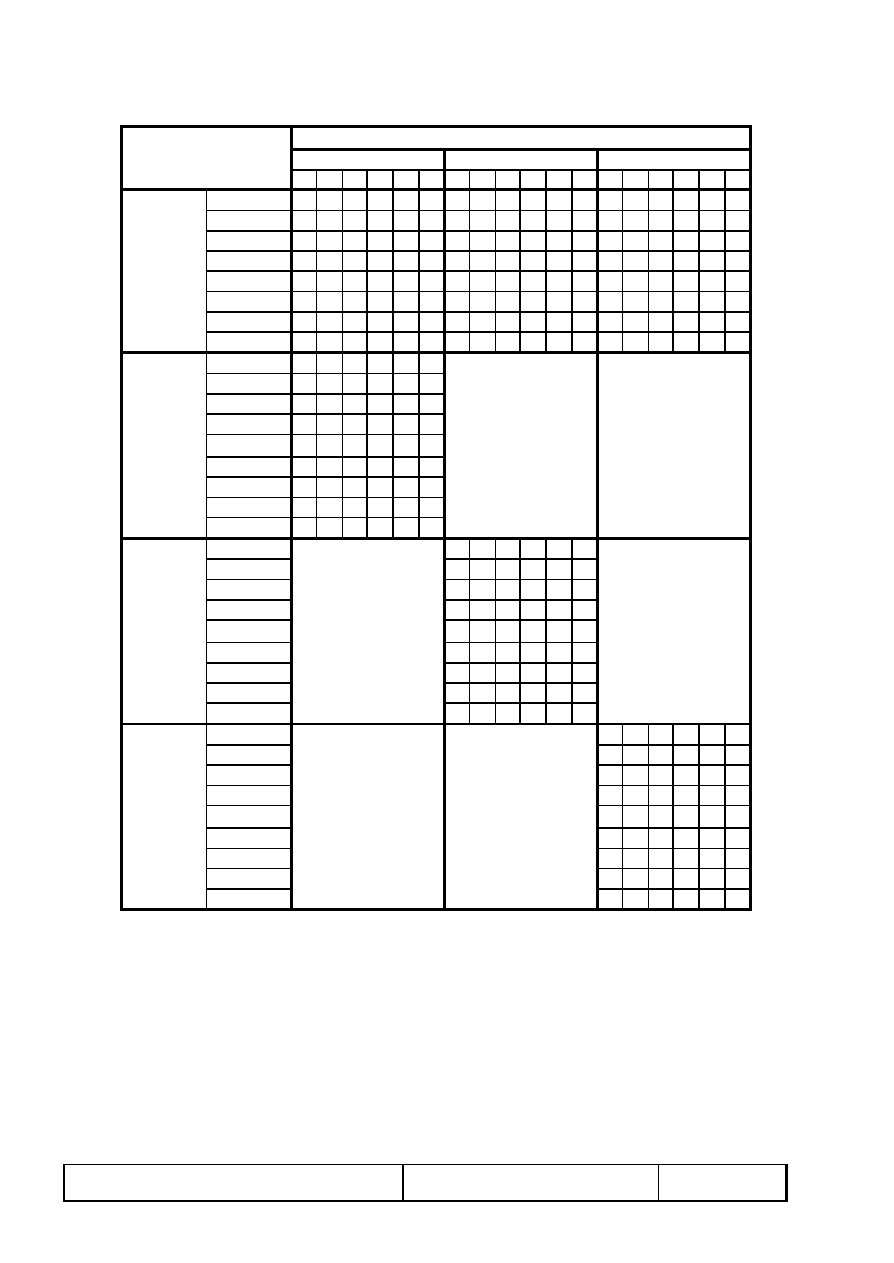
The test pattern is white (Gray Level 63).
25%
50%
75%
25%
50%
75%
YA-YB
Note 8-6: Cross Talk (CTK) =
YA
�100%
YA: Brightness of Pattern A
YB: Brightness of Pattern B
Luminance meter: BM 5A (TOPCON)
Measurement distance: 500 mm +/- 50 mm
Ambient illumination: < 1 Lux
Measuring direction: Perpendicular to the surface of module
Pattern A
(Gray Level 31)
Pattern B
(Gray Level 31, central
black box exclusive)
: Measuring Point (A and B are at the same point.)
YA
YB
1/3
1/3
1/3
1/3
1/3
1/3
Black
(Gray Level 0)

T-51410D104J-FW-P-AC (AC) No. 2002-0203
OPTREX CORPORATION
Page 16/25
10. Handling Cautions
10-1) Mounting of module
a) Please power off the module when you connect the input/output connector.
b) Please connect the ground pattern of the inverter circuit surely. If the connection
is not perfect, some following problems may happen possibly.
1.The noise from the backlight unit will increase.
2.The output from inverter circuit will be unstable.
3.In some cases a part of module will heat.
c) Polarizer which is made of soft material and susceptible to flaw must be
handled carefully.
d) Protective film (Laminator) is applied on surface to protect it against scratches
and dirts. It is recommended to peel off the laminator before use and taking
care of static electricity.
10-2) Precautions in mounting
a) When metal part of the TFT-LCD module (shielding lid and rear case) is soiled,
wipe it with soft dry cloth.
b) Wipe off water drops or finger grease immediately. Long contact with water may
cause discoloration or spots.
c) TFT-LCD module uses glass which breaks or cracks easily if dropped or bumped
on hard surface. Please handle with care.
d) Since CMOS LSI is used in the module. So take care of static electricity and
earth yourself when handling.
10-3) Adjusting module
a) Adjusting volumes on the rear face of the module have been set optimally before
shipment.
b) Therefore, do not change any adjusted values. If adjusted values are changed,
the specifications described may not be satisfied.
10-4) Others
a) Do not expose the module to direct sunlight or intensive ultraviolet rays for many
hours.
b) Store the module at a room temperature place.
c) The voltage of beginning electric discharge may over the normal voltage because
of leakage current from approach conductor by to draw lump read lead line
around.
d) If LCD panel breaks, it is possibly that the liquid crystal escapes from the panel.
Avoid putting it into eyes or mouth. When liquid crystal sticks on hands, clothes
or feet. Wash it out immediately with soap.
e) Observe all other precautionary requirements in handling general electronic
components.
f) Please adjust the voltage of common electrode as material of attachment by 1
module.

T-51410D104J-FW-P-AC (AC) No. 2002-0203
OPTREX CORPORATION
Page 17/25
11. Reliability Test
No
Test Item
Test Condition
Remark
1 High Temperature Storage Test
Ta = +70
�
C, 240 hrs
2 Low Temperature Storage Test
Ta = -20
�
C, 240 hrs
3 Low Temperature Operation Test
Ta = 0
�
C, 240 hrs
4
High Temperature & High Humidity
Operation Test
Ta = +60
�
C, 80%RH, 240 hrs
(No Condensation)
5
Thermal Cycling Test
(non-operating)
0
�
C
��
+25
�
C
��
+60
�
C, 50 Cycles
1Hr 0.5Hr 1Hr
6
Vibration Test
(non-operating)
Frequency:10
57 H
Z ,
Amplitude: 0.15 mm
58
500Hz, 1G
Sweep time: 11 min
Test Period: 3 hrs(1 hr for each direction of X, Y,
Z)
7
Shock Test
(non-operating)
80G, 6ms, X,Y, Z
1 times for each direction
Ta: ambient temperature
[Judgement Criteria]
Under the display quality test conditions with normal operation state , there should be no
change which may affect practical display function.
12. Indication of Label
a) Indicated contents of the label
Lot number
Products number
Contents of lot number : 1st--Process area : class 1000
H
class 100K
M
2nd~3rd--Module screen size(in inch) : 1.8"
18, 2.5"
25......
5th--Production year : 1999
9, 2000
A, 2001
1........
6th--Production month : 1, 2, 3,....9, A, B, C
7th~10th--Serial numbers : 0001~9999
b) Indicated contents of the Product number label
T-51382D064J-FW-P-AC
MADE IN TAIWAN
XXXXXXXXXXXXXXXXXXXXX
Module Name of Optrex
Ex. T-51382D064J-FW-P-AC
Barcode Symbol
Barcode Number
Production Country
The Module Manufacture Location
OOO-OOOOOO
OD104SL3XX

T-51410D104J-FW-P-AC (AC) No. 2002-0203
OPTREX CORPORATION
Page 18/25
13. Block Diagram
1
2
3
5 9 9
5 9 8
6 0 0
4
2
1
2 4 0 0
C
o
n
t
r
o
l
C
i
r
c
u
i
t
E N AB
C L K
I N 0 -/ +
I N 1 -/ +
I N 2 -/ +
T F T -L C D
D is p la y A re a
B a c k -lig h t (L a m p 1 )
V L 1
V L 2
3
S o u rc e D riv e r
G
a
t
e
D
r
i
v
e
r
L
V
D
S
I
n
t
e
r
f
a
c
e
(
D
S
9
0
C
3
6
4
)
P o w er
M o d u le
V D D
E N A B
C L K
R 0
R 1
G 0
G 1 1
B 0
B 1
R 5
G 5
B 5
...
...
...

T-51410D104J-FW-P-AC (AC) No. 2002-0203
OPTREX CORPORATION
Page 19/25
14. Standard
14-1) Inspection condition
Viewing Angle (Major axis x)
< 45
�
inspection under non-operating condition
< 5
�
inspection under operating condition
TFT-LCD Module
Back-Light Unit
35cm or more
Viewing Zone
14-2) Environment condition
�
Ambient Temperature: 25
�
C
�
5
�
C
�
Ambient Humidity: 65
�
5%RH
�
Ambient Luminance: 20 watts fluorescent lamp (about 500 lux)
14-3) Sampling condition
Unless otherwise agreed in written, the sampling inspection shall be applied
to the incoming inspection of customer.
�
Lot size: Quantity of shipment lot per model.
�
Sampling type: Normal inspection, single sampling
�
Sampling Level: Level II
�
Sampling table: ISO 2859 (Also known as MIL-STD-105E).
14-4) Acceptance Quality Level (AQL)
The AQL for major and minor defects is defined as follows:
�
Major defect: 0.65%
�
Minor defect: 1.5%
14-5) Classification of defects
Defects and classified as either a major or minor defect defined as bellows:
�
Major defect:
It is a defect that is likely to result in failure or to reduce materially the
usability of the product for the intended function.
�
Minor defect:

T-51410D104J-FW-P-AC (AC) No. 2002-0203
OPTREX CORPORATION
Page 20/25
It is a defect that will not result in functioning problem with deviation classified.
14-6) Inspection Instrument:
�
DC Power supply: DC 12V
�
Luminance color meter: Topcon BM �7
�
Others: Micrometer, Microscope, and Caliper.

T-51410D104J-FW-P-AC (AC) No. 2002-0203
OPTREX CORPORATION
Page 21/25
14-7) Cosmetic Specification
Item
Specification/Description
Classification
Note
Display function
No Display
Malfunction
Major
Flickering
Visible at display area
Minor
Contrast ratio
(Black, White)
Does not meet specified
range in the spec.
Major
Line defect
Vertical and Horizontal
Line defect in bright, dark
Major
Point defect
(Red, Green, Blue,
Dark)
Minor
1
Image retention
After displaying fixed
pattern for 30 minutes,
the afterimage is visible
after 10 seconds.
Minor
Display
Inspection
(operating)
Non-uniformity
Visible through 2 % ND
Filter.
Minor
Dimension
Outline
Major
Bezel appearance
Out of mechanical spec
regarding bending area.
Minor
Scratch on the
polarizer
N=5 max (W
0.1 or L
10)
N=0 (W>0.1 or L>10)
Minor
2
Dent or Bubble on
the polarizer
( in available
viewing area )
N=5 max (W
0.5 and L
10)
N=0 (W>0.5 or L>1.0)
Minor
2
Foreign material
on polarizer
(W >1/4L)
N=4 max (0.1L<D
0.4)
N disregard
(W
1/4L)
N=4 max (0.03 <W
0.10
and 0.3<L
2.1)
N=0 (W>0.1orL>2.1)
Minor
3
Plastic frame
Break or modification
Minor
2
External
Inspection
(non-operating)
Wrinkle on
polarizer
Serious wrinkle is not
allowed
Item
Number Total
Bright
(Green)
3
Bright
10
10
Dark
10
12

T-51410D104J-FW-P-AC (AC) No. 2002-0203
OPTREX CORPORATION
Page 22/25
Cable
The metal wire is exposed
Minor
2
Connector
(signal input)
Break
Major
(W-Width in mm, L-Length in mm, N-Number, D-Average Diameter in mm,)
Remark: Major: Defect that is likely to result in failure or to reduce materially the
usability of the product for the intended function.
Minor: Defect that will not result in functioning problem with deviation
as classified.
T-51410D104J-FW-P-AC (AC) No. 2002-0203
OPTREX CORPORATION
Page 23/25
Note: 1. (a) Bright point defect is defined as point defect of R, G, B with area >1/2 pixel
Respectively and is not visible by using 5% ND filter.
(b) Definition of distribution of point defect is as follows:
within 20mm diameter, it is allowed 4 dark points or 3 bright and dark points max.
(c) Definition of joined bright point defect is as follows:
-Three joined bright point must be nil.
-Joined bright point is 3 pairs maximum.
(d) Definition of joined dark point defect is as follows:
-Three jointed dark point must be nil.
-Coupling of one dark and one bright point in junction is counted as one dark and
one bright spot.
-Two dark point in junction is counted as one dark point.
Note: 2. The external inspection is conducted at the distance 30cm minimum between the
eyes of inspector and the panel. The inspection area is defined as full screen.
Note: 3. W: Width of foreign material
L: Length of foreign material (Take larger value of L
1
and L
2
)
4A:

T-51410D104J-FW-P-AC (AC) No. 2002-0203
OPTREX CORPORATION
Page 24/25
15. Packing

T-51410D104J-FW-P-AC (AC) No. 2002-0203
OPTREX CORPORATION
Page 25/25
Revision History
Rev.
Issued Date
Revised Content
1.0 Apr. 03, 2002 New
1.1 Jun. 03, 2002 Add
Page 18 : Indication of Lot Number Label