 | –≠–Ľ–Ķ–ļ—ā—Ä–ĺ–Ĺ–Ĺ—č–Ļ –ļ–ĺ–ľ–Ņ–ĺ–Ĺ–Ķ–Ĺ—ā: F0496A | –°–ļ–į—á–į—ā—Ć:  PDF PDF  ZIP ZIP |
F 0496A
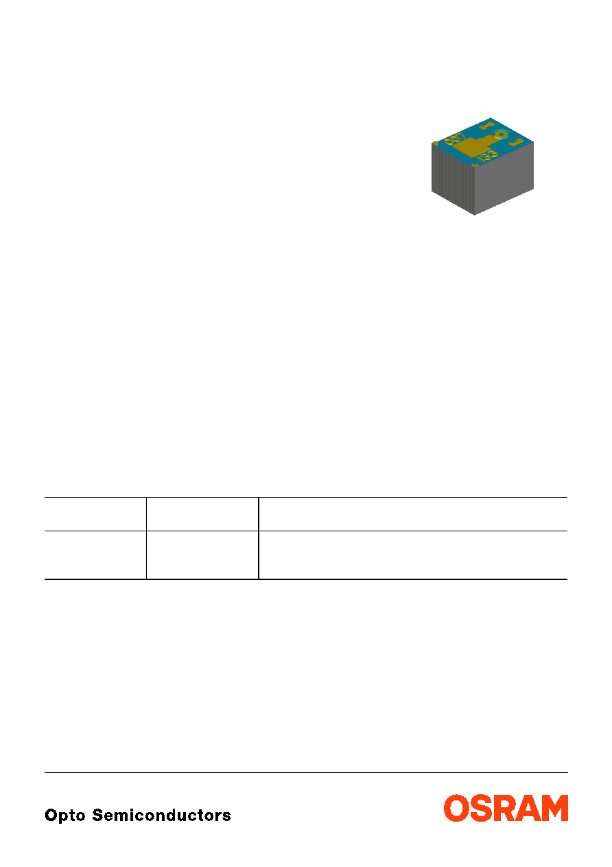
GaAs-Infrarot-VCSEL-Chip (850 nm)
GaAs Infrared VCSEL Chip (850 nm)
Vorlšufige Daten / Preliminary Data
2003-03-26
1
Wesentliche Merkmale
∑ Technologie basierend auf selektiver Oxidation
∑ Sehr hohe Datenrate (GBit/s) mŲglich
∑ Oberflšchenstrahler
∑ Emissionswellenlšnge 850nm
∑ Multimodebetrieb
∑ Zuverlšssigkeit gemšŖ Bellcore Standard
Anwendungen
∑ Faseroptische DatenŁbertragung
∑ Parallel optical data link
∑ Laserdrucker
∑ Nšherungssensoren
∑ Reflexlichtschranken
∑ Gabellichtschranken
Typ
Type
Bestellnummer
Ordering Code
Beschreibung
Description
F 0496A
on request
Infrarot emittierender VCSEL-Chip, Oberseite Anodenan-
schluss
Infrared emitting VCSEL die, top side anode connection
Features
∑ Technology based on selective oxidation
∑ Very high data rate (GBit/s) possible
∑ Surface emitter
∑ 850 nm emission wavelength
∑ Multimode operation
∑ Reliability acc. Bellcore Standard
Applications
∑ Fiber Optic data link
∑ Parallel optical data link
∑ Laser printing
∑ Proximity sensors
∑ Reflective sensor
∑ Slotted interrupter

2003-03-26
2
F 0496A
Elektrische Werte (gemessen auf TO18-Bodenplatte ohne Verguss,
T
A
= 25
į
C)
Electrical values (measured on TO18 header without resin,
T
A
= 25
į
C)
Bezeichnung
Parameter
Symbol
Symbol
Wert
1)
Value
1)
Einheit
Unit
min.
typ.
max.
Wellenlšnge der Strahlung
Wavelength at peak emission
I
F
= 10 mA
peak
830
850
870
nm
Spektrale Bandbreite bei 50% von
I
max,
I
F
= 10 mA
Spectral bandwidth at 50% of
I
max
0.7
nm
Schwellstrom
Threshold current
th
1
3
5
mA
Steilheit
Slope efficiency
0.2
0.25
0.4
mW/mA
Schaltzeiten,
I
e
von 10% auf 90% und von
90% auf 10%, bei
I
F
= 6 mA,
R
L
= 50
Switching times,
I
e
from 10% to 90% and from
90% to 10%,
I
F
= 6 mA,
R
L
= 50
t
r
,
t
f
200
ps
Durchla
spannung
Forward voltage
I
F
= 10 mA,
t
p
= 20 ms
V
F
1.7
2.1
2.5
V
Dynamischer Widerstand
Dynamic Resistance
R
S
30
60
100
V
Sperrstrom
Reverse current
V
R
= 3 V
I
R
0.01
Ķ
A
Gesamtstrahlungsflu
4)
Total radiant flux
4)
I
F
= 10 mA,
t
p
= 20 ms
e
1.5
1.8
mW
Detuning
T
opt
10
25
40
įC
Temperaturkoeffizient von
peak
,
I
F
= 10 mA
Temperature coefficient of
peak
,
I
F
= 10 mA
TC
0.06
nm/K

F 0496A
2003-03-26
3
Mechanische Werte
Mechanical values
Bezeichnung
Parameter
Symbol
Symbol
Wert
1)
Value
1)
Einheit
Unit
min.
typ.
max.
Chipkantenlšnge (x-Richtung)
Length of chip edge (x-direction)
L
x
0.25
0.27
0.29
mm
Chipkantenlšnge (y-Richtung)
Length of chip edge (y-direction)
L
y
0.20
0.22
0.24
mm
Durchmesser der aktiven Chipflšche
Dimension of the active chip area
D
15
Ķm
Durchmesser des Wafers
Diameter of the wafer
D
76.2
mm
ChiphŲhe
Die height
H
160
185
210
Ķm
Grenzwerte
3)
(
T
A
= 25
į
C)
Maximum Ratings
3)
Bezeichnung
Parameter
Symbol
Symbol
Werte
Value
Einheit
Unit
Betriebs- und Lagertemperatur
Operating and storage temperature range
T
op
;
T
stg
≠ 40
...
+ 85
į
C
Sperrspannung
Reverse voltage
V
R
3
V
DurchlaŖstrom
Forward current
I
F
20
mA

F 0496A
2003-03-26
4
Relative Spectral Emission
2)
I
rel
=
f
(
)
Forward Current
2)
I
F
=
f
(
V
F
)
Optical power
2)
rel
=
f
(
T
)
OHF00141
0
840
nm
rel
860
850
20
40
60
80
100
120
%
OHF00143
0
I
F
F
V
10
-3
-2
10
-1
10
10
0
10
1
10
2
mA
0.5
1
1.5
2
2.5
V
OHF01179
-20
P
opt
T
0
mW
įC
0
20
40
60
100
0.2
0.4
0.6
0.8
1.0
1.2
1.4
1.8
Radiant Intensity
2)
Threshold Current
2)
,
th
=
f
(
T
)
F
ar Field Emission Pattern
2)
e
e
10 mA
=
f
(
I
F
)
OHF00142
0
0
mA
e rel
10
0.2
0.4
0.6
0.8
1.0
1.2
2
4
6
8
F
I
OHF00145
0
I
th
A
T
20
40
60
80
100
įC
0
0.5
1.0
1.5
2.0
2.5
3.0
3.5
4.0
mA
OHF01180
-30
a.u.
-20
-10
0
10
Deg 30
I
4 mA
8 mA
10 mA
15 mA
Near Field Emission Pattern
2)
Spectral Width
2)
FWHM
=
f
(
T)
OHF01182
I
X
a.u.
8 mA
10 mA
15 mA
4 mA
6 mA
a.u.
OHF01181
0
FWHM
T
0
įC
20
40
60
80
100
5
10
15
20
25
Deg

2003-03-26
5
F 0496A
MaŖzeichnung
Chip Outlines
MaŖe werden als typische
1)
Werte wie folgt angegeben: mm (inch) / Dimensions are specified as typical
1)
values as
follows: mm (inch).
GMOY6074
0.185 (0.0073)
0.22 (0.0087)
0.27 (0.0106)
Active area
Bonding area
Bonding area
Active area
p
n