 | –≠–ª–µ–∫—Ç—Ä–æ–Ω–Ω—ã–π –∫–æ–º–ø–æ–Ω–µ–Ω—Ç: F2001A | –°–∫–∞—á–∞—Ç—å:  PDF PDF  ZIP ZIP |
F 1998A
InGaAlP-High Brightness-Lumineszenzdiode (630 nm, High Optical Power)
InGaAlP High Brightness Light Emitting Diode (630 nm, High Optical Power)
Vorl‰ufige Daten / Preliminary Data
2003-04-08
1
Wesentliche Merkmale
∑
Optimierte Lichtauskopplung durch
Oberfl‰chenstrukturierung und Stromverteilung
∑
Chipgrˆþe 300 x 300
µ
m
2
∑
Wellenl‰nge (typ.): 630 nm
∑
Technologie:InGaAIP
∑
Typ. Lichtfluþ: 2 lm @ 70 mA (gepulst, im
Power TOPLED
Æ
Geh‰use).
Anwendungen
∑
Ampeln
∑
Optischer Indikator
∑
Hinterleuchtung (LCD, Handy, Schalter,
Tasten, Displays, Werbebeleuchtung,
Allgemeinbeleuchtung)
∑
Beleuchtung im Automobilbereich
(z.B. Instrumentenbeleuchtung, Bremslichter
und Blinklichter)
∑
Ersatz von Kleinst-Gl¸hlampen
∑
Markierungsbeleuchtung
∑
Signal- und Symbolleuchten
Typ
Type
Bestellnummer
Ordering Code
Beschreibung
Description
F 1998A
Q-67220-C1446
Superrot emittierender Chip mit optimierter Lichtauskopp-
lung durch Oberfl‰chenstrukturierung, Oberseite Anoden-
anschluss
Superred emitting chip with optimized light extraction due to
surface structuring, top side anode connection
Feature
∑ Optimized light extraction due to surface
structuring and current distribution
∑ Chip size 300 x 300
µ
m
2
∑ Wavelength (typ.): 630 nm
∑ Technology: InGaAIP
∑ Typ. luminous flux: 2 lm @ 70 mA (pulsed, in
Power TOPLED
Æ
package)
Applications
∑ Traffic lights
∑ optical indicators
∑ Backlighting (LCD, cellular phones, switches,
keys, displays, illuminated advertising,general
lighting)
∑ Automotive lighting (e.g. dashboard
backlighting, brake lights, turn signal lamps,
etc.)
∑ Substitution of micro incandescent lamps
∑ Marker lights
∑ Signal and symbol luminaire
2003-04-08
2
F 1998A
Elektrische Werte (
T
A
= 25
∞
C)
Electrical values
1)
(
T
A
= 25
∞
C)
Bezeichnung
Parameter
Symbol
Symbol
Wert
Value
2)
Einheit
Unit
min.
typ.
max.
Dominantwellenl‰nge
Dominant wavelength
I
F
= 50 mA, t
p
= 1.8 ms
dom
628
638
nm
Sperrspannung
Reverse voltage
I
R
= 10
µ
A
V
R
12
V
Durchla
spannung
Forward voltage
I
F
= 50 mA, t
p
= 1.8 ms
V
F
2.5
V
Lichtstrom
Luminous Flux
3)
I
F
= 50 mA, t
p
= 1.8 ms
V
650
mlm
1)
Measurement limits describe actual settings and do not include measurement uncertainties. Each wafer and fragment
of a wafer is subject to final testing. The wafer or its pieces are individually attached on foils (rings). Sample chips are
picked from each foil and placed on a special carrier for measurement purposes.
Sample-test: Sampling density/samples per cm≤ (grid): 1,6/cm≤.
If a sample fails, the distance area to the next non-failure samples is manually removed by a vacuum tool.
All el. values are referenced to the vendor's measurement system (correlation to customer product(s) is required)
2)
Typical (refered to as typ.) data are defined as long-term production mean values and are only given for information.
This is not a specified value
3)
Luminous Flux is measured in integrating sphere.
F 1998A
2003-04-08
3
Mechanische Werte
Mechanical values
Bezeichnung
Parameter
Symbol
Symbol
Wert
Value
1)
Einheit
Unit
min.
typ.
max.
Chipkantenl‰nge (x-Richtung)
Length of chip edge (x-direction)
L
x
0.28
0.3
0.32
mm
Chipkantenl‰nge (y-Richtung)
Length of chip edge (y-direction)
L
y
0.28
0.3
0.32
mm
Durchmesser des Wafers
Diameter of the wafer
D
100
mm
Chiphˆhe
Die height
H
200
220
240
µm
Bondpaddurchmesser
Diameter of bondpad
d
109
114
119
µm
Weitere Informationen
Additional information
2)
Vorderseitenmetallisierung
Metallization frontside
Aluminium
Aluminum
R¸ckseitenmetallisierung
Metallization backside
Goldlegierung
Gold alloy
Trennverfahren
Dicing
S‰gen
Sawing
Verbindung Chip - Tr‰ger
Die bonding
Kleben
Epoxy bonding
1)
Typical (refered to as typ.) data are defined as long-term production mean values and are only given for information.
This is not a specified value
2)
All chips are checked according to the following procedure and the OSRAM OS specification of the visual inspection
A63501-Q0013-N001-*-76G3:
The visual inspection shall be made in accordance to the "specification of the visual inspection" as referenced.The
visual inspection of chip backside is performed with stereo microscope with incident light with 40x-80x magnification.
Areas > º cm≤ which have an amount of more than 3% failed dies will be removed. The visual inspection of chip
frontside is performed by a stereo microscope with incident light with 40x-80x magnification for 100% of the area of
each wafer. Areas > 1 cm≤ which have an amount of more than 50% failed dies and areas > 2 cm≤ which have an
amount of more than 25% failed dies will be removed. In areas with failure density higher than 1% each failure die is
inked individually. n request the visual inspection of chip frontside can be performed by an automated visual inspection
combined with automated inking additionally. The quality inspection (final visual inspection) is performed by
production. An additional visual inspection step as special release procedure by QM after the final visual inspection
is not installed.
F 1998A
2003-04-08
4
fj
Grenzwerte
1)
Maximum Ratings
Bezeichnung
Parameter
Symbol
Symbol
Wert
Value
Einheit
Unit
Maximaler Betriebstemperaturbereich
Maximum Operating temperature range
T
op
-40...+100
∞C
Maximaler Lagertemperaturbereich
Maximum storage temperature range
T
stg
-40...+100
∞C
Maximaler Durchlaþstrom (T
A
= 25∞C)
Maximum forward current (T
A
= 25∞C)
I
F
70
mA
Maximaler Pulsstrom (T
A
= 25∞C)
Maximum surge Current (T
A
= 25∞C)
t
p
= 10 µs, D = 0.05
I
peak
0.1
A
Maximale Sperrschichttemperatur
Maximum junction temperature
T
j
125
∞C
1)
Maximum ratings are strongly package dependent and may differ between different packages. The values given
represent the chip in an OSRAM Opto Semiconductor's
Power TOPLED
Æ
package.
F 1998A
2003-04-08
5
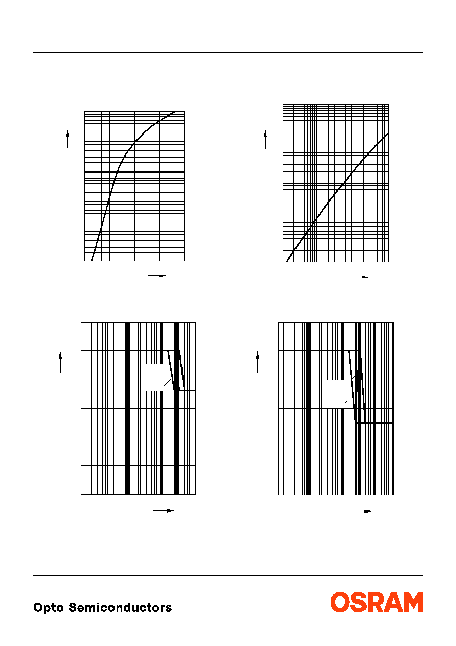
Durchlassstrom
1)
I
F
= f (V
F
)
Forward Current
T
A
= 25 ∞C
Zulassige Impulsbelastbarkeit
1)
I
F
= f (t
P
)
Permissible Pulse Handling Capability
Duty cycle D = parameter, T
A
= 25 ∞C
1)
Based on typ.(see page 2, footnote 2 for explanation)
data measured in OSRAM Opto Semiconductor's
TOPLEDÆ package.
Relative Lichtst‰rke
1)
I
V
/I
V
(50mA) = f (I
F
)
Relative Luminous Intensity
T
A
= 25 ∞C
Zulassige Impulsbelastbarkeit
1)
I
F
= f (t
P
)
Permissible Pulse Handling Capability
Duty cycle D = parameter, T
A
= 85 ∞C
OHL01382
1.3
mA
V
F
I
F
V
1.5
1.7
1.9
2.1
2.3
2.5
10
2
10
10
-3
-2
10
-1
10
0
10
1
OHL01505
F
I
0
0.02
0.04
0.06
0.08
0.1
0.12
A
p
t
-5
10
-4
10
-3
10
-2
10
-1
10
0
10
1
10
2
10
0.005
0.05
0.5
s
I
OHL00437
F
-1
10
V (50 mA)
I
10
-3
-2
-1
0
1
10
10
10
10
10
0
10
1
10
2
5
5
5
5
5
mA
I
V
OHL01506
F
I
0
0.02
0.04
0.06
0.08
0.10
0.12
A
p
t
-5
10
-4
10
-3
10
-2
10
-1
10
0
10
1
10
2
10
0.005
0.05
0.5
s