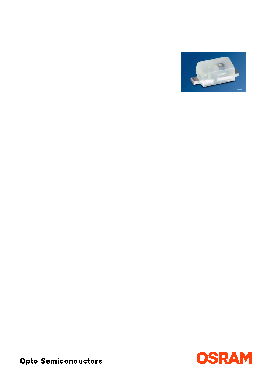
LA L89B
SmartLED
TM
Enhanced Optical Power LED (HOP2000)
Vorl‰ufige Daten / Preliminary Data
2003-05-22
1
Besondere Merkmale
∑ Geh‰usetyp: SMT Geh‰use SCD 80
∑ Besonderheit des Bauteils: kleinste Bauform
1,7 x 0,8 x 0,65 mm (LxBxH). Die SmartLED
TM
kann jede CHIPLED 0603 ersetzen. Die
SmartLED erlaubt mehr Strom bei gleicher
Chiptechnologie und Umgebungstemperatur.
Daher ist die SmartLED heller als jede
vergleichbare CHIPLED 0603.
∑ Wellenl‰nge: 617 nm
∑ Abstrahlwinkel: 160∞
∑ Technologie: InGaAlP
∑ optischer Wirkungsgrad: 19 lm/W
∑ Gruppierungsparameter: Lichtst‰rke
∑ Verarbeitungsmethode: f¸r alle
SMT-Best¸cktechniken geeignet
∑ Lˆtmethode: IR Reflow Lˆten und
Wellenlˆten (TTW)
∑ Vorbehandlung: nach JEDEC Level 2
∑ Gurtung: 8 mm Gurt mit 5000/Rolle bzw.
10000/Rolle, ¯180 mm
∑ ESD-Festigkeit: ESD-sicher bis 2 kV nach
EOS/ESD-5.1-1993
Anwendungen
∑ Informationsanzeigen im Auþenbereich
∑ Flache Hinterleuchtung (LCD, Mobile Phone,
Schalter, Display)
∑ Signal- und Symbolleuchten
∑ Ultraflache Leuchtenkonzepte unter Einsatz
geeigneter Linsensysteme f¸r den Automobil-
und Allgemeinbeleuchtungsbereiche
Features
∑ package: SMT package SCD 80
∑ feature of the device: smallest
package 1.7 x 0.8 x 0.65 mm (LxWxH). The
SmartLED
TM
can replace each CHIPLED 0603.
The SmartLED allows a higher current to drive
at the same chip technology and ambient
temperature. Therefore the SmartLED is a
superior package and is much brighter as each
comparable CHIPLED 0603.
∑ wavelength: 617 nm
∑ viewing angle: 160∞
∑ technology: InGaAlP
∑ optical efficiency: 19 lm/W
∑ grouping parameter: luminous intensity
∑ assembly methods: suitable for all
SMT assembly methods
∑ soldering methods: IR reflow soldering and
TTW soldering
∑ preconditioning: acc. to JEDEC Level 2
∑ taping: 8 mm tape with 5000/reel resp.
10000/reel, ¯180 mm
∑ ESD-withstand voltage: up to 2 kV acc. to
EOS/ESD-5.1-1993
Applications
∑ outdoor displays
∑ flat backlighting (LCD, cellular phones,
switches, displays)
∑ signal and symbol luminaire
∑ Ultra-thin lamps using special optics for
automotive and general lighting applications
2003-05-22
2
LA L89B
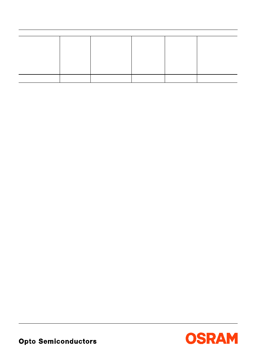
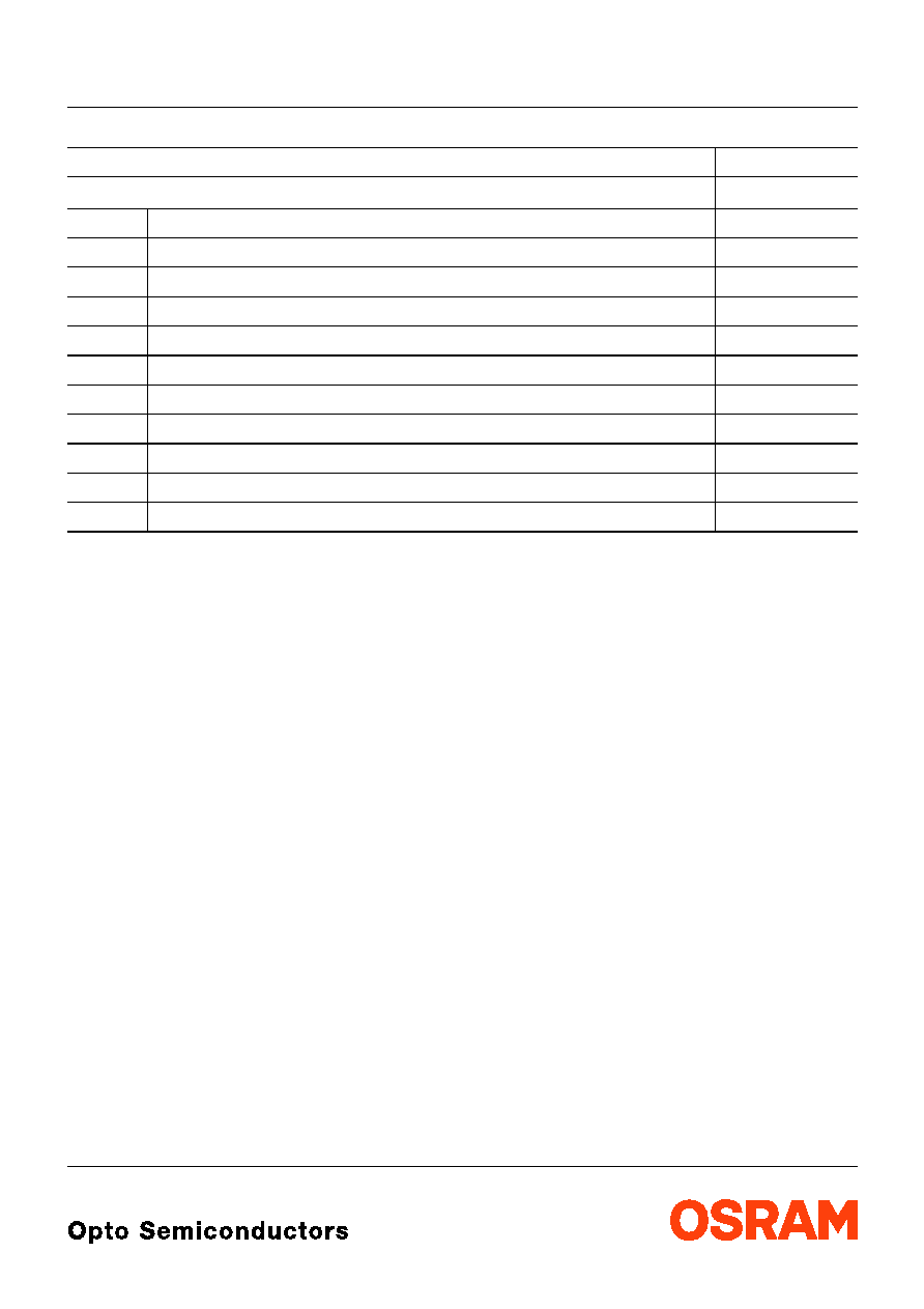
Anm.: -24 gesamter Farbbereich, Lieferung in Einzelgruppen (siehe Seite 5)
Die Standardlieferform von Serientypen beinhaltet eine Familiengruppe, die aus 4 Halbgruppen
besteht. Einzelne Halbgruppen sind nicht erh‰ltlich.
In einer Verpackungseinheit / Gurt ist immer nur eine Halbgruppe enthalten.
Dimmverh‰ltnis im Gleichstrom-Betrieb max. 5:1
Note: -24 Total color tolerance range, delivery in single groups (please see page 5)
The standard shipping format for serial types includes a family group of 4 individual groups.
Individual half groups are not available.
No packing unit / tape ever contains more than one luminous intensity half group.
Dimming range for direct current mode max. 5:1
Typ
Type
Emissions-
farbe
Color of
Emission
Geh‰usefarbe
Color of
Package
Lichtst‰rke
Luminous
Intensity
I
F
= 30 mA
I
V
(mcd)
Lichtstrom
Luminous
Flux
I
F
= 30 mA
V
(mlm)
Bestellnummer
Ordering Code
LA L89B-S1T2-24 amber
colorless diffused
180 ... 450
1200 (typ.)
Q65110A0570
LA L89B
2003-05-22
3
Grenzwerte
Maximum Ratings
Bezeichnung
Parameter
Symbol
Symbol
Wert
Value
Einheit
Unit
Betriebstemperatur
Operating temperature range
T
op
≠ 40 ... + 100
∞C
Lagertemperatur
Storage temperature range
T
stg
≠ 40 ... + 100
∞C
Sperrschichttemperatur
Junction temperature
T
j
+ 110
∞C
Durchlassstrom
Forward current
I
F
60
mA
Stoþtrom
Surge current
t
=
10
µ
s,
D
= 0.1
I
FM
0.1
A
Sperrspannung
1)
Reverse voltage
V
R
12
V
Leistungsaufnahme
Power consumption
P
tot
110
mW
W‰rmewiderstand
Thermal resistance
Sperrschicht/Umgebung
Junction/ambient
Sperrschicht/Lˆtpad
Junction/solder point
Montage auf PC-Board FR 4 (Padgrˆþe
5 mm
2
)
mounted on PC board FR 4 (pad size
5 mm
2
)
R
th JA
R
th JS
500
290
K/W
K/W
1)
f¸r kurzzeitigen Betrieb geeignet / suitable for short term application
2003-05-22
4
LA L89B
Kennwerte (
T
A
= 25 ∞C)
Characteristics
Bezeichnung
Parameter
Symbol
Symbol
Wert
Value
Einheit
Unit
Wellenl‰nge des emittierten Lichtes
(typ.)
Wavelength at peak emission
I
F
= 30 mA
peak
624
nm
Dominantwellenl‰nge
1)
(typ.)
Dominant wavelength
I
F
= 30 mA
dom
617
≠5/+7
nm
Spektrale Bandbreite bei 50 %
I
rel max
(typ.)
Spectral bandwidth at 50 %
I
rel max
I
F
= 30 mA
18
nm
Abstrahlwinkel bei 50 %
I
V
(Vollwinkel)
(typ.)
Viewing angle at 50 %
I
V
2
160
Grad
deg.
Durchlassspannung
2)
(min.)
Forward voltage
(typ.)
I
F
= 30 mA
(max.)
V
F
V
F
V
F
1.8
2.1
2.4
V
V
V
Sperrstrom
(typ.)
Reverse current
(max.)
V
R
= 12 V
I
R
I
R
0.01
10
µ
A
µ
A
Temperaturkoeffizient von
peak
(typ.)
Temperature coefficient of
peak
I
F
= 30 mA; ≠10∞C
T
100∞C
TC
peak
0.15
nm/K
Temperaturkoeffizient von
dom
(typ.)
Temperature coefficient of
dom
I
F
= 30 mA; ≠10∞C
T
100∞C
TC
dom
0.07
nm/K
Temperaturkoeffizient von
V
F
(typ.)
Temperature coefficient of
V
F
I
F
= 30 mA; ≠10∞C
T
100∞C
TC
V
≠ 3.7
mV/K
Optischer Wirkungsgrad
(typ.)
Optical efficiency
I
F
= 30 mA
opt
19
lm/W
1)
Wellenl‰ngengruppen werden mit einer Stromeinpr‰gedauer von 25 ms und einer Genauigkeit von ±1 nm ermittelt.
Wavelength groups are tested at a current pulse duration of 25 ms and a tolerance of ±1 nm.
2)
Durchlassspannungsgruppen werden mit einer Stromeinpr‰gedauer von 1 ms und einer Genauigkeit von ±0,05 V
ermittelt.
Forward voltage groups are tested at a current pulse duration of 1 ms and a tolerance of ±0.05 V.
LA L89B
2003-05-22
5
Helligkeitswerte werden mit einer Stromeinpr‰gedauer von 25 ms und einer Genauigkeit von
±
11% ermittelt.
Luminous intensity is tested at a current pulse duration of 25 ms and a tolerance of
±
11%.
1)
Wellenl‰ngengruppen
Wavelength groups
Gruppe
Group
amber
Einheit
Unit
min.
max.
2
612
616
nm
3
616
620
nm
4
620
624
nm
Helligkeits-Gruppierungsschema
Luminous Intensity Groups
Lichtgruppe
Luminous Intensity Group
Lichtst‰rke
Luminous Intensity
I
V
(mcd)
Lichtstrom
Luminous Flux
V
(mlm)
S1
S2
T1
T2
180.0 ...224.0
224.0 ...280.0
280.0 ...355.0
355.0 ...450.0
800 (typ.)
1000 (typ.)
1250 (typ.)
1600 (typ.)
Gruppenbezeichnung auf Etikett
Group Name on Label
Beispiel: S2-4
Example: S2-4
Lichtgruppe
Luminous Intensity Group
Halbgruppe
Half Group
Wellenl‰nge
Wavelength
S
2
4
2003-05-22
6
LA L89B
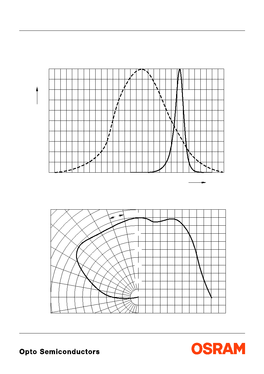
Relative spektrale Emission
I
rel
=
f
(
),
T
A
= 25 ∞C,
I
F
= 30 mA
Relative Spectral Emission
V(
) = spektrale Augenempfindlichkeit
Standard eye response curve
Abstrahlcharakteristik
I
rel
=
f
(
)
Radiation Characteristic
OHL00436
400
0
20
40
60
80
100
450
500
550
600
650
700
nm
%
I
rel
V
amber
OHL01440
0∞
20∞
40∞
60∞
80∞
100∞
120∞
0.4
0.6
0.8
1.0
100∞
90∞
80∞
70∞
60∞
50∞
0∞
10∞
20∞
30∞
40∞
0
0.2
0.4
0.6
0.8
1.0
LA L89B
2003-05-22
7
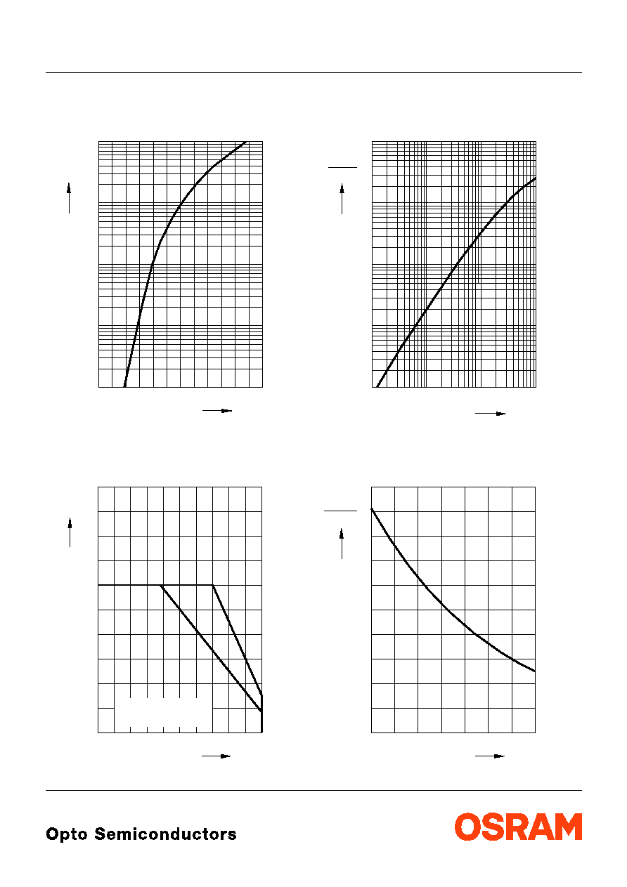
Durchlassstrom
I
F
=
f
(
V
F
)
Forward Current
T
A
= 25 ∞C
Maximal zul‰ssiger Durchlassstrom
I
F
=
f
(
T
A
)
Max. Permissible Forward Current
Relative Lichtst‰rke
I
V
/
I
V(30 mA)
=
f
(
I
F
)
Relative Luminous Intensity
T
A
= 25 ∞C
Relative Lichtst‰rke
I
V
/
I
V(25 ∞C)
=
f
(
T
A
)
Relative Luminous Intensity
I
F
= 30 mA
OHL00590
10
-2
10
-1
10
0
10
1
F
V
10
2
F
I
mA
2.3
1.3
1.5
1.7
1.9
2.1
V 2.5
OHL00666
0
0
20
40
60
80 ∞C 100
mA
F
I
T
temp. solder point
temp. ambient
T
T
S
A
T
T
A
S
20
40
60
80
100
10
30
50
70
V
V (30 mA)
10
-1
0
10
10
1
2
10
mA
10
-3
5
OHL00874
F
I
5
-2
10
5
-1
10
0
10
1
10
I
I
5
5
OHL00740
0
-40
∞C
T
(25 ∞C)
I
V
I
V
0.2
0.4
0.6
0.8
1.0
1.2
1.4
1.6
2.0
-20
0
20
40
60
100
LA L89B
2003-05-22
8
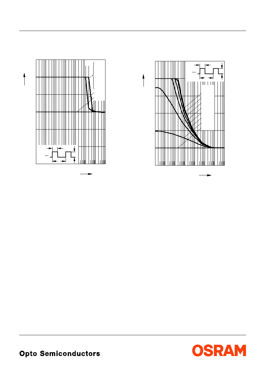
Zul‰ssige Impulsbelastbarkeit
I
F
=
f
(
t
p
)
Permissible Pulse Handling Capability
Duty cycle
D
= parameter,
T
A
= 25 ∞C
Zul‰ssige Impulsbelastbarkeit
I
F
=
f
(
t
p
)
Permissible Pulse Handling Capability
Duty cycle
D
= parameter,
T
A
= 85 ∞C
OHL00673
10
-5
p
t
F
I
10
-4
10
-3
10
-2
10
-1
10
0
10
1
0
A
2
10
s
0.02
0.04
0.06
0.08
0.12
t
P
=
D
T
T
P
t
I
F
0.01
0.05
0.2
0.1
0.005
0.02
0.5
D
=
1
OHL00674
10
-5
p
t
F
I
10
-4
10
-3
10
-2
10
-1
10
0
10
1
0
A
2
10
s
0.01
0.05
0.2
0.1
0.005
0.02
0.5
D
=
0.02
0.04
0.06
0.08
0.12
1
t
P
=
D
T
T
P
t
I
F
LA L89B
2003-05-22
9
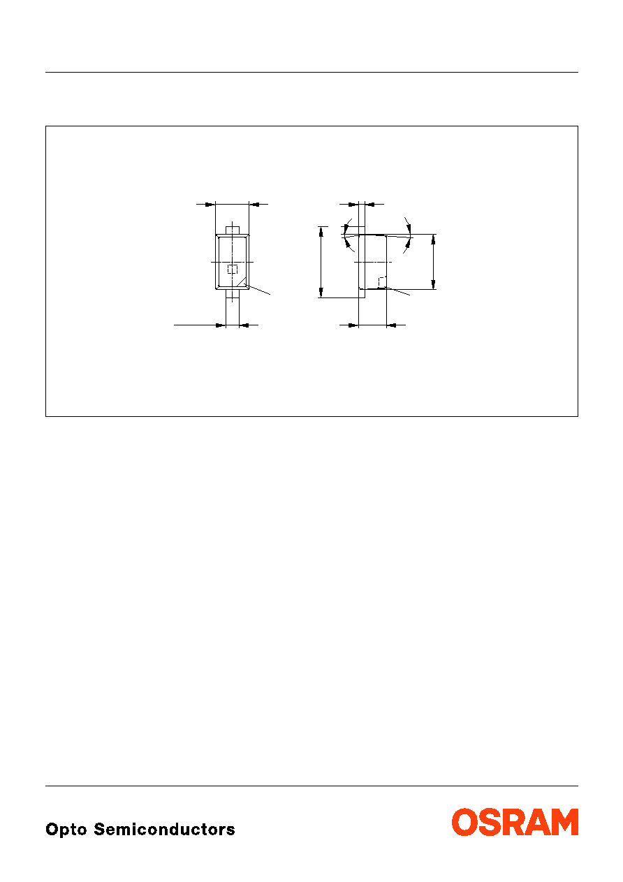
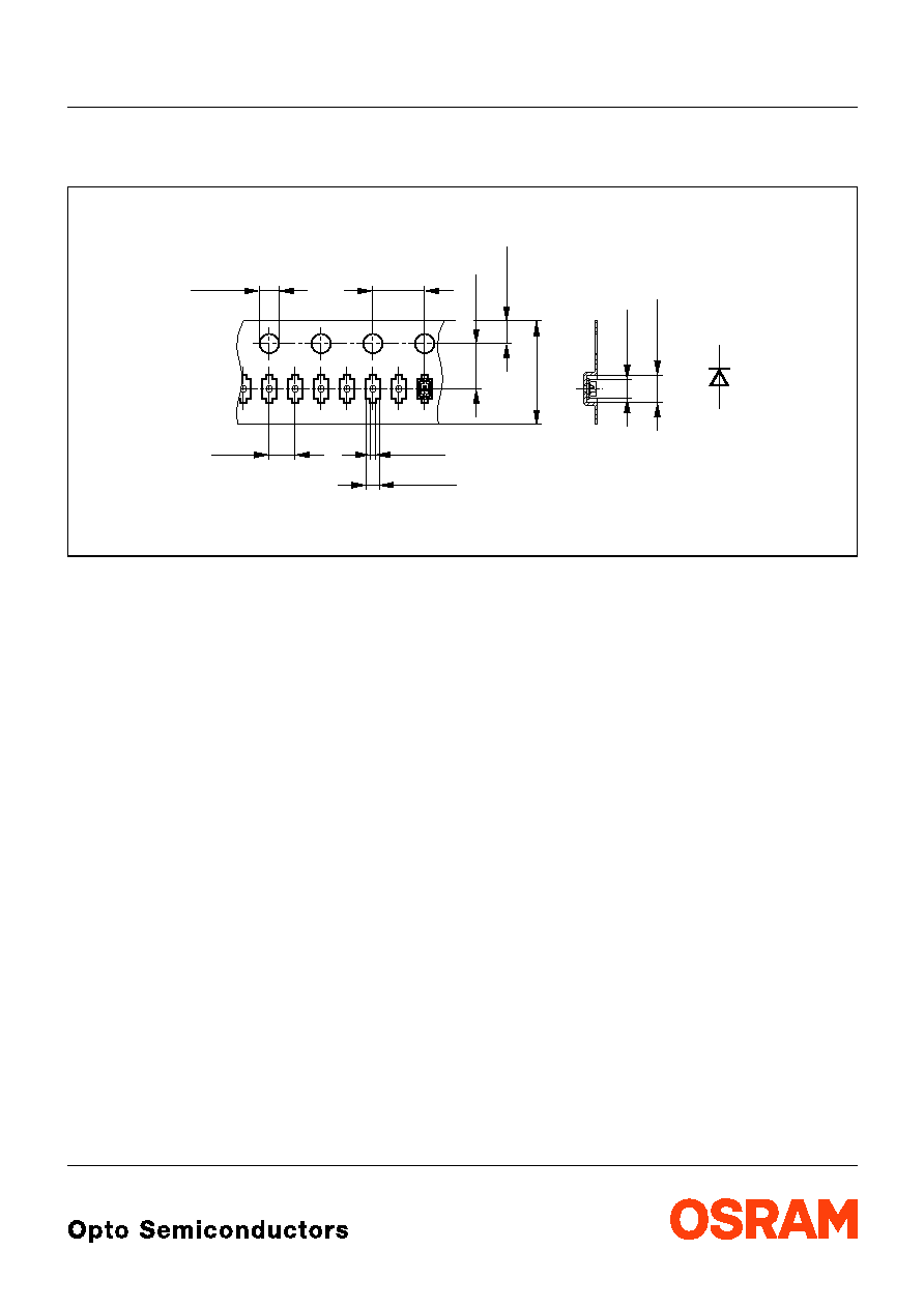
Maþzeichnung
Package Outlines
Maþe werden wie folgt angegeben: mm (inch) / Dimensions are specified as follows: mm (inch).
Gewicht / Approx. weight: 1,4 mg
GPLY6057
0.8 (0.031)
±0.1 (0.004)
Cathode
0.3 (0.012)
+0.05 (0.002)
-0.03 (0.001)
0.125 (0.005)
1.7 (0.067)
±0.1 (0.004)
7
∞
max
+0.02 (0.001)
-0.05 (0.002)
0.65 (0.026)
5
∞
1.3 (0.051)
±0.1 (0.004)
marking
marking
Cathode
2003-05-22
10
LA L89B
Lˆtbedingungen
Vorbehandlung nach JEDEC Level 2
Soldering Conditions Preconditioning acc. to JEDEC Level 2
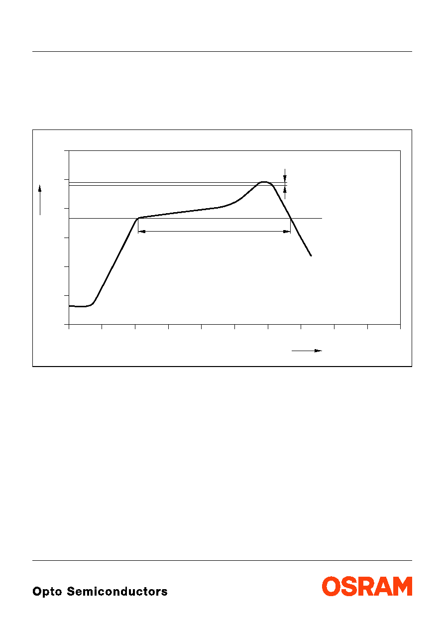
IR-Reflow Lˆtprofil
(nach IPC 9501)
IR Reflow Soldering Profile
(acc. to IPC 9501)
OHLY0597
0
0
50
100
150
200
250
50
100
150
200
250
300
T
t
∞C
s
240-245 ∞C
10-40 s
183 ∞C
120 to 180 s
Defined for Preconditioning: up to 6 K/s
Ramp-down rate up to 6 K/s
Ramp-up rate up to 6 K/s
Defined for Preconditioning: 2-3 K/s
LA L89B
2003-05-22
11
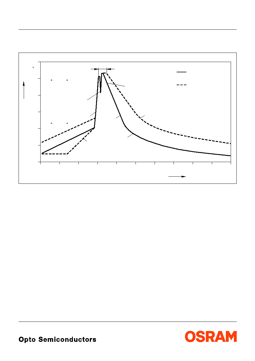
Wellenlˆten (TTW)
(nach CECC 00802)
TTW Soldering
(acc. to CECC 00802)
OHLY0598
0
0
50
100
150
200
250
50
100
150
200
250
300
T
t
C
s
235 C
10 s
C
... 260
1. Welle
1. wave
2. Welle
2. wave
5 K/s
2 K/s
ca 200 K/s
C
C
... 130
100
2 K/s
Zwangsk¸hlung
forced cooling
Normalkurve
standard curve
Grenzkurven
limit curves
2003-05-22
12
LA L89B
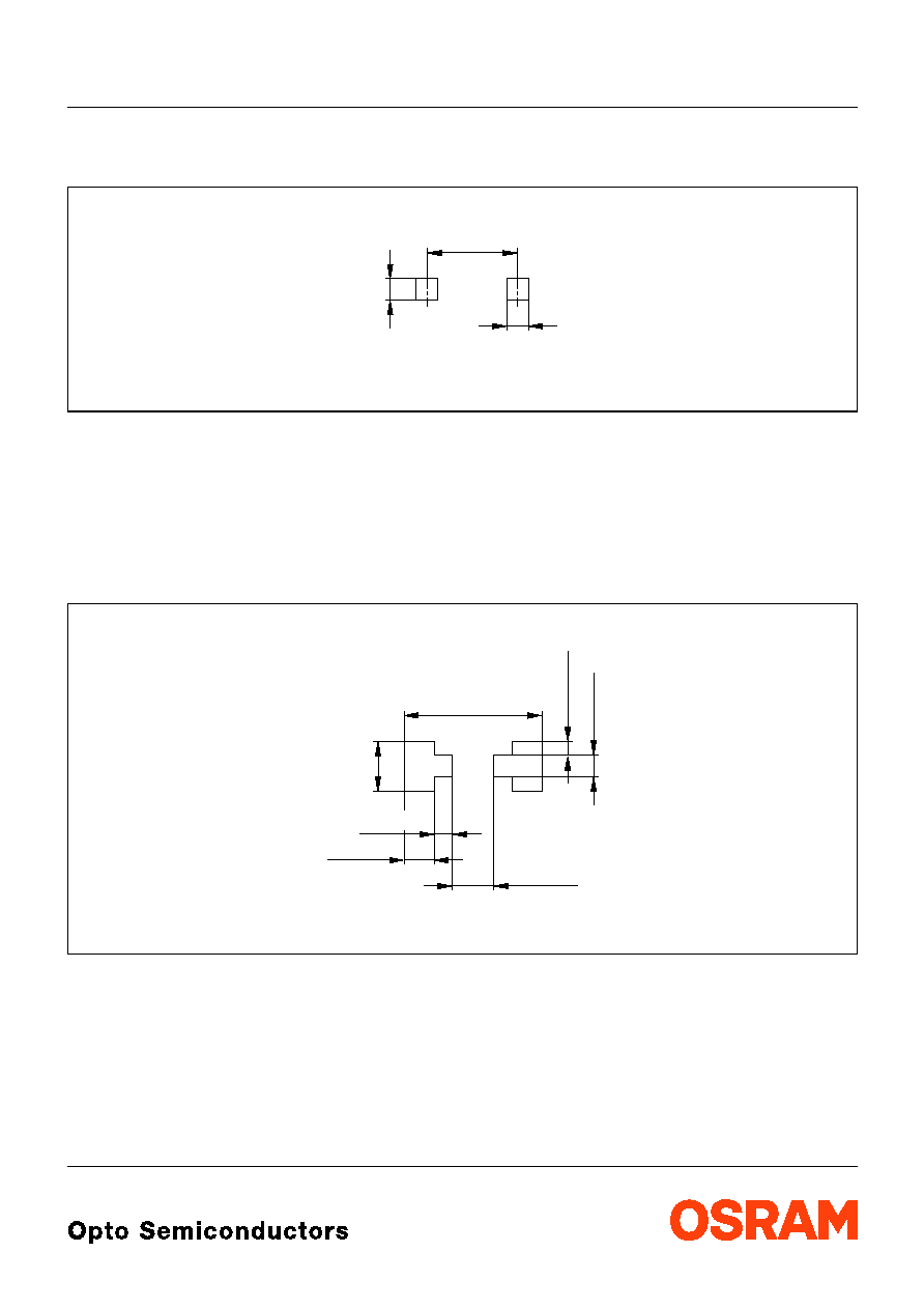
Empfohlenes Lˆtpaddesign
IR Reflow Lˆten
Recommended Solder Pad
IR Reflow Soldering
Maþe werden wie folgt angegeben: mm (inch) / Dimensions are specified as follows: mm (inch).
Geh‰use h‰lt TTW-Lˆthitze aus / Package able to withstand TTW-soldering heat
Empfohlenes Lˆtpaddesign verwendbar f¸r SmartLED
TM
und Chipled - Bauform 0603
IR Reflow Lˆten
Recommended Solder Pad useable for SmartLED
TM
and Chipled - Package 0603
IR Reflow Soldering
Maþe werden wie folgt angegeben: mm (inch) / Dimensions are specified as follows: mm (inch).
Empfohlene Lˆtpastendicke: 120 µm/ recommended thickness of solder paste: 120 µm
Geh‰use f¸r Wellenlˆten (TTW) geeignet / Package suitable for TTW-soldering
OHPY1301
1.45 (0.057)
0.35 (0.014)
0.35 (0.014)
OHPY0203
2.25 (0.089)
0.65 (0.026)
0.3 (0.012)
0.5 (0.020)
0.8 (0.031)
0.35 (0.014)
0.225 (0.009)
LA L89B
2003-05-22
13
Gurtung / Polarit‰t und Lage
Method of Taping / Polarity and Orientation
Maþe werden wie folgt angegeben: mm (inch) / Dimensions are specified as follows: mm (inch).
Verpackungseinheit:
8 mm Gurt mit 5000/Rolle, ¯180 mm
8 mm Gurt mit 10000/Rolle, ¯180 mm (auf Anfrage)
Packing unit:
8 mm tape with 5,00/reel, ¯180 mm
8 mm tape with 10000/reel, ¯180 mm (on request)
OHAY1350
1.5 (0.059)
4 (0.157)
2 (0.079)
0.4 (0.016)
0.93 (0.037)
3.5 (0.138)
1.75 (0.069)
8 (0.315)
1.4 (0.055)
2.04 (0.080)
A
C
2003-05-22
14
LA L89B
Published by OSRAM Opto Semiconductors GmbH
Wernerwerkstrasse 2, D-93049 Regensburg
© All Rights Reserved.
Attention please!
The information describes the type of component and shall not be considered as assured characteristics.
All typical data and graphs are basing on representative samples, but don't represent the production range. If requested,
e.g. because of technical improvements, these typ. data will be changed without any further notice.
Terms of delivery and rights to change design reserved. Due to technical requirements components may contain
dangerous substances. For information on the types in question please contact our Sales Organization.
If printed or downloaded, please find the latest version in the Internet.
Packing
Please use the recycling operators known to you. We can also help you ≠ get in touch with your nearest sales office.
By agreement we will take packing material back, if it is sorted. You must bear the costs of transport. For packing
material that is returned to us unsorted or which we are not obliged to accept, we shall have to invoice you for any costs
incurred.
Components used in life-support devices or systems must be expressly authorized for such purpose! Critical
components
1
may only be used in life-support devices or systems
2
with the express written approval of OSRAM OS.
1
A critical component is a component used in a life-support device or system whose failure can reasonably be expected
to cause the failure of that life-support device or system, or to affect its safety or the effectiveness of that device or
system.
2
Life support devices or systems are intended (a) to be implanted in the human body, or (b) to support and/or maintain
and sustain human life. If they fail, it is reasonable to assume that the health of the user may be endangered.
Revision History: 2003-05-22
Date of change
Previous Version:
2002-12-10
Page
Subjects (major changes since last revision)
1 & 4
change of optical efficiency from 24 to 19 lm/W
1
increase of "feature of device" and "applications"
3
pad size from 16 mm
2
to 5 mm
2
7
change of diagram rel. lum. intensity (T
A
) from OHL01640 to OHL00740
2 & 5
insert of wavelength groups
2002-07-19
14
annotations
2002-07-23
3, 4
value (reverse voltage from 5 V to 12 V)
2002-09-18
2
ordering code
2002-10-25
1, 13
tape with 5000/reel and 10000/reel instead of 10000
2002-12-10
7
diagram forward current OHL01382 replaced by OHL00590
2003-02-12