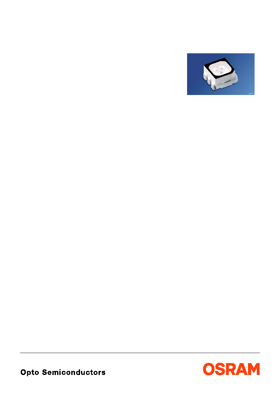
LATB G66B
6-lead MULTILED
Æ
Enhanced optical Power LED (HOP2000 / ATON
Æ
)
Vorl‰ufige Daten / Preliminary Data
2003-11-17
1
Besondere Merkmale
∑
Geh‰usetyp: weiþes P-LCC-6 Geh‰use,
Kontrasterhˆhung durch schwarze Oberfl‰che
(RGB-Displays) und diffuses Harz
∑
Besonderheit des Bauteils: additive
Farbmischung durch unabh‰ngige Ansteuerung
aller Chips
∑
Wellenl‰nge: 617 nm (amber),
528 nm (true green), 470 nm (blau)
∑
Abstrahlwinkel: Lambertscher Strahler (120∞)
∑
Technologie: InGaAlP (amber),
InGaN (true green, blau)
∑
optischer Wirkungsgrad: 24 lm/W (amber),
13 lm/W (true green), 3 lm/W (blau)
∑
Gruppierungsparameter: Lichtst‰rke,
Wellenl‰nge
∑
Verarbeitungsmethode: f¸r alle
SMT-Best¸cktechniken geeignet
∑
Lˆtmethode: IR Reflow Lˆten
∑
Vorbehandlung: nach JEDEC Level 2
∑
Gurtung: 12 mm Gurt mit 1000/Rolle, ¯180 mm
oder 4000/Rolle, ¯330 mm
∑
ESD-Festigkeit: ESD-sicher bis 2 kV nach
JESD22-A114-B
Anwendungen
∑
Anzeigen im Innen- und Auþenbereich
(z.B. im Verkehrsbereich; Laufschriftanzeigen)
∑
Getrennte Anteuerung der Leuchtdiodenchips zur
Darstellung verschiedener Farben inclusive weiþ
∑
Vollfarbdisplays bzw. RGB-Displays
∑
Hinterleuchtung (LCD, Schalter, Tasten,
Werbebeleuchtung, Allgemeinbeleuchtung)
∑
Einkopplung in Lichtleiter
Features
∑
package: white P-LCC-6 package, higher
contrast by a black surface (RGB-Displays) and
diffused resin
∑
feature of the device: additive mixture of color
stimuli by independent driving of each chip
∑
wavelength: 617 nm (amber),
528 nm (true green), 470 nm (blue)
∑
viewing angle: Lambertian Emitter (120∞)
∑
technology: InGaAlP (amber),
InGaN (true green, blue)
∑
optical efficiency: 24 lm/W (amber),
13 lm/W (true green), 3 lm/W (blue)
∑
grouping parameter: luminous intensity,
wavelength
∑
assembly methods: suitable for all
SMT assembly methods
∑
soldering methods: IR reflow soldering
∑
preconditioning: acc. to JEDEC Level 2
∑
taping: 12 mm tape with 1000/reel, ¯180 mm
or 4000/reel, ¯330 mm
∑
ESD-withstand voltage: up to 2 kV acc. to
JESD22-A114-B
Applications
∑
indoor and outdoor displays (e.g. displays for
traffic; light writing displays)
∑
LED chips can be controlled seperately to display
various colors including white
∑
full color displays, RGB-Displays
∑
backlighting (LCD, switches, keys, illuminated
advertising, general lighting)
∑
coupling into light guides

2003-11-17
2
LATB G66B
Anm.: -78 gesamter Farbbereich, Lieferung in Einzelgruppen (siehe Seite 5)
Die
Standardlieferform
von
Serientypen
beinhaltet
eine
Familiengruppe.
Einzelne
Helligkeitsgruppen sind nicht bestellbar.
In einer Verpackungseinheit / Gurt ist immer nur eine Helligkeitsgruppe pro Farbe enthalten.
Dimmverh‰ltnis im Gleichstrom-Betrieb max. 5:1 f¸r amber
Note: -78 Total color tolerance range, delivery in single groups (please see page 5)
The standard shipping format for serial types includes a family group. Individual luminous
intensity groups cannot be ordered.
No packing unit / tape ever contains more than one luminous intensity group per color.
Dimming range for direct current mode max. 5:1 for amber
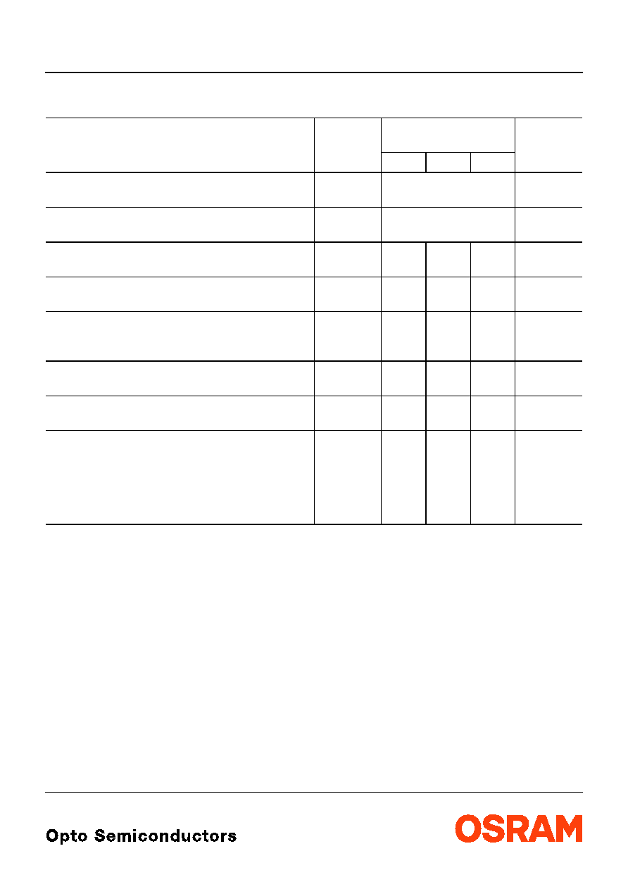
Typ
Type
Emissions-
farbe
Color of Emission
Lichtst‰rke
Luminous Intensity
I
F
= 20 mA
I
V
(mcd)
amber
true green
blue
LATB G66B
amber
true green
blue
180 ... 450
450 ...1120
71 ...180
Bestell - Information
Ordering Information
Typ
Type
Bestellnummer
Ordering Code
LATB G66B-ST-1+TU-35+QR-78
LATB G66B-ST-1+UV-35+QR-78
Q65110A0728
Q65110A1539
LATB G66B
2003-11-17
3
Grenzwerte
Maximum Ratings
Bezeichnung
Parameter
Symbol
Symbol
Werte
Values
Einheit
Unit
LA
LT
LB
Betriebstemperatur
Operating temperature range
T
op
≠ 40 ... + 100
∞C
Lagertemperatur
Storage temperature range
T
stg
≠ 40 ... + 100
∞C
Sperrschichttemperatur
Junction temperature
T
j
+ 125
+ 125
+ 110
∞C
Durchlassstrom
Forward current (
T
A
=25∞C)
I
F
70
30
30
mA
Stoþstrom
Surge current
t
p
= 10
µ
s,
D
= 0.005,
T
A
=25∞C
I
FM
100
250
200
mA
Sperrspannung
1)
Reverse voltage (
T
A
=25∞C)
V
R
12
5
5
V
Leistungsaufnahme
Power consumption (
T
A
=25∞C)
P
tot
180
140
140
mW
W‰rmewiderstand
Thermal resistance
Sperrschicht/Umgebung
2)
1 chip on
Junction/ambient
2)
3 chips on
Sperrschicht/Lˆtpad
1 chip on
Junction/solder point
3 chips on
R
th JA
R
th JA
R
th JS
R
th JS
350
560
200
200
400
640
230
230
400
640
230
230
K/W
K/W
K/W
K/W
1)
f¸r kurzzeitigen Betrieb geeignet / suitable for short term application
2)
Montage auf PC-Board FR 4 (Padgrˆþe
16 mm
2
)
mounted on PC board FR 4 (pad size
16 mm
2
)

2003-11-17
4
LATB G66B
Kennwerte (
T
A
= 25 ∞C)
Characteristics
Bezeichnung
Parameter
Symbol
Symbol
Werte
Values
Einheit
Unit
LA
LT
LB
Wellenl‰nge des emittierten Lichtes
(typ.)
Wavelength at peak emission
I
F
= 20 mA
peak
624
523
465
nm
Dominantwellenl‰nge
1)
Dominant wavelength
I
F
= 20 mA
dom
617
≠2/+7
528
± 9
470
± 6
nm
Spektrale Bandbreite bei 50 %
I
rel max
(typ.)
Spectral bandwidth at 50 %
I
rel max
I
F
= 20 mA
18
33
25
nm
Abstrahlwinkel bei 50 %
I
V
(Vollwinkel)
(typ.)
Viewing angle at 50 %
I
V
2
120
120
120
Grad
deg.
Durchlassspannung
2)
(min.)
Forward voltage
(typ.)
I
F
= 20 mA
(max.)
V
F
V
F
V
F
2.0
2.4
3.5
4.1
3.6
4.1
V
V
V
Sperrstrom
(typ.)
Reverse current
(max.)
V
R
= 5 V (blue / true green); 12 V (amber)
I
R
I
R
0.01
10
0.01
10
0.01
10
µ
A
µ
A
Temperaturkoeffizient von
peak
(typ.)
Temperature coefficient of
peak
I
F
= 20 mA; ≠10∞C
T
100∞C
TC
peak
0.15
0.04
0.05
nm/K
Temperaturkoeffizient von
dom
(typ.)
Temperature coefficient of
dom
I
F
= 20 mA; ≠10∞C
T
100∞C
TC
dom
0.07
0.03
0.04
nm/K
Temperaturkoeffizient von
V
F
(typ.)
Temperature coefficient of
V
F
I
F
= 20 mA; ≠10∞C
T
100∞C
TC
V
≠ 3.7
≠ 3.6
≠ 3.1
mV/K
Optischer Wirkungsgrad
(typ.)
Optical efficiency
I
F
= 20 mA
opt
24
13
3
lm/W
1)
Wellenl‰ngen werden mit einer Stromeinpr‰gedauer von 25 ms und einer Genauigkeit von ± 1 nm ermittelt.
Wavelengths are tested at a current pulse duration of 25 ms and a tolerance of ± 1 nm.
2)
Durchlassspannungen werden mit einer Stromeinpr‰gedauer von 1 ms und einer Genauigkeit von ± 0,1 V ermittelt.
Forward voltages are tested at a current pulse duration of 1 ms and a tolerance of ± 0.1 V.

LATB G66B
2003-11-17
5
Helligkeitswerte werden mit einer Stromeinpr‰gedauer von 25 ms und einer Genauigkeit von ±11 % ermittelt.
Luminous intensity is tested at a current pulse duration of 25 ms and a tolerance of ±11 %.
1)
Wellenl‰ngengruppen f¸r Dominantwellenl‰nge
Wavelength groups for dominant wavelength
Gruppe
Group
true green
Einheit
Unit
Gruppe
Group
blue
Einheit
Unit
min.
max.
min.
max.
3
518.5
526.5
nm
7
463.5
471.5
nm
4
523.5
531.5
nm
8
468.5
476.5
nm
5
528.5
536.5
nm
Lichtgruppe
Luminous
Intensity
Group
Lichtst‰rke
Luminous
Intensity
I
V
(mcd)
Lichtstrom
Luminous
Flux
V
(mlm)
Lichtst‰rke
Luminous
Intensity
I
V
(mcd)
Lichtstrom
Luminous
Flux
V
(mlm)
Lichtst‰rke
Luminous
Intensity
I
V
(mcd)
Lichtstrom
Luminous
Flux
V
(mlm)
amber
true green
blue
S+T+Q
S+T+R
S+U+Q
S+U+R
S+V+Q
S+V+R
T+T+Q
T+T+R
T+U+Q
T+U+R
T+V+Q
T+V+R
180 ... 280
180 ... 280
180 ... 280
180 ... 280
180 ... 280
180 ... 280
280 ... 450
280 ... 450
280 ... 450
280 ... 450
280 ... 450
280 ... 450
680 (typ.)
680 (typ.)
680 (typ.)
680 (typ.)
680 (typ.)
680 (typ.)
1075 (typ.)
1075 (typ.)
1075 (typ.)
1075 (typ.)
1075 (typ.)
1075 (typ.)
280 ... 450
280 ... 450
450 ... 710
450 ... 710
710 ...1120
710 ...1120
280 ... 450
280 ... 450
450 ... 710
450 ... 710
710 ...1120
710 ...1120
1075 (typ.)
1075 (typ.)
1700 (typ.)
1700 (typ.)
2700 (typ.)
2700 (typ.)
1075 (typ.)
1075 (typ.)
1700 (typ.)
1700 (typ.)
2700 (typ.)
2700 (typ.)
71 ... 112
112 ... 180
71 ... 112
112 ... 180
71 ... 112
112 ... 180
71 ... 112
112 ... 180
71 ... 112
112 ... 180
71 ... 112
112 ... 180
270 (typ.)
430 (typ.)
270 (typ.)
430 (typ.)
270 (typ.)
430 (typ.)
270 (typ.)
430 (typ.)
270 (typ.)
430 (typ.)
270 (typ.)
430 (typ.)

2003-11-17
6
LATB G66B
Gruppenbezeichnung auf Etikett
Group Name on Label
Beispiel: T-1+U-4+R-7
Example: T-1+U-4+R-7
Lichtgruppe
Luminous
Intensity
Group
(amber)
Wellenl‰nge
(keine
Gruppierung)
Wavelength
(no grouping)
(amber)
Lichtgruppe
Luminous
Intensity
Group
(true green)
Wellenl‰nge
Wavelength
(true green)
Lichtgruppe
Luminous
Intensity
Group
(blue)
Wellenl‰nge
Wavelength
(blue)
T
1
U
4
R
7

2003-11-17
7
LATB G66B
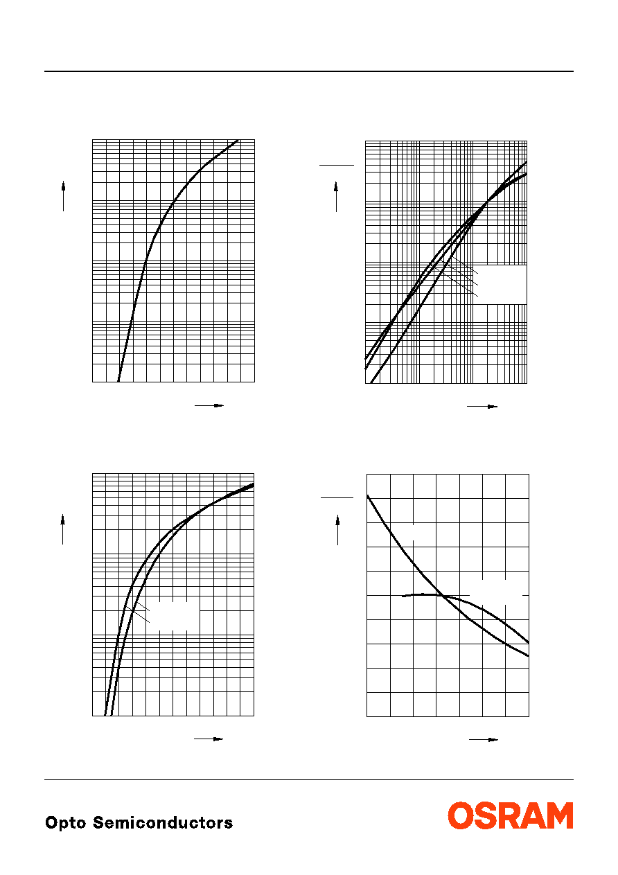
Relative spektrale Emission
I
rel
=
f
(
),
T
A
= 25 ∞C,
I
F
= 20 mA
Relative Spectral Emission
V(
) = spektrale Augenempfindlichkeit
Standard eye response curve
Abstrahlcharakteristik
I
rel
=
f
(
)
Radiation Characteristic
0
350
nm
OHL01452
I
20
40
60
80
%
100
rel
blue
400
450
500
550
600
650
700
true green
V
amber
0
0.2
0.4
1.0
0.8
0.6
1.0
0.8
0.6
0.4
0∞
10∞
20∞
40∞
30∞
OHL01660
50∞
60∞
70∞
80∞
90∞
100∞
0∞
20∞
40∞
60∞
80∞
100∞
120∞
LATB G66B
2003-11-17
8
Durchlassstrom
I
F
=
f
(
V
F
)
Forward Current
T
A
= 25 ∞C; amber
Durchlassstrom
I
F
=
f
(
V
F
)
Forward Current
T
A
= 25 ∞C
Relative Lichtst‰rke
I
V
/
I
V(20 mA)
=
f
(
I
F
)
Relative Luminous Intensity
T
A
= 25 ∞C
Relative Lichtst‰rke
I
V
/
I
V(25 ∞C)
=
f
(
T
A
)
Relative Luminous Intensity
I
F
= 20 mA
OHL00590
10
-2
10
-1
10
0
10
1
F
V
10
2
F
I
mA
2.3
1.3
1.5
1.7
1.9
2.1
V 2.5
OHL01481
I
F
3.5
2
3
2.5
5
V
4.5
4
V
F
5
mA
10
2
10
-1
5
10
0
5
10
1
true green
blue
V
V (20 mA)
10
-1
0
10
10
1
2
10
mA
OHL01473
F
I
I
I
5
5
true green
blue
1
10
-2
-3
10
10
5
-1
0
5
10
5
10
amber
OHL01477
0
-40
∞C
T
(25 ∞C)
I
V
I
V
0.2
0.4
0.6
0.8
1.0
1.2
1.4
1.6
2.0
-20
0
20
40
60
100
amber
true green,
blue

LATB G66B
2003-11-17
9
Dominante Wellenl‰nge
dom
=
f
(
I
F
)
Dominant Wavelength
LB
, T
A
= 25 ∞C
Dominante Wellenl‰nge
dom
=
f
(
I
F
)
Dominant Wavelength
LT
, T
A
= 25 ∞C
I
OHL10503
467
dom
0
mA
nm
20
40
60
80
120
468
469
470
471
472
473
474
blue
f
I
OHL00882
510
dom
0
mA
nm
20
40
60
80
120
515
520
525
530
535
540
550
f
true green

LATB G66B
2003-11-17
10
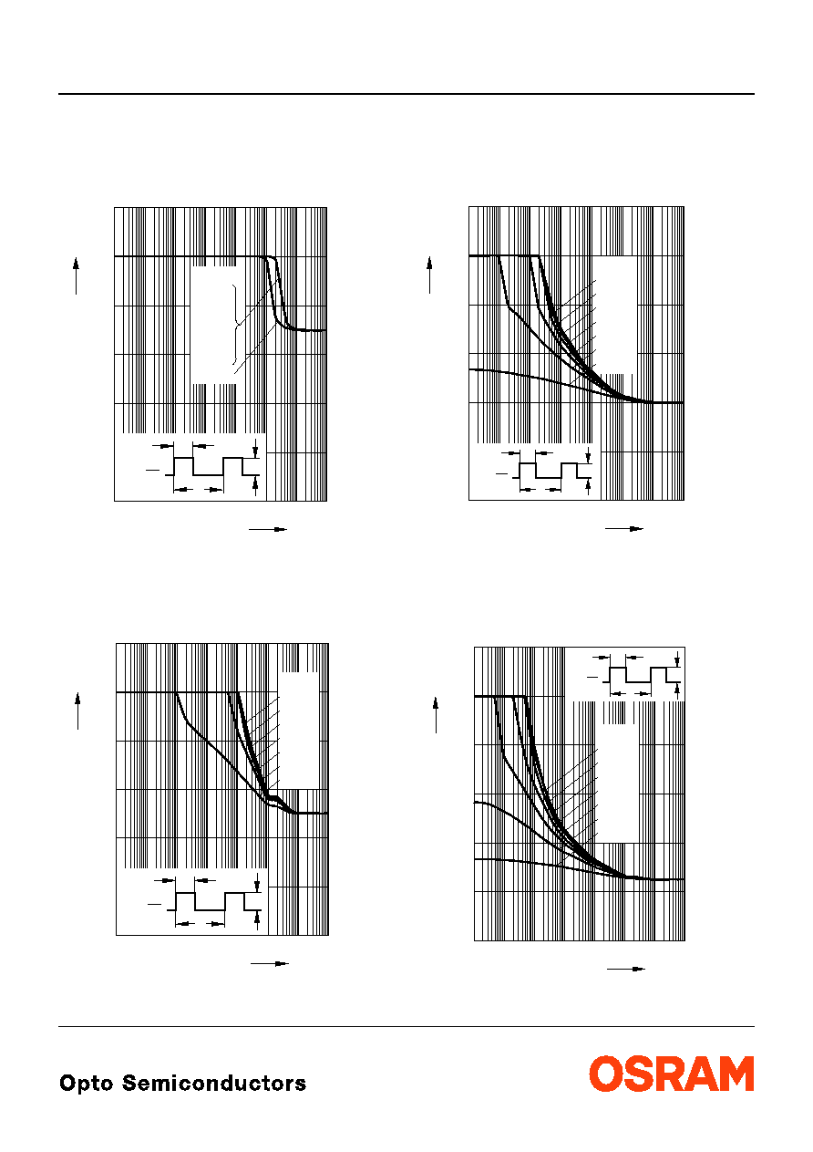
Maximal zul‰ssiger Durchlassstrom
I
F
=
f
(
T
)
Max. Permissible Forward Current
1 chip on
Maximal zul‰ssiger Durchlassstrom
I
F
=
f
(
T
)
Max. Permissible Forward Current
1 chip on
Maximal zul‰ssiger Durchlassstrom
I
F
=
f
(
T
)
Max. Permissible Forward Current
3 chips on
Maximal zul‰ssiger Durchlassstrom
I
F
=
f
(
T
)
Max. Permissible Forward Current
3 chips on
OHL00710
0
0
20
40
60
80 ∞C 100
mA
F
I
T
S
10
20
30
40
50
60
70
80
amber
blue
true green
S
T
temp. solder point
OHL00712
0
0
20
40
60
80 ∞C 100
mA
F
I
T
A
10
20
30
40
50
60
70
80
amber
blue
true green
temp. ambient
A
T
OHL00711
0
0
20
40
60
80 ∞C 100
mA
F
I
T
S
amber
blue
true green
10
20
30
40
50
60
S
T
temp. solder point
OHL00713
0
0
20
40
60
80 ∞C 100
mA
F
I
T
A
amber
blue
true green
10
20
30
40
50
60
temp. ambient
A
T
LATB G66B
2003-11-17
11
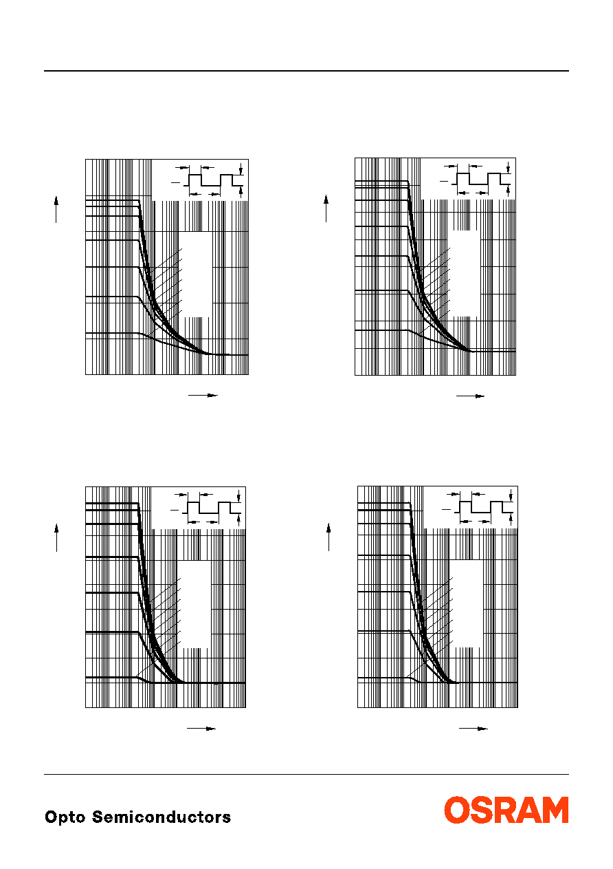
Zul‰ssige Impulsbelastbarkeit
I
F
=
f
(
t
p
)
Permissible Pulse Handling Capability
Duty cycle
D
= parameter,
T
A
= 25 ∞C
amber (1 Chip on)
Zul‰ssige Impulsbelastbarkeit
I
F
=
f
(
t
p
)
Permissible Pulse Handling Capability
Duty cycle
D
= parameter,
T
A
= 25 ∞C
amber (3 Chips on)
Zul‰ssige Impulsbelastbarkeit
I
F
=
f
(
t
p
)
Permissible Pulse Handling Capability
Duty cycle
D
= parameter,
T
A
= 85 ∞C
amber (1Chip on)
Zul‰ssige Impulsbelastbarkeit
I
F
=
f
(
t
p
)
Permissible Pulse Handling Capability
Duty cycle
D
= parameter,
T
A
= 85 ∞C
amber (3 Chips on)
OHL00728
F
I
0
p
t
-5
10
-4
10
-3
10
-2
10
-1
10
0
10
1
10
2
10
s
P
D
T
P
t
=
t
T
F
I
0.02
0.04
0.06
0.08
0.10
0.12
A
0.05
0.2
0.1
0.5
0.005
D
0.02
0.01
=
OHL00726
F
I
0
p
t
-5
10
-4
10
-3
10
-2
10
-1
10
0
10
1
10
2
10
s
P
D
T
P
t
=
t
T
F
I
0.02
0.04
0.06
0.08
0.10
0.12
A
0.05
0.5
0.2
0.1
0.01
0.02
0.005
D
=
OHL00729
F
I
0
p
t
-5
10
-4
10
-3
10
-2
10
-1
10
0
10
1
10
2
10
s
D
0.5
0.02
0.005
0.1
0.2
=
0.05
0.01
0.02
0.04
0.06
0.08
A
0.12
0.10
t
P
t
D
T
=
I
T
F
P
OHL00727
F
I
0
p
t
-5
10
-4
10
-3
10
-2
10
-1
10
0
10
1
10
2
10
s
0.02
0.04
0.06
0.08
0.10
0.12
A
0.05
0.5
0.2
0.1
0.01
0.02
0.005
D
=
t
P
t
D
T
=
I
T
F
P
LATB G66B
2003-11-17
12
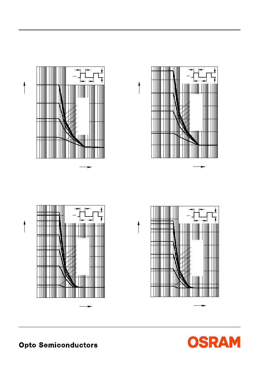
Zul‰ssige Impulsbelastbarkeit
I
F
=
f
(
t
p
)
Permissible Pulse Handling Capability
Duty cycle
D
= parameter,
T
A
= 25 ∞C
true green (1 Chip on)
Zul‰ssige Impulsbelastbarkeit
I
F
=
f
(
t
p
)
Permissible Pulse Handling Capability
Duty cycle
D
= parameter,
T
A
= 25 ∞C
true green (3 Chips on)
Zul‰ssige Impulsbelastbarkeit
I
F
=
f
(
t
p
)
Permissible Pulse Handling Capability
Duty cycle
D
= parameter,
T
A
= 85 ∞C
true green (1 Chip on)
Zul‰ssige Impulsbelastbarkeit
I
F
=
f
(
t
p
)
Permissible Pulse Handling Capability
Duty cycle
D
= parameter,
T
A
= 85 ∞C
true green (3 Chips on)
OHL00724
F
I
0
p
t
-5
10
-4
10
-3
10
-2
10
-1
10
0
10
1
10
2
10
s
D
0.5
0.02
0.005
0.1
0.2
=
0.05
0.01
0.05
0.10
0.15
0.20
A
0.30
0.25
=
D
t
P
T
T
P
t
I
F
OHL00722
F
I
0
p
t
-5
10
-4
10
-3
10
-2
10
-1
10
0
10
1
10
2
10
s
D
0.5
0.02
0.005
0.1
0.2
=
0.05
0.01
A
0.02
0.04
0.06
0.08
0.10
0.12
0.14
0.18
=
D
t
P
T
T
P
t
I
F
OHL00725
F
I
0
p
t
-5
10
-4
10
-3
10
-2
10
-1
10
0
10
1
10
2
10
s
D
0.5
0.02
0.005
0.1
0.2
=
0.05
0.01
0.02
0.04
0.06
0.08
0.10
0.12
A
0.16
=
D
t
P
T
T
P
t
I
F
OHL00723
F
I
0
p
t
-5
10
-4
10
-3
10
-2
10
-1
10
0
10
1
10
2
10
s
D
0.5
0.02
0.005
0.1
0.2
=
0.05
0.01
A
0.01
0.02
0.03
0.04
0.05
0.06
0.07
0.09
=
D
t
P
T
T
P
t
I
F
LATB G66B
2003-11-17
13
Zul‰ssige Impulsbelastbarkeit
I
F
=
f
(
t
p
)
Permissible Pulse Handling Capability
Duty cycle
D
= parameter,
T
A
= 25 ∞C
blue (1 Chip on)
Zul‰ssige Impulsbelastbarkeit
I
F
=
f
(
t
p
)
Permissible Pulse Handling Capability
Duty cycle
D
= parameter,
T
A
= 25 ∞C
blue (3 Chips on)
Zul‰ssige Impulsbelastbarkeit
I
F
=
f
(
t
p
)
Permissible Pulse Handling Capability
Duty cycle
D
= parameter,
T
A
= 85 ∞C
blue (1 Chip on)
Zul‰ssige Impulsbelastbarkeit
I
F
=
f
(
t
p
)
Permissible Pulse Handling Capability
Duty cycle
D
= parameter,
T
A
= 85 ∞C
blue (3 Chips on)
OHL00720
F
I
0
p
t
-5
10
-4
10
-3
10
-2
10
-1
10
0
10
1
10
2
10
s
A
D
0.5
0.02
0.005
0.1
0.2
=
0.05
0.01
0.05
0.10
0.15
0.20
0.25
t
P
t
D
T
=
I
T
F
P
OHL00718
F
I
0
p
t
-5
10
-4
10
-3
10
-2
10
-1
10
0
10
1
10
2
10
s
D
0.5
0.02
0.005
0.1
0.2
=
0.05
0.01
0.02
0.04
0.06
0.08
0.10
0.12
0.14
A
0.18
=
D
t
P
T
T
P
t
I
F
OHL00721
F
I
0
p
t
-5
10
-4
10
-3
10
-2
10
-1
10
0
10
1
10
2
10
s
D
0.5
0.02
0.005
0.1
0.2
=
0.05
0.01
0.01
0.02
0.03
0.04
0.05
0.07
A
t
P
t
D
T
=
I
T
F
P
OHL00719
F
I
0
p
t
-5
10
-4
10
-3
10
-2
10
-1
10
0
10
1
10
2
10
s
D
0.5
0.02
0.005
0.1
0.2
=
0.05
0.01
0.01
0.02
0.03
0.04
0.05
0.07
A
=
D
t
P
T
T
P
t
I
F

2003-11-17
14
LATB G66B
Die Farbkoordinaten des Mischlichtes kˆnnen innerhalb des mit a) gekennzeichneten Bereichs des Farbdreiecks
erwartet werden.
Der Unbuntpunkt (x = 0,33, y = 0,33) ist mit ,,+" gekennzeichnet.
The color coordinates of the mixed light can be expected within the area of the color triangle marked a).
The achromatic point (x = 0.33, y = 0.33) is marked ,,+".
OHA02290
+
520
530
540
550
560
570
580
590
600
610
620
630
0
0
0.1
0.2
0.3
0.4
0.5
0.6
0.7
0.8
0.9
0.1
0.2
0.3
0.4
0.5
0.6
0.7
0.8
0.9
a)
amber
blue
true green

LATB G66B
2003-11-17
15
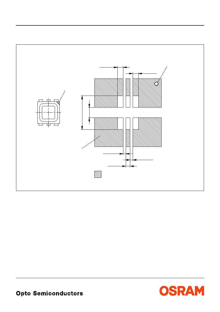
Maþzeichnung
Package Outlines
Maþe werden wie folgt angegeben: mm (inch) / Dimensions are specified as follows: mm (inch).
Gewicht / Approx. weight: 40 mg
GPLY6000
2.8 (0.110)
3.6 (0.142)
3.2 (0.126)
0.6 (0.024)
0.7 (0.028)
0.5 (0.020)
3.5 (0.138)
(2.5 (0.098))
2 (0.079)
0...0.15 (0.006)
A3
A1
C3
C1
A2
C2
2.8 (0.110)
1.6 (0.063)
3.2 (0.126)
0.9 (0.035)
0.4 (0.016)
3.1 (0.122)
2.6 (0.102)
0.4 (0.016)
0.5 (0.020)
0.3 (0.012)
0.7 (0.028)
0.5 (0.020)
Package marking
C1
C2
C3
A2
A3
A1
C1
Cathode
Amber (A)
A1
Anode
Amber (A)
C2
Cathode
True Green (T)
A2
Anode
True Green (T)
C3
Cathode
Blue (B)
A3
Anode
Blue (B)

2003-11-17
16
LATB G66B
Gurtung / Polarit‰t und Lage
Verpackungseinheit 1000/Rolle, ¯180 mm
oder 4000/Rolle, ¯330 mm
Method of Taping / Polarity and Orientation Packing unit 1000/reel, ¯180 mm
or 4000/reel, ¯330 mm
Maþe werden wie folgt angegeben: mm (inch) / Dimensions are specified as follows: mm (inch).
Anm.: Bez¸glich Trockenverpackung finden Sie weitere Hinweise im Internet und in unserem Short
Form Catalog im Kapitel "Gurtung und Verpackung" unter dem Punkt "Trockenverpackung". Hier
sind Normenbez¸ge, unter anderem ein Auszug der JEDEC-Norm, enthalten.
Note: Regarding dry pack you will find further information in the internet and in the Short Form Catalog
in chapter "Tape and Reel" under the topic "Dry Pack". Here you will also find the normative
references like JEDEC. LˆtbedingungenVorbehandlung nach JEDEC Level 2
Soldering ConditionsPreconditioning acc. to JEDEC Level 2
3.5 (0.138)
4 (0.157)
1.5 (0.059)
2 (0.079)
1.5 (0.059)
12 (0.472)
1.75 (0.069)
2
∞
...3
∞
0.3 (0.012) max.
3.7 (0.146)
OHTY0038
2.05 (0.081)
5.5 (0.217)
C3
A3
C2
A2
A1
C1
8 (0.315)
LATB G66B
2003-11-17
17
Empfohlenes Lˆtpaddesign
IR Reflow Lˆten
Recommended Solder Pad
IR Reflow Soldering
Maþe werden wie folgt angegeben: mm (inch) / Dimensions are specified as follows: mm (inch).
Geh‰use h‰lt TTW-Lˆthitze aus / Package able to withstand TTW-soldering heat
0.8 (0.031)
0.8 (0.031)
0.35 (0.014)
Kathoden Markierung
Cathode marking
Solder resist
Lˆtstoplack
improved heat dissipation
16 mm per cath. pad for
2
OHPY0029
C3
A3 A1
A2
C2
C1
Kathoden Markierung
Cathode marking
1.4 (0.055)
4.7 (0.185)
0.35 (0.014)
0.6 (0.024)
2003-11-17
18
LATB G66B
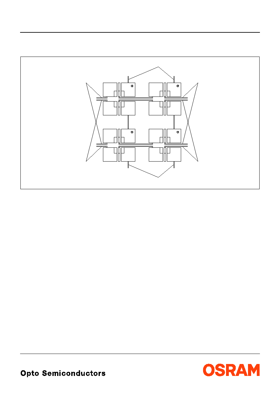
Empfohlenes Platinendesign f¸r cluster mit 6-lead TOPLED
Æ
in Serienschaltung
Recommended PCB-Design for cluster with 6-lead TOPLED
Æ
in Series Connection
OHPY0034
Color 1 cathode
Color 3 cathode
Color 2 cathode
Color 1 anode
Color 2 anode
Color 3 anode
LATB G66B
2003-11-17
19
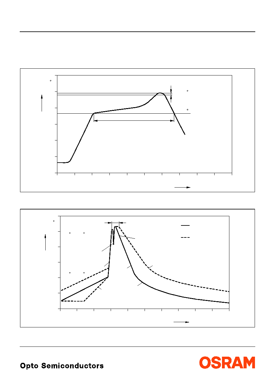
Lˆtbedingungen
Vorbehandlung nach JEDEC Level 2
Soldering Conditions
Preconditioning acc. to JEDEC Level 2
IR-Reflow Lˆtprofil
(nach IPC 9501)
IR Reflow Soldering Profile
(acc. to IPC 9501)
Wellenlˆten (TTW)
(nach CECC 00802)
TTW Soldering
(acc. to CECC 00802)
OHLY0597
0
0
50
100
150
200
250
50
100
150
200
250
300
T
t
C
s
240-245 C
10-40 s
183 C
120 to 180 s
defined for Preconditioning: up to 6 K/s
ramp-down rate up to 6 K/s
ramp-up rate up to 6 K/s
defined for Preconditioning: 2-3 K/s
OHLY0598
0
0
50
100
150
200
250
50
100
150
200
250
300
T
t
C
s
235 C
10 s
C
... 260
1. Welle
1. wave
2. Welle
2. wave
5 K/s
2 K/s
ca 200 K/s
C
C
... 130
100
2 K/s
Zwangsk¸hlung
forced cooling
Normalkurve
standard curve
Grenzkurven
limit curves

2003-11-17
20
LATB G66B
Published by OSRAM Opto Semiconductors GmbH
Wernerwerkstrasse 2, D-93049 Regensburg
© All Rights Reserved.
Attention please!
The information describes the type of component and shall not be considered as assured characteristics.
All typical data and graphs are basing on representative samples, but don't represent the production range. If requested,
e.g. because of technical improvements, these typ. data will be changed without any further notice.
Terms of delivery and rights to change design reserved. Due to technical requirements components may contain
dangerous substances. For information on the types in question please contact our Sales Organization.
If printed or downloaded, please find the latest version in the Internet.
Packing
Please use the recycling operators known to you. We can also help you ≠ get in touch with your nearest sales office.
By agreement we will take packing material back, if it is sorted. You must bear the costs of transport. For packing
material that is returned to us unsorted or which we are not obliged to accept, we shall have to invoice you for any costs
incurred.
Components used in life-support devices or systems must be expressly authorized for such purpose! Critical
components
1
may only be used in life-support devices or systems
2
with the express written approval of OSRAM OS.
1
A critical component is a component used in a life-support device or system whose failure can reasonably be expected
to cause the failure of that life-support device or system, or to affect its safety or the effectiveness of that device or
system.
2
Life support devices or systems are intended (a) to be implanted in the human body, or (b) to support and/or maintain
and sustain human life. If they fail, it is reasonable to assume that the health of the user may be endangered.
Revision History: 2003-11-17
Date of change
Previous Version:
2003-10-29
Page
Subjects (major changes)
9
true green and blue: new dominant wavelength diagrams
2002-12-17
2, 5
new luminous intensity groups
2003-02-11
7
diagram forward current OHL01382 replaced by OHL00590
2003-02-12
14
note: dry pack
2003-08-27
1
ESD norm
2003-08-27
3
ambient temperature
2003-08-27
2, 5
new luminous intensity groups
2003-10-10
2
new ordering codes
2003-10-29