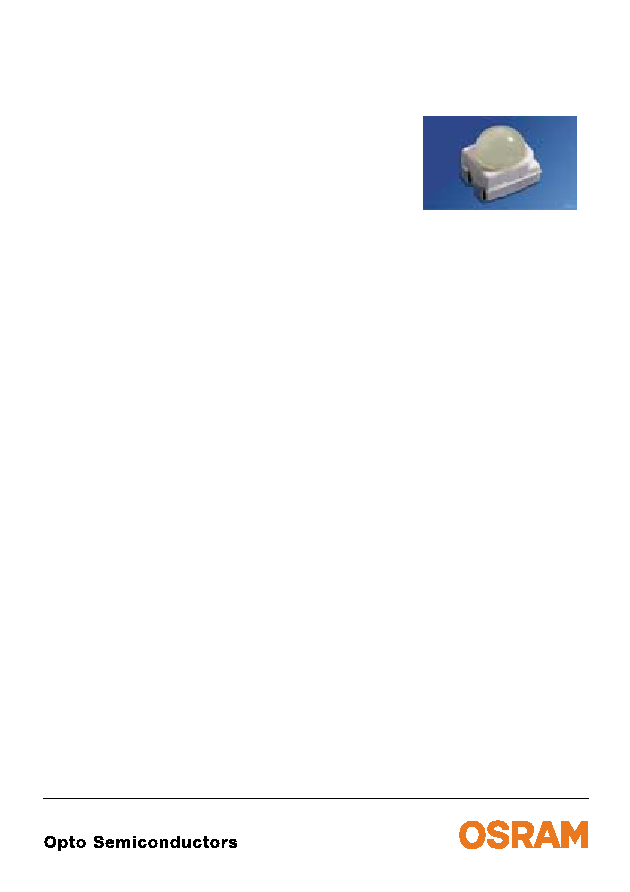
LB E633, LV E633, LT E633
Power TOPLED
Æ
with Lens
Hyper-Bright LED
Abgek¸ndigt nach PD_078_02 - werden durch
LB_LT_LV E63C ersetzt werden
Obsolete acc. to PD_078_02 - will be replaced by
LB_LT_LV E63C
2003-08-26
1
Besondere Merkmale
∑ Geh‰usetyp: weiþes P-LCC-4 Geh‰use mit
Linse
∑ Besonderheit des Bauteils: mehr Licht durch
engen Abstrahlwinkel
∑ Wellenl‰nge: 469 nm (blau), 503 nm (verde),
525 nm (true green)
∑ Abstrahlwinkel: 30∞
∑ Technologie: InGaN
∑ optischer Wirkungsgrad: 2 lm/W (blau),
6 lm/W (verde), 8 lm/W (true green)
∑ Gruppierungsparameter: Lichtst‰rke,
Wellenl‰nge
∑ Verarbeitungsmethode: f¸r alle
SMT-Best¸cktechniken geeignet
∑ Lˆtmethode: IR Reflow Lˆten und
Wellenlˆten (TTW)
∑ Vorbehandlung: nach JEDEC Level 2
∑ Gurtung: 12 mm Gurt mit 2000/Rolle,¯330 mm
∑ ESD-Festigkeit: ESD-sicher bis 2 kV nach
EOS/ESD-5.1-1993
Anwendungen
∑ Ampelanwendung
∑ Hinterleuchtung (LCD, Schalter, Tasten,
Displays, Werbebeleuchtung)
∑ Innenbeleuchtung im Automobilbereich
(z.B. Instrumentenbeleuchtung, u. ‰.)
∑ Ersatz von Kleinst-Gl¸hlampen
∑ Markierungsbeleuchtung (z.B. Stufen,
Fluchtwege, u.‰.)
∑ Signal- und Symbolleuchten
∑ Scanner
Features
∑ package: white P-LCC-4 package with lens
∑ feature of the device: more brightness due to
narrow viewing angle
∑ wavelength: 469 nm (blue), 503 nm (verde),
525 nm (true green)
∑ viewing angle: 30∞
∑ technology: InGaN
∑ optical efficiency: 2 lm/W (blue),
6 lm/W (verde), 8 lm/W (true green)
∑ grouping parameter: luminous intensity,
wavelength
∑ assembly methods: suitable for all
SMT assembly methods
∑ soldering methods:IR reflow soldering and
TTW soldering
∑ preconditioning: acc. to JEDEC Level 2
∑ taping: 12 mm tape with 2000/reel, ¯330 mm
∑ ESD-withstand voltage: up to 2 kV acc. to
EOS/ESD-5.1-1993
Applications
∑ traffic lights
∑ backlighting (LCD, switches, keys, displays,
illuminated advertising)
∑ interior automotive lighting (e.g. dashboard
backlighting, etc.)
∑ substitution of micro incandescent lamps
∑ marker lights (e.g. steps, exit ways, etc.)
∑ signal and symbol luminaire
∑ scanners
2003-08-26
2
LB E633, LV E633, LT E633
Helligkeitswerte werden mit einer Stromeinpr‰gedauer von 25 ms und einer Genauigkeit von ±11 % ermittelt.
Luminous intensity is tested at a current pulse duration of 25 ms and a tolerance of ±11 %.
s
Abgek¸ndigt nach PD_078_02 - werden durch LB_LT_LV E63C ersetzt werden
Obsolete acc. to PD_078_02 - will be replaced by LB_LT_LV E63C
Letzte Bestellung / Last Order: 30.09.2003
Letzte Lieferung / Last Delivery: 31.03.2004
Anm.: -1 gesamter Farbbereich, Lieferung in Einzelgruppen (siehe Seite 5)
Die Standardlieferform von Serientypen beinhaltet eine untere bzw. eine obere Familiengruppe,
die aus nur 3 bzw. 4 Halbgruppen besteht. Einzelne Halbgruppen sind nicht erh‰ltlich.
In einer Verpackungseinheit / Gurt ist immer nur eine Halbgruppe enthalten.
Note: -1 Total color tolerance range, delivery in single groups (please see page 5)
The standard shipping format for serial types includes a lower or upper family group of 3 or 4
individual groups. Individual half groups are not available.
No packing unit / tape ever contains more than one luminous intensity half group.
Typ
Type
Emissions-
farbe
Color of
Emission
Farbe der
Lichtaustritts-
fl‰che
Color of the
Light Emitting
Area
Lichtst‰rke
Luminous
Intensity
I
F
= 30 mA
I
V
(mcd)
Lichtstrom
Luminous
Flux
I
F
= 30 mA
V
(mlm)
Bestellnummer
Ordering Code
s
LB E633-Q1R1-1
s
LB E633-R1S2-1
blue
colorless clear
71 ... 140
112 ... 280
120 (typ.)
220 (typ.)
on request
s
LV E633-U1V1-1
s
LV E633-V1AB-1
verde
colorless clear
450 ... 900
710 ...1800
390 (typ.)
700 (typ.)
on request
s
LT E633-U1V1-1
s
LT E633-V1AB-1
true green
colorless clear
450 ... 900
710 ...1800
390 (typ.)
700 (typ.)
on request
LB E633, LV E633, LT E633
2003-08-26
3
Grenzwerte
Maximum Ratings
Bezeichnung
Parameter
Symbol
Symbol
Werte
Values
Einheit
Unit
LB
LV, LT
Betriebstemperatur
Operating temperature range
T
op
≠ 40 ... + 100
∞C
Lagertemperatur
Storage temperature range
T
stg
≠ 40 ... + 100
∞C
Sperrschichttemperatur
Junction temperature
T
j
+110
+125
∞C
Durchlassstrom
Forward current
I
F
30
mA
Stoþstrom
Surge current
t
10
µ
s,
D
= 0.005
I
FM
200
250
mA
Sperrspannung
Reverse voltage
V
R
5
V
Leistungsaufnahme
Power consumption
P
tot
120
mW
W‰rmewiderstand
Thermal resistance
Sperrschicht/Umgebung
Junction/ambient
Sperrschicht/Lˆtpad
Junction/solder point
Montage auf PC-Board FR 4 (Padgrˆþe
16 mm
2
)
mounted on PC board FR 4 (pad size
16 mm
2
)
R
th JA
R
th JS
300
130
K/W
K/W
2003-08-26
4
LB E633, LV E633, LT E633
Kennwerte (
T
A
= 25 ∞C)
Characteristics
Bezeichnung
Parameter
Symbol
Symbol
Werte
Values
Einheit
Unit
LB
LV
LT
Wellenl‰nge des emittierten Lichtes
(typ.)
Wavelength at peak emission
I
F
= 30 mA
peak
464
501
520
nm
Dominantwellenl‰nge
1)
(typ.)
Dominant wavelength
I
F
= 30 mA
dom
469
± 6
503
± 6
525
± 9
nm
Spektrale Bandbreite bei 50 %
I
rel max
(typ.)
Spectral bandwidth at 50 %
I
rel max
I
F
= 30 mA
25
30
33
nm
Abstrahlwinkel bei 50 %
I
V
(Vollwinkel)
(typ.)
Viewing angle at 50 %
I
V
2
30
30
30
Grad
deg.
Durchlassspannung
2)
(min.)
Forward voltage
(typ.)
I
F
= 30 mA
(max.)
V
F
V
F
V
F
3.1
3.7
4.0
3.1
3.5
4.0
3.1
3.5
4.0
V
V
V
Sperrstrom
(typ.)
Reverse current
(max.)
V
R
= 5 V
I
R
I
R
0.01
10
0.01
10
0.01
10
µ
A
µ
A
Temperaturkoeffizient von
peak
(typ.)
Temperature coefficient of
peak
I
F
= 30 mA; ≠10∞C
T
100∞C
TC
peak
0.04
0.03
0.04
nm/K
Temperaturkoeffizient von
dom
(typ.)
Temperature coefficient of
dom
I
F
= 30 mA; ≠10∞C
T
100∞C
TC
dom
0.03
0.04
0.03
nm/K
Temperaturkoeffizient von
V
F
(typ.)
Temperature coefficient of
V
F
I
F
= 30 mA; ≠10∞C
T
100∞C
TC
V
≠ 4.5
≠ 3.6
≠ 3.6
mV/K
Optischer Wirkungsgrad
(typ.)
Optical efficiency
I
F
= 30 mA
opt
2
6
8
lm/W
1)
Wellenl‰ngengruppen werden mit einer Stromeinpr‰gedauer von 25 ms und einer Genauigkeit von ±1 nm ermittelt.
Wavelength groups are tested at a current pulse duration of 25 ms and a tolerance of ±1 nm.
2)
Durchlassspannungsgruppen werden mit einer Stromeinpr‰gedauer von 1 ms und einer Genauigkeit von ±0,05 V
ermittelt.
Forward voltage groups are tested at a current pulse duration of 1 ms and a tolerance of ±0.05 V.
LB E633, LV E633, LT E633
2003-08-26
5
Helligkeitswerte werden mit einer Stromeinpr‰gedauer von 25 ms und einer Genauigkeit von
±
11% ermittelt.
Luminous intensity is tested at a current pulse duration of 25 ms and a tolerance of
±
11%.
1)
Wellenl‰ngengruppen / Wavelength groups
Gruppe
Group
blue
verde
true green
Einheit
Unit
min.
max. min.
max. min.
max.
3
463
467
497
501
516
522
nm
4
467
471
501
505
522
528
nm
5
471
475
505
509
528
534
nm
Helligkeits-Gruppierungsschema
Luminous Intensity Groups
Lichtgruppe
Luminous Intensity Group
Lichtst‰rke
Luminous Intensity
I
V
(mcd)
Lichtstrom
Luminous Flux
V
(mlm)
Q1
Q2
R1
R2
S1
S2
T1
T2
U1
U2
V1
V2
AA
AB
71.0 ...
90.0
90.0 ...
112.0
112.0 ...
140.0
140.0 ...
180.0
180.0 ...
224.0
224.0 ...
280.0
280.0 ...
355.0
355.0 ...
450.0
450.0 ...
560.0
560.0 ...
710.0
710.0 ...
900.0
900.0 ... 1120.0
1120.0 ... 1400.0
1400.0 ... 1800.0
240 (typ.)
300 (typ.)
380 (typ.)
480 (typ.)
600 (typ.)
760 (typ.)
950 (typ.)
1200 (typ.)
1500 (typ.)
1900 (typ.)
2400 (typ.)
3000 (typ.)
3700 (typ.)
4800 (typ.)
Gruppenbezeichnung auf Etikett
Group Name on Label
Beispiel: S2-3
Example: S2-3
Lichtgruppe
Luminous Intensity Group
Halbgruppe
Half Group
Wellenl‰nge
Wavelength
S
2
3
2003-08-26
6
LB E633, LV E633, LT E633
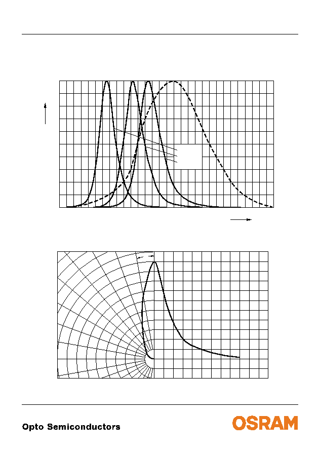
Relative spektrale Emission
I
rel
=
f
(
),
T
A
= 25 ∞C,
I
F
= 30 mA
Relative Spectral Emission
V(
) = spektrale Augenempfindlichkeit
Standard eye response curve
Abstrahlcharakteristik
I
rel
=
f
(
)
Radiation Characteristic
0
400
true green
550
450
500
600
650
nm
700
OHL00492
I
20
40
60
80
%
100
rel
verde
blue
V
0
0.2
0.4
1.0
0.6
1.0
0.8
0.6
0.4
0∞
10∞
20∞
40∞
30∞
OHL00744
50∞
60∞
70∞
80∞
90∞
100∞
0∞
20∞
40∞
60∞
80∞
100∞
120∞
LB E633, LV E633, LT E633
2003-08-26
7
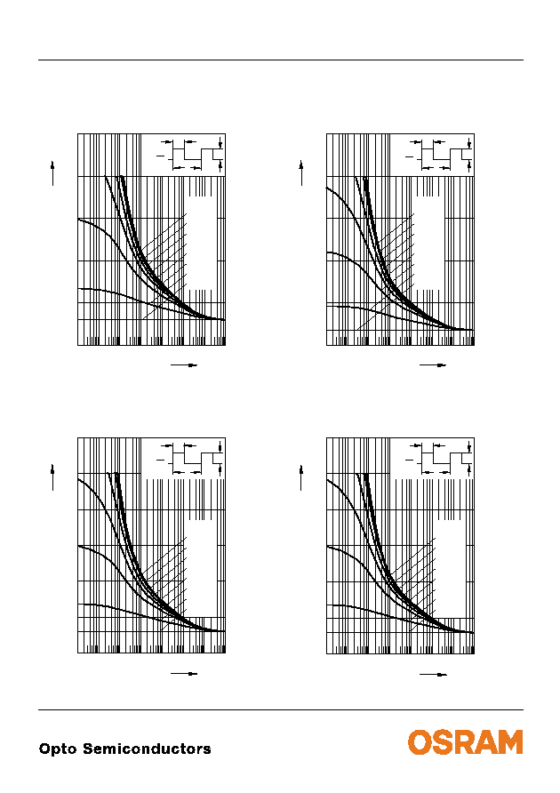
Durchlassstrom
I
F
=
f
(
V
F
)
Forward Current
T
A
= 25 ∞C
Maximal zul‰ssiger Durchlassstrom
I
F
=
f
(
T
)
Max. Permissible Forward Current
Relative Lichtst‰rke
I
V
/
I
V(30 mA)
=
f
(
I
F
)
Relative Luminous Intensity
T
A
= 25 ∞C
Maximal zul‰ssiger Durchlassstrom
I
F
=
f
(
T
)
Max. Permissible Forward Current
OHL00495
10
-1
2.5
3
3.5
4
4.5 V 5
0
10
1
10
10
2
5
5
mA
5
2
true green
verde,
blue
I
F
V
F
true green
60
0
0
40
20
temp. ambient
T
A
verde,
F
I
mA
blue
100
80 ∞C
T
OHL01311
5
10
15
20
25
30
35
OHL00686
10
-2
-1
10
0
10
10
1
5
5
-1
10
10
0
10
1
10
mA
2
I
F
V
V (30 mA)
I
I
true green
verde
blue
true green
60
0
0
40
20
temp. solder point
T
S
verde,
F
I
mA
blue
100
80 ∞C
T
OHL01310
5
10
15
20
25
30
35
LB E633, LV E633, LT E633
2003-08-26
8
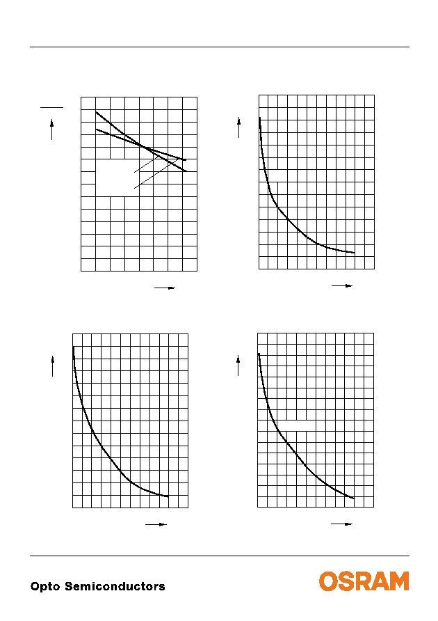
Relative Lichtst‰rke
I
V
/
I
V(25 ∞C)
=
f
(
T
A
)
Relative Luminous Intensity
I
F
= 30 mA
Dominante Wellenl‰nge
dom
=
f
(
I
F
)
Dominant Wavelength
LV
, T
A
= 25 ∞C
Dominante Wellenl‰nge
dom
=
f
(
I
F
)
Dominant Wavelength
LB
, T
A
= 25 ∞C
Dominante Wellenl‰nge
dom
=
f
(
I
F
)
Dominant Wavelength
LT
, T
A
= 25 ∞C
OHL03637
-60
0
T
∞C
V (25 ∞C)
I
I
V
-40 -20
0
20 40 60
100
0.2
0.4
0.6
0.8
1.0
1.2
1.4
true green
blue
verde
I
OHL10198
498
dom
0
mA
nm
20
40
60
80
120
500
502
504
506
508
510
512
I
OHL10196
467
dom
0
mA
nm
20
40
60
80
120
468
469
470
471
472
473
474
blue
f
I
OHL00882
510
dom
0
mA
nm
20
40
60
80
120
515
520
525
530
535
540
550
f
true green
LB E633, LV E633, LT E633
2003-08-26
9
Zul‰ssige Impulsbelastbarkeit
I
F
=
f
(
t
p
)
Permissible Pulse Handling Capability
Duty cycle
D
= parameter,
T
A
= 25 ∞C
LB
Zul‰ssige Impulsbelastbarkeit
I
F
=
f
(
t
p
)
Permissible Pulse Handling Capability
Duty cycle
D
= parameter,
T
A
= 25 ∞C
LV, LT
Zul‰ssige Impulsbelastbarkeit
I
F
=
f
(
t
p
)
Permissible Pulse Handling Capability
Duty cycle
D
= parameter,
T
A
= 85 ∞C
LB
Zul‰ssige Impulsbelastbarkeit
I
F
=
f
(
t
p
)
Permissible Pulse Handling Capability
Duty cycle
D
= parameter,
T
A
= 85 ∞C
LV, LT
OHL01957
10
-5
p
t
F
I
10
-4
10
-3
10
-2
10
-1
10
0
10
1
0
A
2
10
s
D
t
P
T
=
T
P
t
I
F
0.01
0.05
0.2
0.1
0.005
0.02
0.5
D
=
1
0.05
0.10
0.15
0.25
OHL01959
10
-5
p
t
F
I
10
-4
10
-3
10
-2
10
-1
10
0
10
1
0
A
2
10
s
D
t
P
T
=
T
P
t
I
F
0.01
0.05
0.2
0.1
0.005
0.02
0.5
D
=
1
0.05
0.10
0.15
0.20
0.30
OHL01958
10
-5
p
t
F
I
10
-4
10
-3
10
-2
10
-1
10
0
10
1
0
A
2
10
s
D
t
P
T
=
T
P
t
I
F
0.01
0.05
0.2
0.1
0.005
0.02
0.5
D
=
1
0.05
0.10
0.15
0.25
OHL01960
10
-5
p
t
F
I
10
-4
10
-3
10
-2
10
-1
10
0
10
1
0
A
2
10
s
D
t
P
T
=
T
P
t
I
F
0.01
0.05
0.2
0.1
0.005
0.02
0.5
D
=
1
0.05
0.10
0.15
0.20
0.30
2003-08-26
10
LB E633, LV E633, LT E633
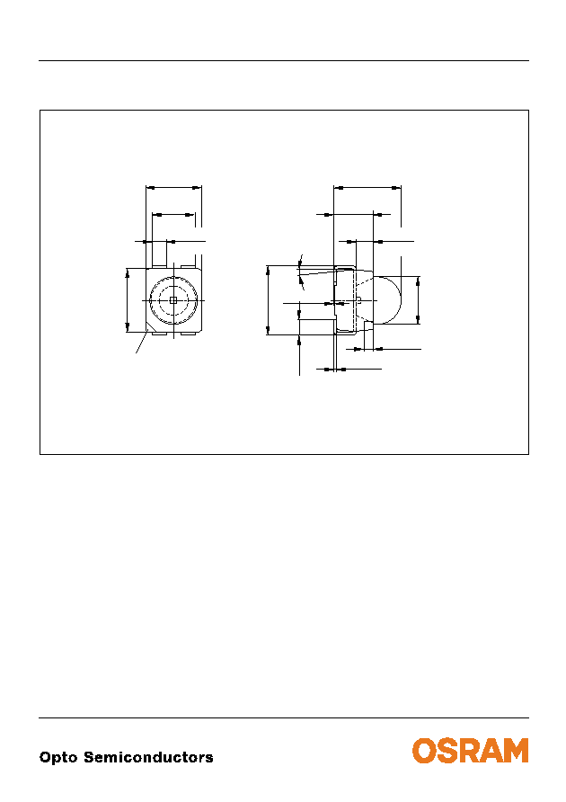
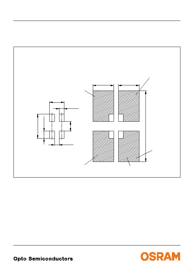
Maþzeichnung
Package Outlines
Maþe werden wie folgt angegeben: mm (inch) / Dimensions are specified as follows: mm (inch).
Gewicht / Approx. weight: 38 mg
3.5 (0.138) max.
¯
2.55 (0.100)
0.13 (0.005)
0.18 (0.007)
0.1 (0.004) typ
marking
Package
1.1 (0.043)
0.5 (0.020)
2.6 (0.102)
3.4 (0.134)
3.0 (0.118)
2.1 (0.083)
2.3 (0.091)
3.0 (0.118)
3.7 (0.146)
3.3 (0.130)
4
∞
±1
GPLY7000
0.4 (0.016)
0.6 (0.024)
0.9 (0.035)
0.7 (0.028)
1.7 (0.067)
2.1 (0.083)
0.6 (0.024)
0.8 (0.031)
A
C
C
C
¯
2.60 (0.102)
LB E633, LV E633, LT E633
2003-08-26
11
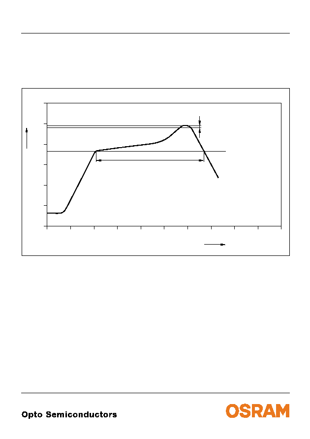
Lˆtbedingungen
Vorbehandlung nach JEDEC Level 2
Soldering Conditions Preconditioning acc. to JEDEC Level 2
IR-Reflow Lˆtprofil
(nach IPC 9501)
IR Reflow Soldering Profile
(acc. to IPC 9501)
OHLY0597
0
0
50
100
150
200
250
50
100
150
200
250
300
T
t
∞C
s
240-245 ∞C
10-40 s
183 ∞C
120 to 180 s
Defined for Preconditioning: up to 6 K/s
Ramp-down rate up to 6 K/s
Ramp-up rate up to 6 K/s
Defined for Preconditioning: 2-3 K/s
2003-08-26
12
LB E633, LV E633, LT E633
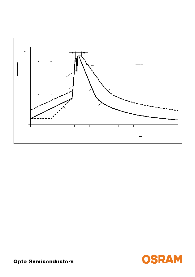
Wellenlˆten (TTW)
(nach CECC 00802)
TTW Soldering
(acc. to CECC 00802)
OHLY0598
0
0
50
100
150
200
250
50
100
150
200
250
300
T
t
C
s
235 C
10 s
C
... 260
1. Welle
1. wave
2. Welle
2. wave
5 K/s
2 K/s
ca 200 K/s
C
C
... 130
100
2 K/s
Zwangsk¸hlung
forced cooling
Normalkurve
standard curve
Grenzkurven
limit curves
LB E633, LV E633, LT E633
2003-08-26
13
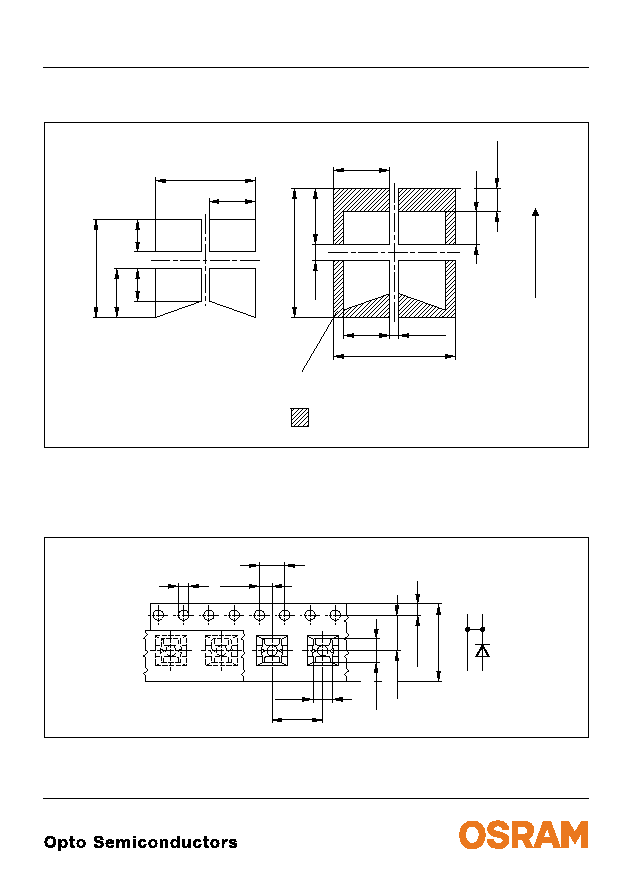
Empfohlenes Lˆtpaddesign verwendbar f¸r TOPLED
Æ
und Power TOPLED
Æ
IR Reflow Lˆten
Recommended Solder Pad useable for TOPLED
Æ
and Power TOPLED
Æ
IR Reflow Soldering
Maþe werden wie folgt angegeben: mm (inch) / Dimensions are specified as follows: mm (inch).
Padgeometrie f¸r
verbesserte W‰rmeableitung
improved heat dissipation
Paddesign for
Lˆt t l k
0.8 (0.031)
3.7 (0.146)
1.1 (0.043)
2.3 (0.091)
3.3 (0.130)
1.5 (0.059)
11.1 (0.437)
Cu Fl‰che / 16 mm per pad
2
Cu-area
_
<
3.3 (0.130)
Kathode/
Cathode
Anode
Fl‰che darf elektrisch nicht beschaltet werden.
Do not use this area for electrical contact.
0.7 (0.028)
Fl‰che darf elektrisch nicht beschaltet werden.
Do not use this area for electrical contact.
2003-08-26
14
LB E633, LV E633, LT E633
Empfohlenes Lˆtpaddesign
Wellenlˆten (TTW)
Recommended Solder Pad
TTW Soldering
Maþe werden wie folgt angegeben: mm (inch) / Dimensions are specified as follows: mm (inch).
Gurtung / Polarit‰t und Lage
Verpackungseinheit 2000/Rolle, ¯330 mm
Method of Taping / Polarity and Orientation Packing unit 2000/reel, ¯330 mm
Maþe werden wie folgt angegeben: mm (inch) / Dimensions are specified as follows: mm (inch).
OHAY0583
6.1 (0.240)
2.8 (0.110)
2 (0.079)
3 (0.118)
6 (0.236)
3.5 (0.138)
1.5 (0.059)
2 (0.079)
3.5 (0.138)
1 (0.039)
8 (0.315)
2.8 (0.110)
0.5 (0.020)
7.5 (0.295)
Solder resist
Lˆtstoplack
PCB-direction
Bewegungsrichtung
der Platine
2 (0.079)
Padgeometrie f¸r
improved heat dissipation
verbesserte W‰rmeableitung
Paddesign for
2
Cu Fl‰che / > 12 mm per pad
Cu-area
OHAY0734
C
A
C
C
1.5 (0.059)
2 (0.079)
4 (0.157)
3 (0.118)
3.8 (0.150)
5.5 (0.217)
1.75 (0.069)
12 (0.472)
8 (0.315)
LB E633, LV E633, LT E633
2003-08-26
15
Published by OSRAM Opto Semiconductors GmbH & Co. OHG
Wernerwerkstrasse 2, D-93049 Regensburg
© All Rights Reserved.
Attention please!
The information describes the type of component and shall not be considered as assured characteristics.
Terms of delivery and rights to change design reserved. Due to technical requirements components may contain
dangerous substances. For information on the types in question please contact our Sales Organization.
If printed or downloaded, please find the latest version in the Internet.
Packing
Please use the recycling operators known to you. We can also help you ≠ get in touch with your nearest sales office.
By agreement we will take packing material back, if it is sorted. You must bear the costs of transport. For packing
material that is returned to us unsorted or which we are not obliged to accept, we shall have to invoice you for any costs
incurred.
Components used in life-support devices or systems must be expressly authorized for such purpose! Critical
components
1
may only be used in life-support devices or systems
2
with the express written approval of OSRAM OS.
1
A critical component is a component used in a life-support device or system whose failure can reasonably be expected
to cause the failure of that life-support device or system, or to affect its safety or the effectiveness of that device or
system.
2
Life support devices or systems are intended (a) to be implanted in the human body, or (b) to support and/or maintain
and sustain human life. If they fail, it is reasonable to assume that the health of the user may be endangered.
Revision History: 2003-08-26
Date of change
Previous Version:
2003-08-07
Page
Subjects (major changes since last revision)
4
value (forward voltage)
1, 2
Obsolete
2003-08-07