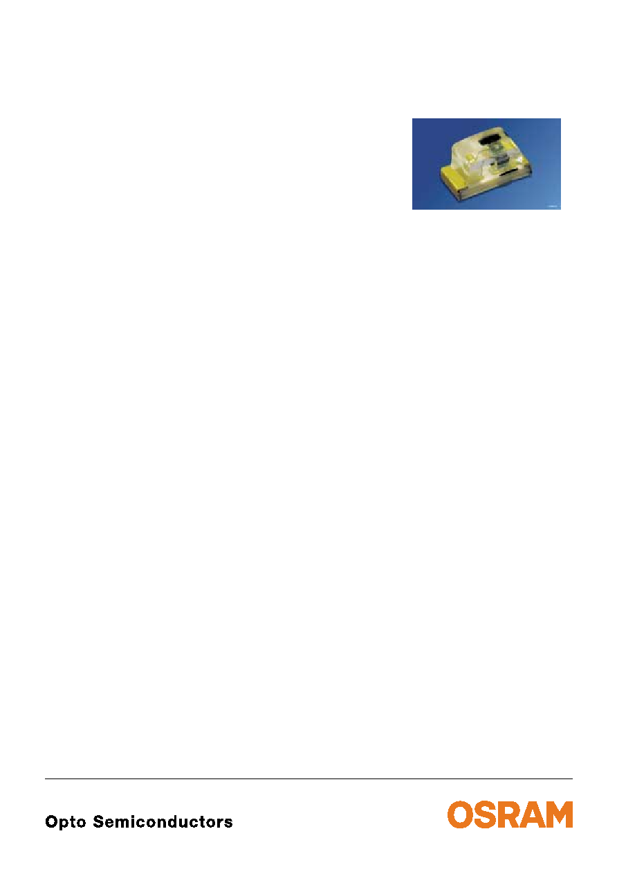
LB Q993
Hyper CHIPLED
Hyper-Bright LED
Abgek¸ndigt nach OS-PD-2003-007 - wird durch
LB L293 ersetzt werden
Obsolete acc. to OS-PD-2003-007 - will be replaced by
LB L293
2003-08-27
1
Besondere Merkmale
∑ Geh‰usetyp: SMT Geh‰use 0603
∑ Besonderheit des Bauteils: kleinste Bauform
1,6 x 0,8 x 0,8 mm (LxBxH)
∑ Wellenl‰nge: 470 nm (blau)
∑ Abstrahlwinkel: extrem breite
Abstrahlcharakteristik (160∞)
∑ Technologie: InGaN
∑ optischer Wirkungsgrad: 2 lm/W
∑ Gruppierungsparameter: Lichtst‰rke;
Wellenl‰nge
∑ Verarbeitungsmethode: f¸r alle
SMT-Best¸cktechniken geeignet
∑ Lˆtmethode: IR Reflow Lˆten
∑ Vorbehandlung: nach JEDEC Level 2
∑ Gurtung: 8 mm Gurt mit 4000/Rolle, ¯180 mm
∑ ESD-Festigkeit: ESD-sicher bis 2 kV nach
EOS/ESD-5.1-1993
Anwendungen
∑ flache Hinterleuchtung (LCD, Handy, Schalter,
Display)
∑ Spielsachen
∑ Informationsanzeigen im Aussenbereich
∑ Signal- und Symbolleuchten
∑ Markierungsbeleuchtung (Stufen, Fluchtwege
u. ‰.)
Features
∑ package: SMT package 0603
∑ feature of the device: smallest
package 1.6 x 0.8 x 0.8 mm (LxWxH)
∑ wavelength: 470 nm (blue)
∑ viewing angle: extremely wide (160∞)
∑ technology: InGaN
∑ optical efficiency: 2 lm/W
∑ grouping parameter: luminous intensity;
Wavelength
∑ assembly methods: suitable for all
SMT assembly methods
∑ soldering methods: IR reflow soldering
∑ preconditioning: acc. to JEDEC Level 2
∑ taping: 8 mm tape with 4000/reel, ¯180 mm
∑ ESD-withstand voltage: up to 2 kV acc. to
EOS/ESD-5.1-1993
Applications
∑ flat backlighting (LCD, cellular phones,
switches, displays)
∑ toys
∑ outdoor displays
∑ signal and symbol luminary
∑ marker lights (e.g. steps, exit ways, etc.)

2003-08-27
2
LB Q993
s
Abgek¸ndigt nach OS-PD-2003-007 - wird durch LB L293 ersetzt werden
Obsolete acc. to OS-PD-2003-007 - will be replaced by LB L293
Letzte Bestellung / Last Order: 2003-10-31
Letzte Lieferung / Last Delivery: 2004-03-31
Anm.: -35 gesamter Farbbereich, Lieferung in Einzelgruppen (siehe Seite 5)
Die Standardlieferform von Serientypen beinhaltet eine untere bzw. eine obere Familiengruppe,
die aus nur zwei bzw. drei Gruppen besteht. Einzelne Gruppen sind nicht erh‰ltlich.
In einer Verpackungseinheit / Gurt ist immer nur eine Gruppe enthalten.
Note: -35 Total color tolerance range, delivery in single groups (please see page 5)
The standard shipping format for serial types includes a lower or upper family group of two or
three groups. Individual groups are not available.
No packing unit / tape ever contains more than one luminous intensity group.
Typ
Type
Emissions-
farbe
Color of
Emission
Farbe der
Lichtaustritts-
fl‰che
Color of the
Light Emitting
Area
Lichtst‰rke
Luminous
Intensity
I
F
= 10 mA
I
V
(mcd)
Lichtstrom
Luminous
Flux
I
F
= 10 mA
V
(mlm)
Bestellnummer
Ordering Code
s
LB Q993-JK-35
s
LB Q993-KM-35
blue
colorless clear
4.5 ... 11.2
7.1 ... 28.0
40 (typ.)
85 (typ.)
Q62702P5438
Q62702P5439
LB Q993
2003-08-27
3
Grenzwerte
Maximum Ratings
Bezeichnung
Parameter
Symbol
Symbol
Wert
Value
Einheit
Unit
Betriebstemperatur
Operating temperature range
T
op
≠ 30 ... + 85
∞C
Lagertemperatur
Storage temperature range
T
stg
≠ 40 ... + 85
∞C
Sperrschichttemperatur
Junction temperature
T
j
+ 95
∞C
Durchlassstrom
Forward current
I
F
15
mA
Stoþstrom
Surge current
t
=
10
µ
s,
D
= 0.1
I
FM
0.1
A
Sperrspannung
Reverse voltage
1)
V
R
5
V
Leistungsaufnahme
Power consumption
P
tot
60
mW
W‰rmewiderstand
Thermal resistance
Sperrschicht/Umgebung
Junction/ambient
Sperrschicht/Lˆtpad
Junction/solder point
Montage auf PC-Board FR 4 (Padgrˆþe
5 mm
2
)
mounted on PC board FR 4 (pad size
5 mm
2
)
R
th JA
R
th JS
650
370
K/W
K/W
1)
f¸r kurzzeitigen Betrieb geeignet / suitable for short term application
2003-08-27
4
LB Q993
Kennwerte (
T
A
= 25 ∞C)
Characteristics
Bezeichnung
Parameter
Symbol
Symbol
Wert
Value
Einheit
Unit
Wellenl‰nge des emittierten Lichtes
(typ.)
Wavelength at peak emission
I
F
= 10 mA
peak
465
nm
Dominantwellenl‰nge
1)
(typ.)
Dominant wavelength
I
F
= 10 mA
dom
470 ± 6
nm
Spektrale Bandbreite bei 50 %
I
rel max
(typ.)
Spectral bandwidth at 50 %
I
rel max
I
F
= 10 mA
25
nm
Abstrahlwinkel bei 50 %
I
V
(Vollwinkel)
(typ.)
Viewing angle at 50 %
I
V
2
160
Grad
deg.
Durchlassspannung
2)
(typ.)
Forward voltage
(max.)
I
F
= 10 mA
V
F
V
F
3.4
3.9
V
V
Sperrstrom
(typ.)
Reverse current
(max.)
V
R
= 5 V
I
R
I
R
0.01
10
µ
A
µ
A
Temperaturkoeffizient von
peak
(typ.)
Temperature coefficient of
peak
I
F
= 10 mA; ≠10∞C
T
100∞C
TC
peak
0.04
nm/K
Temperaturkoeffizient von
dom
(typ.)
Temperature coefficient of
dom
I
F
= 10 mA; ≠10∞C
T
100∞C
TC
dom
0.02
nm/K
Temperaturkoeffizient von
V
F
(typ.)
Temperature coefficient of
V
F
I
F
= 10 mA; ≠10∞C
T
100∞C
TC
VF
≠ 2.9
mV/K
Optischer Wirkungsgrad
(typ.)
Optical efficiency
I
F
= 10 mA
opt
2
lm/W
1)
Wellenl‰ngengruppen werden mit einer Stromeinpr‰gedauer von 25 ms und einer Genauigkeit von ±1 nm ermittelt.
Wavelength groups are tested at a current pulse duration of 25 ms and a tolerance of ±1 nm.
2)
Spannungswerte werden mit einer Stromeinpr‰gedauer von 1 ms und einer Genauigkeit von ±0,1 V ermittelt.
Voltages are tested at a current pulse duration of 1 ms and a tolerance of ±0.1 V.

LB Q993
2003-08-27
5
Helligkeitswerte werden mit einer Stromeinpr‰gedauer von 25 ms und einer Genauigkeit von
±
11% ermittelt.
Luminous intensity is tested at a current pulse duration of 25 ms and a tolerance of
±
11%.
1)
Wellenl‰ngengruppen / Wavelength groups
Gruppe
Group
blue
Einheit
Unit
min.
max.
3
464
468
nm
4
468
472
nm
5
472
476
nm
Helligkeits-Gruppierungsschema
Luminous Intensity Groups
Lichtgruppe
Luminous Intensity Group
Lichtst‰rke
Luminous Intensity
I
V
(mcd)
Lichtstrom
Luminous Flux
V
(mlm)
J
K
L
M
4.5 ... 7.1
7.1 ... 11.2
11.2 ... 18.0
18.0 ... 28.0
16 (typ.)
26 (typ.)
43 (typ.)
65 (typ.)
Gruppenbezeichnung auf Etikett
Group Name on Label
Beispiel: L-3
Example: L-3
Lichtgruppe
Luminous Intensity Group
Wellenl‰nge
Wavelength
L
3
2003-08-27
6
LB Q993
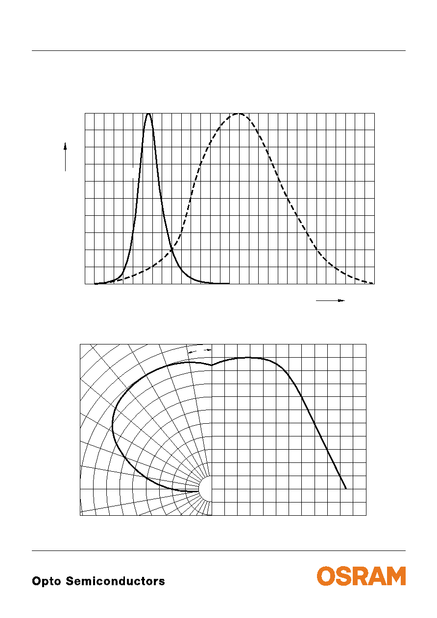
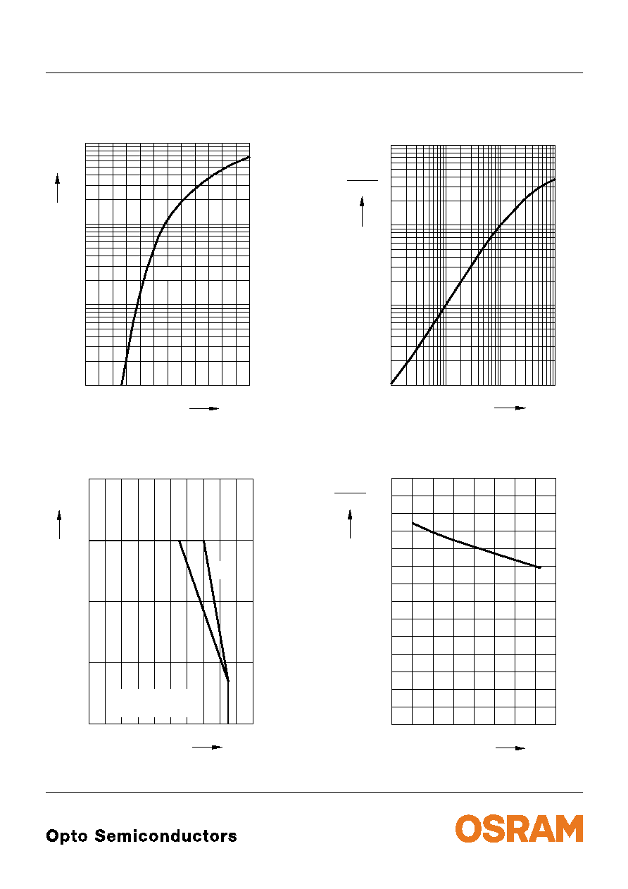
Relative spektrale Emission
I
rel
=
f
(
),
T
A
= 25 ∞C,
I
F
= 10 mA
Relative Spectral Emission
V(
) = spektrale Augenempfindlichkeit
Standard eye response curve
Abstrahlcharakteristik
I
rel
=
f
(
)
Radiation Characteristic
0
400
550
450
500
600
650
nm
700
OHL01492
I
20
40
60
80
%
100
rel
blue
V
0
0.2
0.4
1.0
0.8
0.6
1.0
0.8
0.6
0.4
0∞
10∞
20∞
40∞
30∞
OHL00408
50∞
60∞
70∞
80∞
90∞
100∞
0∞
20∞
40∞
60∞
80∞
100∞
120∞
LB Q993
2003-08-27
7
Durchlassstrom
I
F
=
f
(
V
F
)
Forward Current
T
A
= 25 ∞C
Maximal zul‰ssiger Durchlassstrom
I
F
=
f
(
T
)
Max. Permissible Forward Current
Relative Lichtst‰rke
I
V
/
I
V(10 mA)
=
f
(
I
F
)
Relative Luminous Intensity
T
A
= 25 ∞C
Relative Lichtst‰rke
I
V
/
I
V(25 ∞C)
=
f
(
T
A
)
Relative Luminous Intensity
I
F
= 10 mA
OHL01494
10
-1
2.5
3.0
3.5
4.0
4.5 V 5.0
0
10
1
10
10
2
5
5
mA
5
2.0
blue
I
F
V
F
T
OHL01230
0
F
I
0
20
40
60
80 ∞C 100
mA
temp. solder point
temp. ambient
T
T
S
A
T
A
T
S
5
10
15
20
V
V (10 mA)
10
-1
0
10
10
1
2
10
mA
10
-2
5
OHL01228
1
10
I
I
5
5
10
-1
10
0
5
F
I
OHL01870
-60
0
T
∞C
V (25 ∞C)
I
I
V
-40 -20
0
20 40 60
100
0.2
0.4
0.6
0.8
1.0
1.2
1.4

LB Q993
2003-08-27
8
Dominante W‰llenl‰nge
dom
=
f
(
I
F
)
Dominant wavelength
T
A
= 25 ∞C
Zul‰ssige Impulsbelastbarkeit
I
F
=
f
(
t
p
)
Permissible Pulse Handling Capability
Duty cycle
D
= parameter,
T
A
= 25 ∞C
I
OHL01535
469.0
dom
0
F
10
20
30
40 mA 50
469.5
470.0
470.5
471.0
472.0
nm
blue
468.5
OHL00799
10
-5
p
t
F
I
10
-4
10
-3
10
-2
10
-1
10
0
10
1
0
A
2
10
s
D
t
P
T
=
T
P
t
I
F
0.01
0.05
0.2
0.1
0.005
0.02
0.5
D
=
0.02
0.04
0.06
0.08
0.10
0.12
1

LB Q993
2003-08-27
9
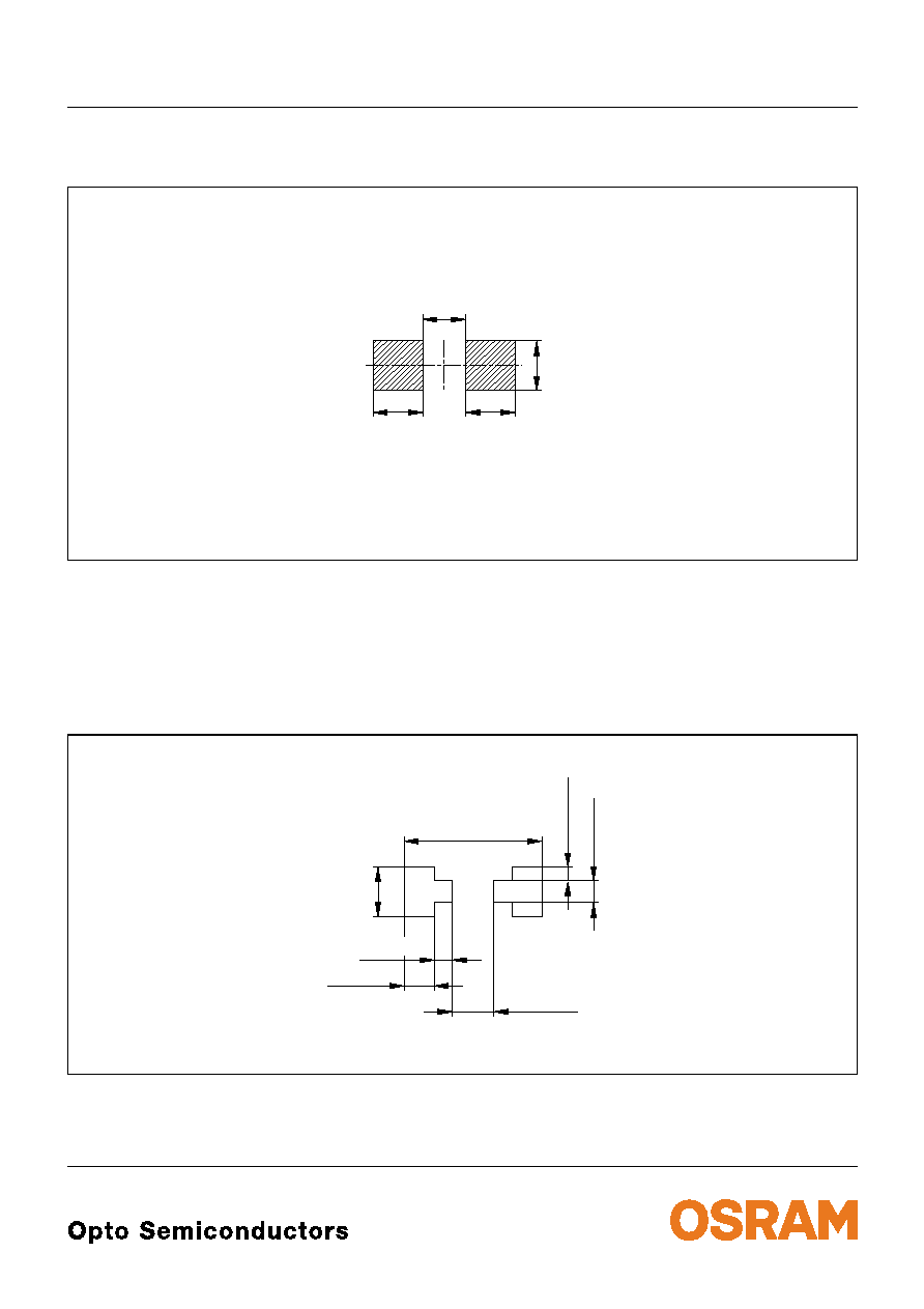
Maþzeichnung
Package Outlines
Maþe werden wie folgt angegeben: mm (inch) / Dimensions are specified as follows: mm (inch).
Gewicht / Approx. weight: 1.4 mg
GEOY6023
Cathode mark
1.7 (0.067)
Cathode mark
0.9 (0.035)
0.9 (0.035)
0.7 (0.028)
1.5 (0.059)
0.7 (0.028)
0.4 (0.016)
0.2 (0.008)
0.2 (0.008)
0.4 (0.016)
1.3 (0.051)
1.1 (0.043)
1.0 (0.039)
1.2 (0.047)

2003-08-27
10
LB Q993
Lˆtbedingungen
Vorbehandlung nach JEDEC Level 2
Soldering Conditions Preconditioning acc. to JEDEC Level 2
IR-Reflow Lˆtprofil
(nach CECC 00802)
IR Reflow Soldering Profile
(acc. to CECC 00802)
OHLA0685
0:00
0
T
t
∞C
min
50
100
150
200
250
0:30
1:00
1:30
2:00
2:30
3:00
3:30
4:00
4:30
5:00
5:30
2-3 K/s
2-3 K/s
T
= 183 ∞C
= 70 s
t
max
T
= 245 ∞C
LB Q993
2003-08-27
11
Empfohlenes Lˆtpaddesign
IR Reflow Lˆten
Recommended Solder Pad
IR Reflow Soldering
Maþe werden wie folgt angegeben: mm (inch) / Dimensions are specified as follows: mm (inch).
Empfohlenes Lˆtpaddesign verwendbar f¸r Hyper CHIPLED und Chipled - Bauform 0603
IR Reflow Lˆten
Recommended Solder Pad useable for Hyper CHIPLED and Chipled - Package 0603
IR Reflow Soldering
Maþe werden wie folgt angegeben: mm (inch) / Dimensions are specified as follows: mm (inch).
Empfohlene Lˆtpastendicke: 120 µm/ recommended thickness of solder paste: 120 µm
0.8 (0.031)
0.7 (0.028)
OHAPY606
0.8 (0.031)
0.8 (0.031)
OHPY0203
2.25 (0.089)
0.65 (0.026)
0.3 (0.012)
0.5 (0.020)
0.8 (0.031)
0.35 (0.014)
0.225 (0.009)

2003-08-27
12
LB Q993
Gurtung / Polarit‰t und Lage
Verpackungseinheit 4000/Rolle, ¯180 mm
Method of Taping / Polarity and Orientation Packing unit 4000/reel, ¯180 mm
Maþe werden wie folgt angegeben: mm (inch) / Dimensions are specified as follows: mm (inch).
OHAY0531
Cathode mark
A
C
1.5 (0.059)
2 (0.079)
4 (0.157)
8 (0.315)
1.85 (0.073)
1.75 (0.069)
3.5 (0.138)
1 (0.039)
4 (0.157)

LB Q993
2003-08-27
13
Published by OSRAM Opto Semiconductors GmbH
Wernerwerkstrasse 2, D-93049 Regensburg
© All Rights Reserved.
Attention please!
The information describes the type of component and shall not be considered as assured characteristics.
All typical data and graphs are basing on representative samples, but don't represent the production range. If requested,
e.g. because of technical improvements, these typ. data will be changed without any further notice.
Terms of delivery and rights to change design reserved. Due to technical requirements components may contain
dangerous substances. For information on the types in question please contact our Sales Organization.
If printed or downloaded, please find the latest version in the Internet.
Packing
Please use the recycling operators known to you. We can also help you ≠ get in touch with your nearest sales office.
By agreement we will take packing material back, if it is sorted. You must bear the costs of transport. For packing
material that is returned to us unsorted or which we are not obliged to accept, we shall have to invoice you for any costs
incurred.
Components used in life-support devices or systems must be expressly authorized for such purpose! Critical
components
1
may only be used in life-support devices or systems
2
with the express written approval of OSRAM OS.
1
A critical component is a component used in a life-support device or system whose failure can reasonably be expected
to cause the failure of that life-support device or system, or to affect its safety or the effectiveness of that device or
system.
2
Life support devices or systems are intended (a) to be implanted in the human body, or (b) to support and/or maintain
and sustain human life. If they fail, it is reasonable to assume that the health of the user may be endangered.
Revision History: 2003-08-27
Date of change
Previous Version:
2003-06-30
Page
Subjects (major changes since last revision)
11
recommended solder pad
4
forward voltage
7
diagram relative luminous intensity OHL00870 to OHL01870
3
pad size from 16 mm
2
to 5 mm
2
2
changed to new SAP designation system
2002-06-28
13
annotations
2002-07-23
8
new: diagram pulse handling OHL00799
2002-08-13
3
reverse voltage (footnote)
2002-08-21
all
not for new design
2003-06-30
1, 2
obsolete
2003-08-27