 | –≠–ª–µ–∫—Ç—Ä–æ–Ω–Ω—ã–π –∫–æ–º–ø–æ–Ω–µ–Ω—Ç: LW3333 | –°–∫–∞—á–∞—Ç—å:  PDF PDF  ZIP ZIP |
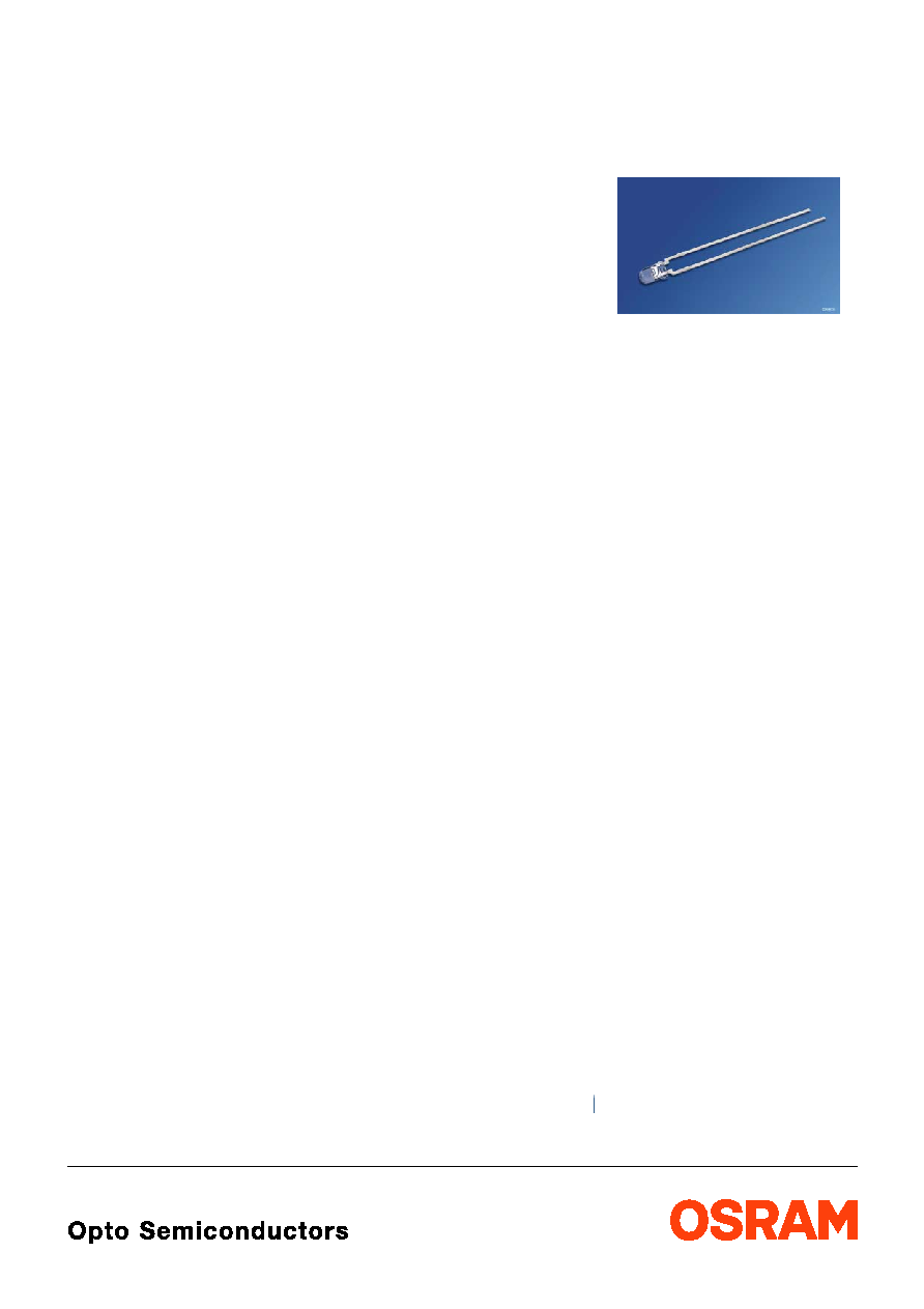
LW 3333
Hyper 3 mm (T1) LED, Non Diffused
Hyper-Bright LED
Vorl‰ufige Daten / Preliminary Data
2001-10-02
1
Besondere Merkmale
∑ Geh‰usetyp: nicht eingef‰rbtes, klares 3 mm
(T1) Geh‰use
∑ Besonderheit des Bauteils: enge
Abstrahlcharakteristik; Lˆtspieþe mit
Aufsetzebene
∑ Farbort: x= 0.32, y = 0.31 nach
CIE 1931 (weiþ)
∑ typ. Farbtemperatur: 6500 K
∑ Abstrahlwinkel: 40∞
∑ Technologie: InGaN
∑ optischer Wirkungsgrad: 6 lm/W
∑ Gruppierungsparameter: Lichtst‰rke, Farbort
∑ Lˆtmethode: Wellenlˆten (TTW)
∑ Verpackung: Sch¸ttgut, gegurtet lieferbar
∑ ESD-Festigkeit: ESD-sicher bis 2 kV nach
EOS/ESD-5.1-1993
Anwendungen
∑ Informationsanzeigen im Auþenbereich
∑ optischer Indikator
∑ Signal- und Symbolleuchten
∑ Markierungsbeleuchtung (z.B. Stufen,
Fluchtwege, u.‰.)
∑ Effektbeleuchtung (z.B. Sternenhimmel)
∑ Ersatz von Miniaturlampen
∑ Mˆbelbeleuchtung (z.B. Vitrinen)
Features
∑ package: colorless, clear 3 mm (T1) package
∑ feature of the device: narrow viewing angle,
solder leads with stand-off
∑ color coordinates: x = 0.32, y = 0.31 acc. to
CIE 1931 (white)
∑ typ. color temperature: 6500 K
∑ viewing angle: 40∞
∑ technology: InGaN
∑ optical efficiency: 6 lm/W
∑ grouping parameter: luminous intensity,
color coordinates
∑ soldering methods: TTW soldering
∑ packing: bulk, available taped on reel
∑ ESD-withstand voltage: up to 2 kV acc. to
EOS/ESD-5.1-1993
Applications
∑ outdoor displays
∑ optical indicators
∑ signal and symbol luminaire
∑ marker lights (e.g. steps, exit ways, etc.)
∑ lighting for special effects (e.g. starry sky)
∑ substitute for miniature flashlight
∑ furniture lighting (e.g. glass cupboards)
2001-10-02
2
LW 3333
Anm.: -1 Farbselektiert nach Farbortgruppen (siehe Seite 5)
Die Standardlieferform von Serientypen beinhaltet eine untere bzw. eine obere Familiengruppe
oder mindestens zwei Einzelgruppen.
In einer Verpackungseinheit / Gurt ist immer nur eine Helligkeitsgruppe enthalten.
Die technologiebedingte Helligkeits-Streuung der heutigen LED-Herstellprozesse ¸ber einen
l‰ngeren Fertigungszeitraum (Halbleitermaterial - Chipherstellung - Montageprozesss) erlaubt
keine Zusage einer einzelnen Helligkeitsgruppe. Daher m¸ssen mindestens zwei
Helligkeitsgruppen vorgesehen werden!
Note: -1 Color selection acc. to Chromaticity coordinate groups (see page 5)
The standard shipping format for serial types includes a lower or upper family group or at least
two individual groups.
No packing unit / tape ever contains more than one luminous intensity group.
Luminosity variations caused by the technology used in current LED manufacturing processes
over a protracted manufacturing period (semiconductor material - chip fabrication - assembly
process) mean that it is not possible to assign LEDs to a single luminous intensity group. For this
reason at least two luminous intensity groups must be provided!
Typ
Type
Emissions-
farbe
Color of
Emission
Geh‰usefarbe
Color of
Package
Lichtst‰rke
Luminous
Intensity
I
F
= 20 mA
I
V
(mcd)
Lichtstrom
Luminous
Flux
I
F
= 20 mA
V
(mlm)
Bestellnummer
Ordering Code
LW 3333-S2T2-1
LW 3333-T2V1-1
white
colorless clear
224 ... 450
355 ... 900
390 (typ.)
630 (typ.)
Q62703-Q5704
Q62703-Q5705
LW 3333
2001-10-02
3
Grenzwerte
Maximum Ratings
Bezeichnung
Parameter
Symbol
Symbol
Wert
Value
Einheit
Unit
Betriebstemperatur
Operating temperature range
T
op
≠ 40 ... + 100
∞C
Lagertemperatur
Storage temperature range
T
stg
≠ 40 ... + 100
∞C
Sperrschichttemperatur
Junction temperature
T
j
+ 100
∞C
Durchlassstrom
Forward current
I
F
20
mA
Stoþstrom
Surge current
t
10
µ
s,
D
= 0.005
I
FM
200
mA
Sperrspannung
Reverse voltage
V
R
5
V
Leistungsaufnahme
Power consumption
T
A
25 ∞C
P
tot
85
mW
W‰rmewiderstand
1)
Thermal resistance
Sperrschicht/Umgebung
Junction/ambient
Sperrschicht/Lˆtpad
Junction/solder point
Montage auf PC-Board FR 4 (Padgrˆþe
16 mm
2
)
mounted on PC board FR 4 (pad size
16 mm
2
)
Minimale Beinchenl‰nge
Minimum lead length
R
th JA
R
th JS
400
180
K/W
K/W
1)
R
th
erhˆht sich um 13 K/W pro mm Beinchenl‰nge.
Each additional 1 mm of lead length increases R
th
by 13 K/W.
2001-10-02
4
LW 3333
Kennwerte (
T
A
= 25 ∞C)
Characteristics
Bezeichnung
Parameter
Symbol
Symbol
Werte
Values
Einheit
Unit
Farbkoordinate x nach CIE 1931
1)
Chromaticity coordinate x acc. to CIE 1931
I
F
= 20 mA
x
0.32
≠
Farbkoordinate y nach CIE 1931
1)
Chromaticity coordinate y acc. to CIE 1931
I
F
= 20 mA
y
0.31
≠
Abstrahlwinkel bei 50 %
I
V
(Vollwinkel)
Viewing angle at 50 %
I
V
2
40
Grad
deg.
Durchlassspannung
2)
(typ.)
Forward voltage
(max.)
I
F
= 20 mA
V
F
V
F
3.5
4.1
V
V
Sperrstrom
(typ.)
Reverse current
(max.)
V
R
= 5 V
I
R
I
R
0.01
10
µ
A
µ
A
Temperaturkoeffizient von x
Temperature coefficient of x
I
F
= 20 mA; ≠10∞C
T
100∞C
TC
X
≠0.1
10
-3
/K
Temperaturkoeffizient von y
Temperature coefficient of y
I
F
= 20 mA; ≠10∞C
T
100∞C
TC
Y
≠0.2
10
-3
/K
Temperaturkoeffizient von
V
F
Temperature coefficient of
V
F
I
F
= 20 mA; ≠10∞C
T
100∞C
TC
V
≠3.0
mV/K
Optischer Wirkungsgrad
(typ.)
Optical efficiency
I
F
= 20 mA
opt
6
lm/W
1)
Farbortgruppen werden mit einer Stromeinpr‰gedauer von 25 ms und einer Genauigkeit von ±0,01 ermittelt.
Chromaticity coordinate groups are tested at a current pulse duration of 25 ms and a tolerance of ±0.01.
2)
Spannungswerte werden mit einer Stromeinpr‰gedauer von 1 ms und einer Genauigkeit von ±0,1 V ermittelt.
Voltages are tested at a current pulse duration of 1 ms and a tolerance of ±0.1 V.
LW 3333
2001-10-02
5
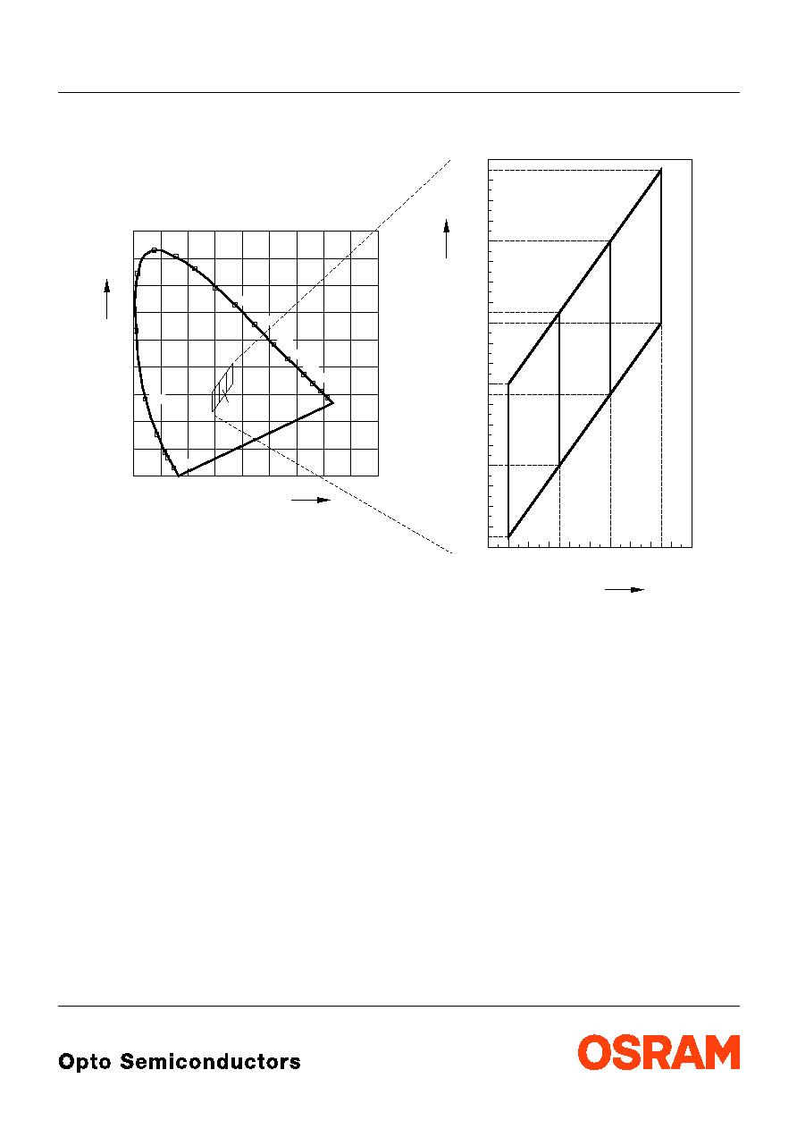
1)
Farbortgruppen
Chromaticity coordinate groups
OHA01327
520
530
540
550
560
570
580
590
600
610
620
630
0
0
0.1
0.2
0.3
0.4
0.5
0.6
0.7
0.8
0.9
0.1
0.2
0.3
0.4
0.5
0.6
0.7
0.8
0.9
510
500
490
480
470
450
460
0.28
0.23
0.24
0.30
0.32
0.34
0.36
0.25
0.26
0.27
0.28
0.29
0.30
0.31
0.32
0.33
0.34
0.35
0.36
0.37
0.38
0.39
0.40
0.42
0.38
+
+
group 3
group 4
group 5
E
0.29
0.31
0.33
0.35
Cy
0.41
Cx
Cy
0.37
Cx
2001-10-02
6
LW 3333
Helligkeitswerte werden mit einer Stromeinpr‰gedauer von 25 ms und einer Genauigkeit von
±
11% ermittelt.
Luminous intensity is tested at a current pulse duration of 25 ms and a tolerance of
±
11%
Helligkeits-Gruppierungsschema
Luminous Intensity Groups
Lichtgruppe
Luminous Intensity Group
Lichtst‰rke
Luminous Intensity
I
V
(mcd)
Lichtstrom
Luminous Flux
V
(mlm)
S2
T1
T2
U1
U2
V1
224 ... 280
280 ... 355
355 ... 450
450 ... 560
560 ... 710
710 ... 900
300 (typ.)
380 (typ.)
480 (typ.)
600 (typ.)
760 (typ.)
950 (typ.)
Gruppenbezeichnung auf Etikett
Group Name on Label
Beispiel: U2-3
Example: U2-3
Lichtgruppe
Luminous Intensity Group
Halbgruppe
Half Group
Farbortgruppe
Chromaticity coordinate group
U
2
3
LW 3333
2001-10-02
7
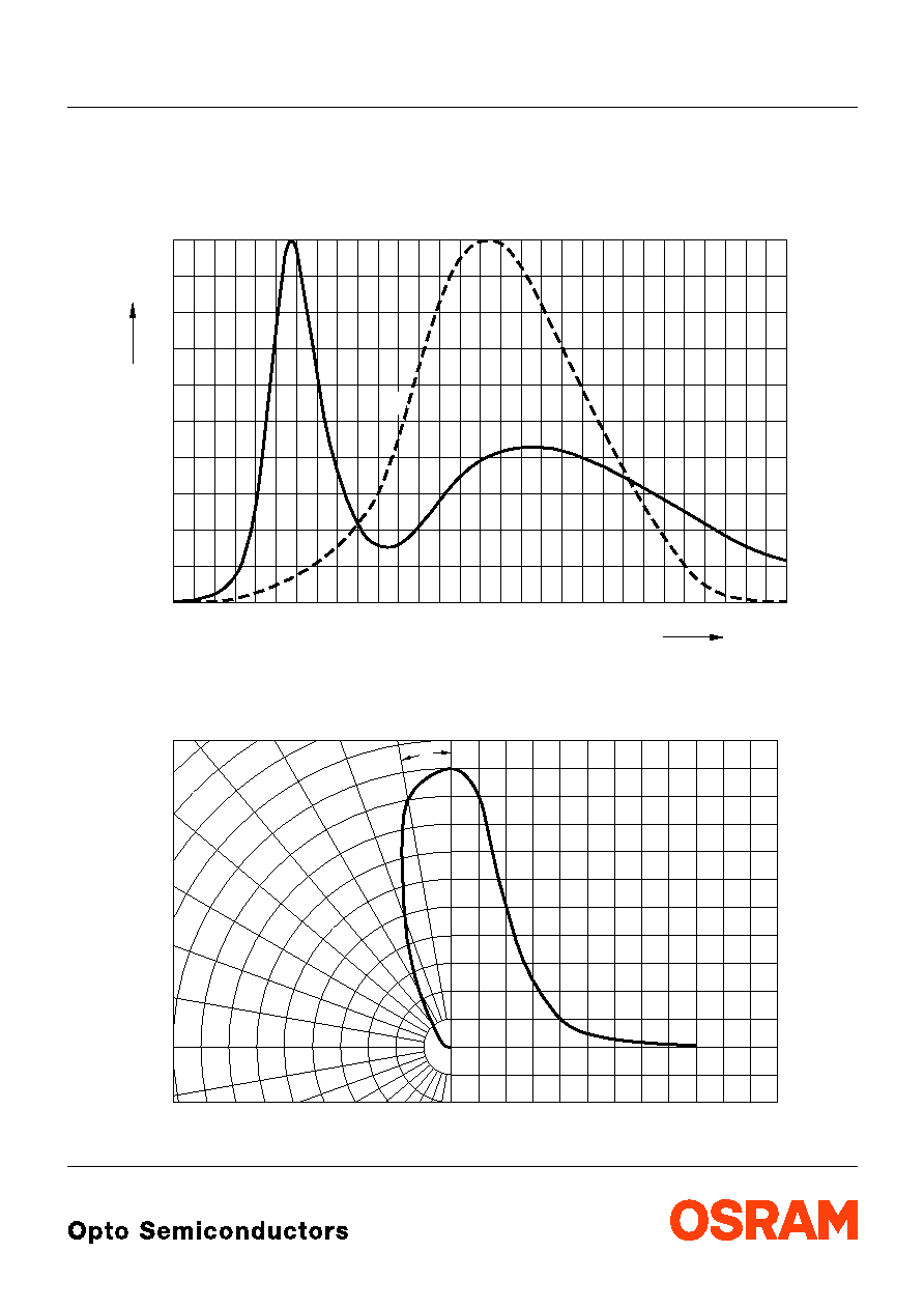
Relative spektrale Emission
I
rel
=
f
(
),
T
A
= 25 ∞C,
I
F
= 20 mA
Relative Spectral Emission
V(
) = spektrale Augenempfindlichkeit
Standard eye response curve
Abstrahlcharakteristik
I
rel
=
f
(
)
Radiation Characteristic
OHL00609
400
0
20
40
60
80
100
%
I
rel
nm
450
500
550
600
650
700
V
0
0.2
0.4
1.0
0.8
0.6
0∞
10∞
20∞
40∞
30∞
OHL01437
50∞
60∞
70∞
80∞
90∞
100∞
LW 3333
2001-10-02
8
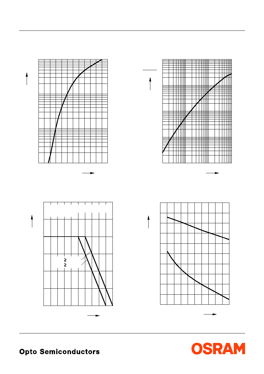
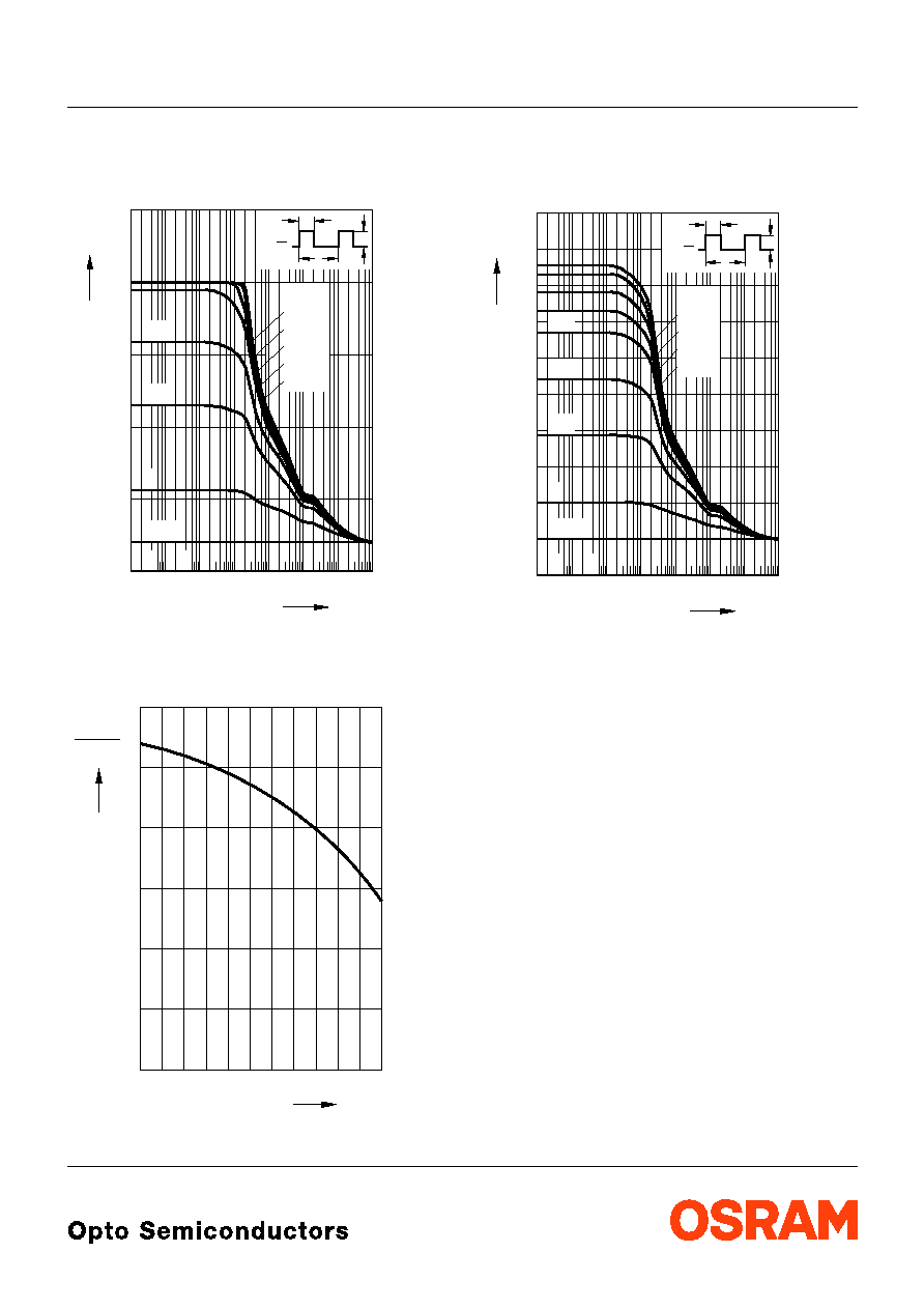
Durchlassstrom
I
F
=
f
(
V
F
)
Forward Current
T
A
= 25 ∞C
Maximal zul‰ssiger Durchlassstrom
Max. Permissible Forward Current
I
F
=
f
(
T
A
)
Relative Lichtst‰rke
I
V
/
I
V(20 mA)
=
f
(
I
F
)
Relative Luminous Intensity
T
A
= 25 ∞C
Farbortverschiebung
x, y =
f
(
I
F
)
Chromaticity Coordinate Shift
T
A
= 25 ∞C
OHL00611
10
-1
2.5
3
3.5
4
4.5 V 5
0
10
1
10
10
2
5
5
mA
5
2
I
F
V
F
OHL00044
0
I
F
T
0
mA
A
20
40
60
80 ∞C 100
Estimated average degradation
I
= -50%
V
5
10
15
20
25
30
MTTF
4000 h
MTTF
7000 h
V
V (20 mA)
10
-1
0
10
10
1
2
10
mA
10
-3
5
OHL00623
I
I
5
5
10
-2
10
-1
10
0
10
1
5
5
F
I
40
OHL00655
0.304
0
10
20
30
x, y
50
mA
0.306
0.308
0.310
0.312
0.314
0.316
0.318
0.324
x
y
F
I
LW 3333
2001-10-02
9
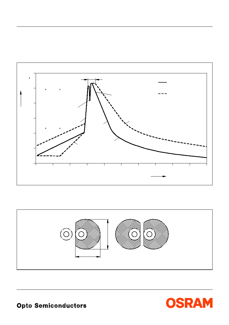
Zul‰ssige Impulsbelastbarkeit
I
F
=
f
(
t
p
)
Permissible Pulse Handling Capability
Duty cycle
D
= parameter,
T
A
= 25 ∞C
Relative Lichtst‰rke
I
V
/
I
V(25 ∞C)
=
f
(
T
A
)
Relative Luminous Intensity
I
F
= 20 mA
Zul‰ssige Impulsbelastbarkeit
I
F
=
f
(
t
p
)
Permissible Pulse Handling Capability
Duty cycle
D
= parameter,
T
A
= 85 ∞C
OHL00064
10
-5
D
=
0.005
0.01
0.02
0.05
0
I
F
t
0.1
p
-4
10
-3
10
-2
10
-1
10
0
10
1
10
2
10
s
A
0.05
0.10
0.15
0.20
0.25
0.033
0
0
1
0.5
0.2
t
D
=
T
P
t
F
I
T
P
OHL00870
0
-10
V
V (25 ∞C)
I
I
∞C
V
A
T
10
30
50
70
100
0.2
0.4
0.6
0.8
1.2
OHL00060
10
-5
D
=
0.005
0.01
0.02
0.05
0
I
F
t
p
-4
10
-3
10
-2
10
-1
10
0
10
1
10
2
10
0.01
0.02
0.03
0.04
0.05
0.06
0.07
0.08
0.10
s
A
0
0
0.033
1
0.5
0.2
0.1
D
T
t
=
P
t
T
P
I
F

2001-10-02
10
LW 3333
Maþzeichnung
Package Outlines
Maþe werden wie folgt angegeben: mm (inch) / Dimensions are specified as follows: mm (inch).
Kathodenkennung:
k¸rzerer Lˆtspieþ
Cathode mark:
short solder lead
Gewicht / Approx. weight: 0.15 g
0.4 (0.016)
0.6 (0.024)
3.1 (0.122)
3.4 (0.134)
Area not flat
5.7 (0.224)
6.1 (0.240)
¯
2.7 (0.106)
¯
2.9 (0.114)
4.8 (0.189)
4.4 (0.173)
3.7 (0.146)
3.5 (0.138)
27.0 (1.063)
29.0 (1.142)
0.8 (0.031)
0.4 (0.016)
0.4 (0.016)
0.7 (0.028)
1.2 (0.047)
1.8 (0.071)
GEXY6045
0.9 (0.035)
1.1 (0.043)
Cathode
spacing
2.54 (0.100)
0.6 (0.024)
0.4 (0.016)
LW 3333
2001-10-02
11
Lˆtbedingungen
Soldering Conditions
Wellenlˆten (TTW) (nach CECC 00802)
TTW Soldering (acc. to CECC 00802)
Empfohlenes Lˆtpaddesign
Wellenlˆten (TTW)
Recommended Solder Pad
TTW Soldering
Maþe werden wie folgt angegeben: mm (inch) / Dimensions are specified as follows: mm (inch).
OHLY0598
0
0
50
100
150
200
250
50
100
150
200
250
300
T
t
C
s
235 C
10 s
C
... 260
1. Welle
1. wave
2. Welle
2. wave
5 K/s
2 K/s
ca 200 K/s
C
C
... 130
100
2 K/s
Zwangsk¸hlung
forced cooling
Normalkurve
standard curve
Grenzkurven
limit curves
4 (0.157)
OHLPY985
4.8 (1.890)
2001-10-02
12
LW 3333
Published by OSRAM Opto Semiconductors GmbH & Co. OHG
Wernerwerkstrasse 2, D-93049 Regensburg
© All Rights Reserved.
Attention please!
The information describes the type of component and shall not be considered as assured characteristics.
Terms of delivery and rights to change design reserved. Due to technical requirements components may contain
dangerous substances. For information on the types in question please contact our Sales Organization.
If printed or downloaded, please find the latest version in the Internet.
Packing
Please use the recycling operators known to you. We can also help you ≠ get in touch with your nearest sales office.
By agreement we will take packing material back, if it is sorted. You must bear the costs of transport. For packing
material that is returned to us unsorted or which we are not obliged to accept, we shall have to invoice you for any costs
incurred.
Components used in life-support devices or systems must be expressly authorized for such purpose! Critical
components
1
may only be used in life-support devices or systems
2
with the express written approval of OSRAM OS.
1
A critical component is a component used in a life-support device or system whose failure can reasonably be expected
to cause the failure of that life-support device or system, or to affect its safety or the effectiveness of that device or
system.
2
Life support devices or systems are intended (a) to be implanted in the human body, or (b) to support and/or maintain
and sustain human life. If they fail, it is reasonable to assume that the health of the user may be endangered.
Revision History: 2001-10-02
Previous Version:
2001-03-01
Page
Subjects (major changes since last revision)
3
thermal resistance (footnote)
4
value (forward voltage)
Patent List
Patent No.
US 6 066 861, US 6 277 301