 | –≠–ª–µ–∫—Ç—Ä–æ–Ω–Ω—ã–π –∫–æ–º–ø–æ–Ω–µ–Ω—Ç: PD4437 | –°–∫–∞—á–∞—Ç—å:  PDF PDF  ZIP ZIP |

2001 OSRAM Opto Semiconductors Inc.∑ San Jose, CA
www.infineon.com/opto ∑ 408-456-4000
OSRAM Opto Semiconductors GmbH & Co. OHG ∑ Regensburg, Germany
www.osram-os.com ∑ +49-941-202-7178
1
July 5, 2001-14
HER
PD2435/PD3535/PD4435
RED
PD2436/PD3536/PD4436
BRIGHT GREEN
PD2437/PD3537/PD4437
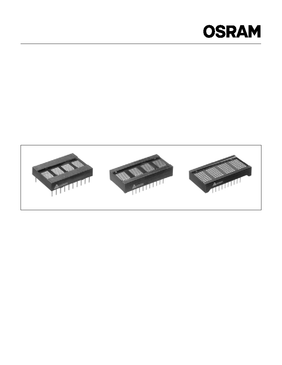
0.200" Character, PD2435/6/7
0.270" Character, PD3535/6/7
0.45" Character, PD4435/6/7
4-Character 5 x 7 Dot Matrix Alphanumeric
Programmable DisplayTM with
Built-in CMOS Control Functions
FEATURES
∑ Four Dot Matrix Characters in High Efficiency Red,
Red, and Bright Green
≠ PD2435/6/7, 0.200" High
≠ PD3535/6/7, 0.270" High
≠ PD4435/6/7, 0.45" High
∑ Built-in Memory, Decoders, Multiplexer and Drivers
∑ Wide Viewing Angle, X Axis ±55
∞
, Y Axis ±65
∞
∑ Categorized for Luminous Intensity
∑ 128 Character ASCII Format (Upper and Lower Case
Characters)
∑ 8 Bit Bidirectional Data BUS
∑ READ/WRITE Capability
∑ Dual In-Line Package Configuration, 0.600" Wide,
0.100" Pin Centers
∑ End-Stackable Package
PD243X
PD353X
PD443X
∑ Internal or External Clock
∑ Built-in Character Generator ROM
∑ TTL Compatible
∑ Easily Cascaded for Multidisplay Operation
∑ Less CPU Time Required
∑ Software Controlled Features:
≠ Programmable Highlight Attribute
(Blinking, Non-Blinking)
≠ Asynchronous Memory Clear Function
≠ Lamp Test
≠ Display Blank Function
≠ Single or Multiple Character Blinking Function
≠ Programmable Intensity
Three Brightness Levels
∑ Extended Operating Temperature Range:
≠ PD243X, PD353X: ≠40
∞
C to +85
∞
C
≠ PD443X: ≠40
∞
C to +70
∞
C

2001 OSRAM Opto Semiconductors Inc.∑ San Jose, CA
PD2535/6/7, PD3535/6/7, PD4435/6/7
www.infineon.com/opto ∑ 408-456-4000
OSRAM Opto Semiconductors GmbH & Co. OHG ∑ Regensburg, Germany
www.osram-os.com ∑ +49-941-202-7178
2
July 5, 2001-14
DESCRIPTION
These Programmable Displays are four digit display sys-
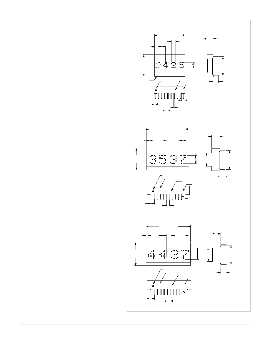
tem modules. The characters are 0.20" by 0.14"
(PD243X), 0.27" by 0.20" (PD353X), and 0.45" by 0.27"
(PD443X) 5 x 7 dot matrix arrays constructed with the
latest solid state technology in light emitting diodes.
Driving and controlling the LED arrays is a silicon gate
CMOS integrated circuit. This integrated circuit provides
all necessary LED drivers and complete multiplexing
control logic.
Additionally, the IC has the necessary ROM to decode
128 ASCII alphanumeric characters and enough RAM to
store the display's complete four digit ASCII message
with special attributes. These attributes, all software
programmable at the user's discretion, include a lamp
test, brightness control, displaying cursors, alternating
cursors and characters, and flashing cursors or charac-
ters.
The CMOS IC also incorporates special interface control
circuitry to allow the user to control the module as a fully
supported microprocessor peripheral. The module,
under internal or external clock control, has asynchro-
nous read, write, and memory clear over an eight bit par-
allel, TTL compatible, bi-directional data bus. Each
module is fully encapsulated within a package 1.0" x 0.7"
x 0.2" (PD253X), 1.4" x 0.72" x 0.285" (PD353X), and 1.5"
x 0.82" x 0.285" (PD443X). The standard 20 pin DIP con-
struction with two rows spaced at 0.6" on 0.1" centers is
wave solderable.
See the end of this data sheet or refer to Appnotes 18,
19, 22, and 23 for further details on handling and assem-
bling OSRAM Programmable Displays.
.700
(17.78)
Pin 1
location
.125
(3.18)
.200
(5.08)
PD243X
OSRAM YYWW Z
Luminous
Intensity Code
EIA date code
.160
±
.020
(4.06
±
.51)
.600
(15.24)
.200
(5.08)
Pin 1
Indicator
.050
(1.27)
.100 typ. (2.54)
.018 x .012 typ.
(.46 x .31)
1.000 max.
(25.40)
.140
(3.56)
.070
±
.004 typ.
(1.78
±
.10)
.250
(6.35)
at seating plane
and centered
on package
Tolerance: .XXX=0.02 (.51)
at seating plane
and centered
on package
PD3537
OSRAM YYWW Z
Luminous
Intensity
Code
.160
±
.020
(4.06
±
.51)
.600 typ.
(15.24)
.285
(7.24)
EIA date code
Pin 1 Identifier and ESD warning
.250
(6.35)
.100 (2.54) typ.
.018 x .012 typ.
(.46 x .31)
.720
max.
(18.29)
.175
(4.45)
1.400 max.
(35.56)
.350
(8.89)
typ.
.270 typ.
(6.86)
.200
(5.08)
typ.
.450
(11.43)
Part No.
Tolerance: .XXX=0.010 (.25)
unless max.
at seating plane
and centered
on package
PD4437
OSRAM YYWW Z
Luminous
Intensity Code
.160
±
.020
(4.06
±
.51)
.600 typ.
(15.24)
.285
(7.24)
EIA date code
Pin 1 Indicator
.300
(7.62)
.100 (2.54) typ.
.018 x .012
±
.002 typ.
(.46 x .31
±
.05)
.820
max.
(20.83)
.050
(1.27)
1.500 max.
(38.1)
.375
(9.53)
typ.
.45
±
.010
(11.43)
.270
(6.86)
typ.
.600
(15.24)
Part No.
Tolerance: .XXX=0.020 (.51)
Dimensions in Inches (mm)

2001 OSRAM Opto Semiconductors Inc.∑ San Jose, CA
PD2535/6/7, PD3535/6/7, PD4435/6/7
www.infineon.com/opto ∑ 408-456-4000
OSRAM Opto Semiconductors GmbH & Co. OHG ∑ Regensburg, Germany
www.osram-os.com ∑ +49-941-202-7178
3
July 5, 2001-14
Maximum Ratings
DC Supply Voltage.........................................≠0.5 V to +7.0 Vdc
Input Voltage Relative
to GND (all inputs)...............................≠0.5 V to
V
CC
+0.5 Vdc
Operating Temperature
PD243X/353X................................................. ≠40
∞
C to +85
∞
C
PD443X .......................................................... ≠40
∞
C to +70
∞
C
Storage Temperature....................................... ≠40
∞
C to +100
∞
C
Maximum Solder Temperature, .063" (1.59 mm)
below Seating Plane, t<5.0 s ........................................ 260
∞
C
Optical Characteristics at 25
∞
C
Spectral Peak Wavelength
HER ..................................................................... 635 nm typ.
Red ...................................................................... 660 nm typ.
Green ................................................................... 565 nm typ.
Viewing Angle
Horizontal
PD243X/353X .................................................................
±
55
∞
PD443X...........................................................................
±
40
∞
Vertical (off normal axis)..................................................
±
65
∞
Digit Height
PD243X........................................................ 0.200" (5.08 mm)
PD353X........................................................ 0.270" (6.86 mm)
PD443X........................................................ 0.45" (11.43 mm)
Time Averaged Luminous Intensity
(1)
Red ...............................................................30
µ
cd/LED min.
HER/Green....................................................90
µ
cd/LED min.
LED to LED Intensity Matching...............................1.8:1.0 max.
Device to Device (one bin) ......................................1.5:1.0 max.
Bin to Bin (adjacent bins).........................................1.9:1.0 max.
Note:
1)
Peak luminous intensity values can be calculated by
multiplying these values by 7.
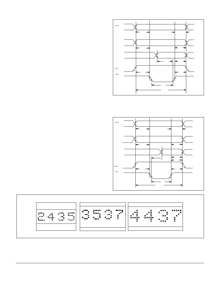
Figure 2. Timing Characteristics--Data "Write" Cycle
Notes:
1. All input voltages are
V
IL
=0.8 V,
V
IH
=2.0 V.
2. These waveforms are not edge triggered.
Figure 3. Timing Characteristics--Data "Read" Cycle
TDS
TDH
TW
TACC
TAH
TAS
TCEH
TCES
2.0 V
0.8 V
CE0, CE1
A0, A1
RD
2.0 V
0.8 V
2.0 V
0.8 V
2.0 V
0.8 V
D0≠D6
2.0 V
0.8 V
TRS
TRH
WR
*
*
*
*
*
T
DD
T
R
T
AH
T
AS
T
CEH
T
CES
2.0 V
0.8 V
CE0, CE1
A0≠A3
T
RACC
2.0 V
0.8 V
2.0 V
0.8 V
2.0 V
0.8 V
D0≠D6
2.0 V
0.8 V
T
WS
T
WH
WR
RD
T
DH
T
RI
*
*
*
*
DATA OUT
*
Figure 1. Top View
DIGIT3 DIGIT2 DIGIT1 DIGIT0
DIGIT3
DIGIT2
DIGIT1
DIGIT0
DIGIT3
DIGIT2
DIGIT1
DIGIT0
20 11
20 11
20 11
1 10 1 10 1 10

2001 OSRAM Opto Semiconductors Inc.∑ San Jose, CA
PD2535/6/7, PD3535/6/7, PD4435/6/7
www.infineon.com/opto ∑ 408-456-4000
OSRAM Opto Semiconductors GmbH & Co. OHG ∑ Regensburg, Germany
www.osram-os.com ∑ +49-941-202-7178
4
July 5, 2001-14
Switching Specifications
(
V
CC
=4.5 V)
Switching Specifications
(
V
CC
=4.5 V)
Notes:
1)
Wait 1.0
µ
s between any Reads or Writes after writing a Control Word with a Clear (D7=1). Wait 1.0
µ
s
between any Reads or Writes after Clearing a Control Word with a Clear (D7=0). All other Reads and
Writes can be back to back.
2)
All input voltages are (
V
IL
=0.8 V,
V
IH
=2.0 V)
3)
Data out voltages are measured with 100 pF on the data bus and the ability to source = ≠40
µ
A and
sink=1.6 mA The rise and fall times are 60 ns.
V
OL
=0.4 V,
V
OH
=2.4 V.
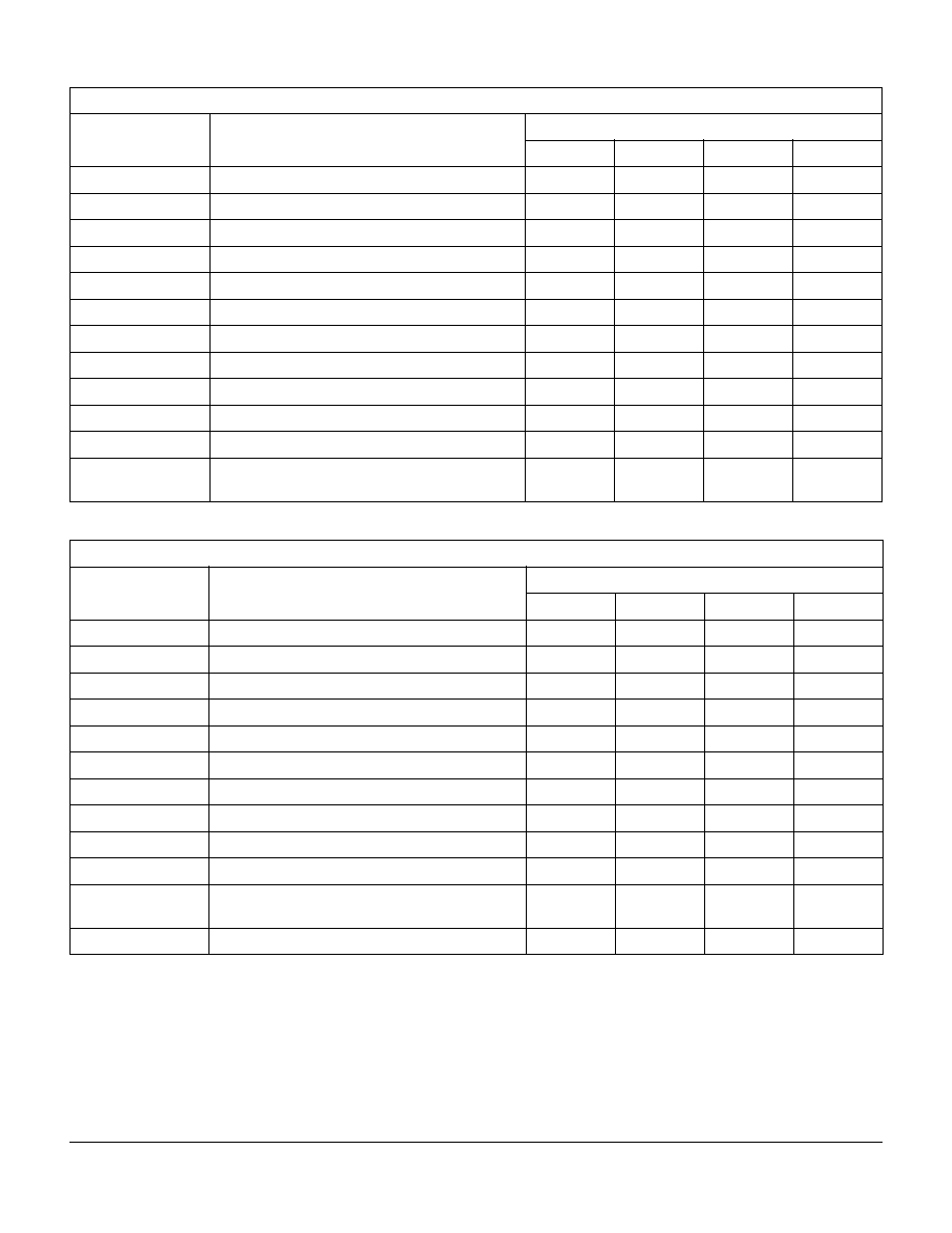
Write Cycle Timing
Parameter
Description
Specification Minimum
≠40
∞
C
25
∞
C
85
∞
C
Units
T
CLR
(1)
Clear
RAM
1.0
1.0
1.0
µ
s
T
CLRD
(1)
Clear RAM Disable
1.0
1.0
1.0
µ
s
T
AS
Address Setup
10
10
10
ns
T
CES
Chip Enable Setup
0
0
0
ns
T
RS
Read Enable Setup
10
10
10
ns
T
DS
Data Setup
20
30
50
ns
T
W
Write Pulse
60
70
90
ns
T
AH
Address
Hold
20
30
40
ns
T
DH
Data Hold
20
30
40
ns
T
CEH
Chip Enable Hold
0
0
0
ns
T
RH
Read Enable Hold
20
30
40
ns
T
ACC
Total Access Time = Setup Time + Write
Time + Hold Time
90
110
140
ns
Read Cycle Timing
Parameter
Description
Specification Minimum
≠40
∞
C
25
∞
C
85
∞
C
Units
T
AS
Address
Setup
0
0
0
ns
T
CES
Chip Enable
0
0
0
ns
T
WS
Write Enable Setup
20
30
40
ns
T
DD
Data Delay Time
100
150
175
ns
T
R
Read Pulse
150
175
200
ns
T
AH
Address
Hold
0
0
0
ns
T
DH
Data Hold
0
0
0
ns
T
TRI
Time to Tristate (Max. time)
30
40
50
ns
T
CEH
Chip Enable Hold
0
0
0
ns
T
WH
Write Enable Hold
30
40
50
ns
T
ACC
Total Access Time = Setup Time + Read
Time + Time to Tristate
200
245
290
ns
T
WAIT
(1)
Wait Time between Reads
0
0
0
ns

2001 OSRAM Opto Semiconductors Inc.∑ San Jose, CA
PD2535/6/7, PD3535/6/7, PD4435/6/7
www.infineon.com/opto ∑ 408-456-4000
OSRAM Opto Semiconductors GmbH & Co. OHG ∑ Regensburg, Germany
www.osram-os.com ∑ +49-941-202-7178
5
July 5, 2001-14
DC Characteristics
at 25
∞
C
Note:
1)
D0 to D7 have no pull-up resistors so current is negligible.
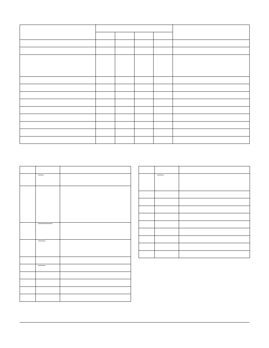
Pin Assignments and Definitions
Parameter
Limits
Conditions
Min.
Typ.
Max.
Units
V
CC
4.5
5.0
5.5
Volts
Nominal
I
CC
(Blank)
--
2.5
3.5
mA
V
CC
=5.0 V, A2=1, all other inputs low.
I
CC
80 LEDs/unit (100% Bright)
PD243X
PD353X
PD443X
--
115
145
150
130
165
170
mA
mA
mA
V
CC
=5.0 V
V
CC
=5.0 V
V
CC
=5.0 V
V
IL
--
--
0.8
Volts
V
CC
=4.5 V to 5.5 V
V
IH
2.0
--
--
Volts
V
CC
=4.5 V to 5.5 V
I
IL
(except D0 to D7)
(1)
25
--
100
µ
A
V
CC
=4.5 V to 5.5 V, V
IN
=0.8 V
V
OL
--
--
0.4
Volts
V
CC
=4.5 V to 5.5 V
V
OH
2.4
--
--
Volts
V
CC
=4.5 V to 5.5 V
I
OH
≠8.9
--
--
mA
V
CC
=4.5 V, V
OH
=2.4 V
I
OL
1.6
--
--
mA
V
CC
=4.5 V, V
OL
=0.4 V
Data I/O Bus Loading
--
--
100
pF
--
Clock I/O Bus Loading
--
--
240
pF
--
Pin
Function
Definition
1
RD
Active low, will enable a processor to
read all registers in the display.
2
CLK I/O
If CLK SEL (pin 3) is low, then expect
an external clock source into this pin.
If CLK SEL is high, then this pin will
be the master or source into this pin.
If CLK SEL is high, then this pin will
be the master or source for all other
devices which have CLK SEL low.
3
CLKSEL
CLOCK SELECT determines the
action of pin 2. CLK I/O, see the sec-
tion on Cascading for an example.
4
RST
Reset. Used to synchronize blinking.
Will not clear the display. The reset
pulse should be less than 1 ms
5
CE1
Chip enable (active high).
6
CE0
Chip enable (active low).
7
A2
Address input (MSB).
8
A1
Address input.
9
A0
Address input (LSB).
10
GND
Ground.
Pin Assignments and Definitions (continued)
Pin
Function
Definition
11
WR
Write. Active low. If the device is
selected, a low on the write input
loads the data into memory.
12
D7
Data Bus bit 7 (MSB).
13
D6
Data Bus bit 6.
14
D5
Data Bus bit 5.
15
D4
Data Bus bit 4.
16
D3
Data Bus bit 3.
17
D2
Data Bus bit 2.
18
D1
Data Bus bit 1.
19
D0
Data Bus bit 0 (LSB).
20
V
CC
Positive power pin.

2001 OSRAM Opto Semiconductors Inc.∑ San Jose, CA
PD2535/6/7, PD3535/6/7, PD4435/6/7
www.infineon.com/opto ∑ 408-456-4000
OSRAM Opto Semiconductors GmbH & Co. OHG ∑ Regensburg, Germany
www.osram-os.com ∑ +49-941-202-7178
6
July 5, 2001-14
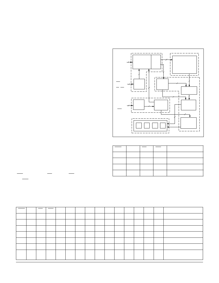
Functional Description
The block diagram includes 5 major blocks and internal regis-
ters (indicated by dotted lines).
Display Memory consists of a 5 x 8 bit RAM block. Each of
the four 8-bit words holds 7-bits of ASCII data (bits D0≠D6)
and an attribute select bit (Bit D6). The fifth 8-bit memory
word is used as a control word register. A detailed description
of the control register and its functions can be found in the
Control Word section. Each 8-bit word is addressable and can
be read from or written to.
The Control Logic dictates all of the features of the display
device and is discussed in the Control Word section of this
data sheet.
The Character Generator converts the 7-bit ASCII data into
the proper dot pattern for the 128 characters shown in the
character set chart.
The Clock Source can originate either from the internal oscilla-
tor clock or from an external source--usually from the output of
another display in a multiple module array.
The Display Multiplexer controls all display output to the digit
drivers so no additional logic is required for a display system.
The Column Drivers are connected directly to the display.
The Display has four digits. Each of the four digits is com-
prised of 35 LEDs in a 5 x 7 dot array which makes up the
alphanumeric characters.
The intensity of the display can be varied by the Control Word
in steps of 0% (Blank), 25%, 50%, and full brightness.
The Reset pin when activated clears the internal counter. A reset
is usually done after power up and is of very short duration-nano-
seconds or microseconds. If the reset pin is held low for a longer
time (milliseconds) some or all LEDs in the bottom row may light
up. The appearance of lit LEDs during a "reset" is not an indica-
tion of a malfunctioning part. It is advisable to keep the reset
pulse as short as possible to avoid displaying a row of lit LEDs.
Microprocessor Interface
The interface to the microprocessor is through the address
lines. (A0≠A2), the data bus (D0≠D7), two chip select lines
(CE0, CE1), and read (RD) and write (WR) lines.
The CE0 should be held low when executing a read, or write
operation. CE1 must be held high.
The read and write lines are both active low. During a valid read
the data input lines (D0≠D7) become outputs. A valid write will
enable the data as input lines.
Data Input Commands
CEO
CE1
RD
WR
A2
A1
A0
D7
D6
D5
D4
D3
D2
D1
D0
Operation
1
0
X
X
X
X
X
X
X
X
X
X
X
X
X
No Change
0
1
0
1
1
0
0
X
X
X
X
X
X
X
X
Read Digit 0 Data to Bus
0
1
1
0
1
0
0
0
0
1
0
0
1
0
0
($) Written to Digit 0
0
1
1
0
1
0
1
0
1
0
1
0
1
1
1
(W) Written to Digit 1
0
1
1
0
1
1
0
0
1
1
0
0
1
1
0
(f) Written to Digit 2
0
1
1
0
1
1
1
0
0
1
1
0
0
1
1
(3) Written to Digit 3
0
1
1
0
1
0
0
1
X
X
X
X
X
X
X
Char. Written to Digit 0
and Cursor Enabled
Input Buffering
If a cable length of 6 inches or more is used, all inputs to the
display should be buffered with a tri-state non-inverting buffer
mounted as close to the display as conveniently possible. Rec-
ommended buffers are: 74LS245 for the data lines and
74LS244 for the control lines.
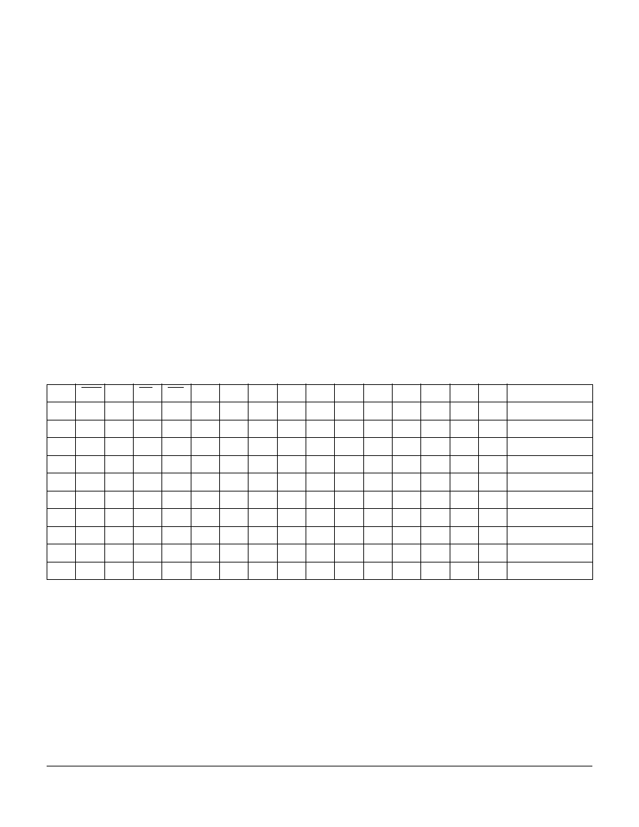
Figure 4. Block Diagram
Figure 5. Mode Selection
0=Low logic level, 1=High logic level, X=Don't care
CEO
CE1
RD
WR
Operation
0
1
0
0
None
1
X
X
X
None
X
0
X
X
None
X
X
1
1
None
Display Memory
(RAM) 4x8
Output
Control
Logic
Control
Reg
1x8
128 Char
ROM
128 x 5
Decode
and
Mux
Output
Latch
OSC
Logic
Display
Multiplexer
Column
Drivers
Row
Drivers
Display
D0-D7
CE0,CE1
A0-A2
RD, WR
CLK SEL
XCLK
RST
20
3
3
5
8
14
1
15
1
7
3
20
4
8

2001 OSRAM Opto Semiconductors Inc.∑ San Jose, CA
PD2535/6/7, PD3535/6/7, PD4435/6/7
www.infineon.com/opto ∑ 408-456-4000
OSRAM Opto Semiconductors GmbH & Co. OHG ∑ Regensburg, Germany
www.osram-os.com ∑ +49-941-202-7178
7
July 5, 2001-14
There are five registers within the display. Four of these regis-
ters are used to hold the ASCII/attribute code of the four dis-
play characters. The fifth register is the Control Word, which is
used to blink, blank, clear, or dim the entire display, or to
change the presentation (attributes) of individual characters.
Addressing
The addresses within the display device are shown below. Digit
0 is the rightmost digit of the display, while digit 3 is on the left.
Although there is only one Control Word, it is duplicated at the
four address locations 0≠3. Data can be read from any of these
locations. When one of these locations is written to, all of them
will change together.
Bit D7 of any of the display digit locations is used to allow an
attribute to be assigned to that digit. The attributes are dis-
cussed in the next section. If Bit D7 is set to a one, that charac-
ter will be displayed using the attribute. If bit D7 is cleared, the
character will display normally.
Address
Contents
A2
A1
A0
0
X
X
Control Word
1
0
0
Digit 0 (rightmost)
1
0
1
Digit 1
1
1
0
Digit 2
1
1
1
Digit 3 (leftmost)
Control Word
When address bit A2 is taken low, the Control Word is
accessed. The same Control Word appears in all four of the
lower address spaces of the display. Through the Control Word,
the display can be cleared, the lamps can be tested, display
brightness can be selected, and attributes can be set for any
characters which have been loaded with their most significant
bit (D7) set high.
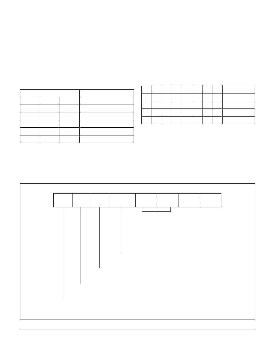
Brightness (D0, D1): The state of the lower two bits of the
Control Word are used to set the brightness of the entire dis-
play, from 0% to 100%. The table below shows the correspon-
dence of these bits to the brightness.
X=don't care
Attributes (D2≠D4): Bits D2, D3, and D4 control the visual
attributes (i.e., blinking) of those display digits which have been
written with bit D7 set high. In order to use any of the four
attributes, the Cursor Enable bit (D4 in the Control Word) must
be set. When the Cursor Enable bit is set, and bit D7 in a char-
acter location is set, the character will take on one of the fol-
lowing display attributes.
D7
D6
D5
D4
D3
D2
D1
D0
Operation
0
0
X
X
X
X
0
0
Blank
0
0
X
X
X
X
0
1
25% brightness
0
0
X
X
X
X
1
0
50% brightness
0
0
X
X
X
X
1
1
Full brightness
Control Word Format
D7 D6 D5 D4 D3 D2 D1 D0
Clear
Blink
Attributes
Brightness
Lamp
test
Attribute
enable
D7 Clear
0 Standard Operation
1 Clear Entire Display
D6 Lamp test
0 Standard Operation
1 Display All Dots at 50% Brightness
D5 Blink
0 Blink Attribute Disabled
1 Blink Entire Display
D4 Attribute enable
0 Disable above Attributes
1 Enable above Attributes
D3 D2 Attributes
0 0 Display Cursor instead
of Character
0 1 Blink Character
1 0 Display Blinking Cursor
instead of Character
1 1 Alternate Character
with Cursor
D1 D0 Brightness
0 0 0% (blank)
0 1 25%
1 0 50%
1 1 100%

2001 OSRAM Opto Semiconductors Inc.∑ San Jose, CA
PD2535/6/7, PD3535/6/7, PD4435/6/7
www.infineon.com/opto ∑ 408-456-4000
OSRAM Opto Semiconductors GmbH & Co. OHG ∑ Regensburg, Germany
www.osram-os.com ∑ +49-941-202-7178
8
July 5, 2001-14
*"Cursor"= all dots in a single character space lit to half brightness
X=Don't care
B=Depends on the selected brightness.
Attributes are non-destructive. If a character with bit D7 set is
replaced by a cursor (Control Word bit D4 is set, and D3=D2=0)
the character will remain in memory and can be revealed again
by clearing D4 in the Control Word.
Blink (D5): The entire display can be caused to blink at a rate of
approximately 2.0 Hz by setting bit D5 in the Control Word. This
blinking is independent of the state of D7 in all character locations.
To synchronize the blink rate in a bank of these devices, it is
necessary to tie all devices' clocks and resets together as
described in a later section of this data sheet.
D7
D6
D5
D4
D3
D2
D1
D0
Operation
0
0
0
0
X
X
B
B
Disable highlight
attribute
0
0
0
1
0
0
B
B
Display cursor*
instead of
character
0
0
0
1
0
1
B
B
Blink single
character
0
0
0
1
1
0
B
B
Display blinking
cursor* instead
of character
0
0
0
1
1
1
B
B
Alternate charac-
ter with cursor*
Lamp Test (D6): When the Lamp Test bit is set, all dots in the
entire display are lit at half brightness. When this bit is cleared,
the display returns to the characters that were showing before
the lamp test.
Clear Data (D7): When D7 is set (D7=1) in the Control Word, all
(display) memory bits are reset to zero and the display goes blank.
A second control word must be written into the chip with D7
reset (D7=0) to set up attributes and brightness levels.
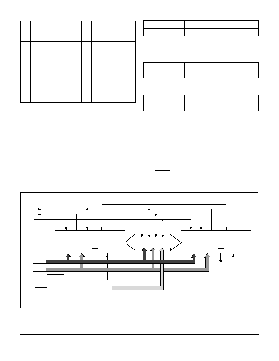
The SMC-4740 oscillator is designed to drive up to 16 displays
with input loading of 15 pF each.
The general requirements for cascading 16 displays are:
1. Determine the correct address for each display.
2. Tie CE0 to ground and use CE1 from an address.
3. Select one of the displays to provide the clock for the
other displays.
4. Tie CLKSEL to ground on other displays.
5. Use RST to synchronize the blinking between the displays.
D7
D6
D5
D4
D3
D2
D1
D0
Operation
0
0
1
X
X
X
B
B
Blinking display
D7
D6
D5
D4
D3
D2
D1
D0
Operation
0
1
0
X
X
X
X
X
Lamp test
D7
D6
D5
D4
D3
D2
D1
D0
Operation
1
0
X
X
X
X
X
X
Clear
Figure 6. Cascading Diagram
WR RD RST CLK I/O CLKSEL
D0-D7 A0-A2 CE0 CE1
Programmable Display
WR RD RST CLK I/O CLKSEL
D0-D7 A0-A2 CE0 CE1
Programmable Display
14 More Displays
in between
Address Decode Chip 1 to 14
Address
Data I/O
RST
RD
WR
V
CC
A4
A5
A6
Address
Decoder

2001 OSRAM Opto Semiconductors Inc.∑ San Jose, CA
PD2535/6/7, PD3535/6/7, PD4435/6/7
www.infineon.com/opto ∑ 408-456-4000
OSRAM Opto Semiconductors GmbH & Co. OHG ∑ Regensburg, Germany
www.osram-os.com ∑ +49-941-202-7178
9
July 5, 2001-14
How to Load Information Into the Display
Information loaded into the display can be either ASCII data or
Control Word data. The following procedure (see also Typical
Loading Sequence) will demonstrate a typical loading sequence
and the resulting visual display. The word STOP is used in all of
the following examples.
Set Brightness
Step 1
Set the brightness level of the entire display to your
preference (example: 100%)
Load Four Characters
Step 2
Load an "S" in the left hand digit.
Step 3
Load a "T" in the next digit.
Step 4
Load an "O" in the next digit.
Step 5
Load a "P" in the right hand digit.
If you loaded the information correctly, the display
now should show the word "STOP."
Blink a Single Character
Step 6
Into the digit, second from the right, load the hex
code "CF," which is the code for an "O" with the
D7 bit added as a control bit.
Note:
The "O" is the only digit which has the control bit (D7)
added to normal ASCII data.
Typical Loading Sequence
* Blinking character
Character alternating with cursor (all dots lit)
CEO
CE1
RD
WR
A2
A1
A0
D7
D6
D5
D4
D3
D2
D1
D0
Display
1.
L
H
H
L
L
X
X
0
0
0
0
0
0
1
1
2.
L
H
H
L
H
H
H
0
1
0
1
0
0
1
1
S
3.
L
H
H
L
H
H
L
0
1
0
1
0
1
0
0
ST
4.
L
H
H
L
H
L
H
0
1
0
0
1
1
1
1
STO
5.
L
H
H
L
H
L
L
0
1
0
1
0
0
0
0
STOP
6.
L
H
H
L
H
L
H
1
1
0
0
1
1
1
1
STOP
7.
L
H
H
L
L
X
X
0
0
0
1
0
1
1
1
STO*P
8.
L
H
H
L
H
H
H
1
1
0
1
0
0
1
1
S*TO*P
9.
L
H
H
L
L
X
X
0
0
0
1
1
1
1
1
STOP
10.
L
H
H
L
L
X
X
0
0
1
0
0
0
1
1
S*T*O*P*
Step 7
Load enable blinking character into the control
word register. The display should show "STOP"
with a flashing "O".
Add Another Blinking Character
Step 8
Into the left hand digit, load the hex code "D3"
which gives an "S" with the D7 bit added as a
control bit. The display should show "STOP"
with flashing "O" and a flashing "S."
Alternate Character/Cursor Enable
Step 9
Load enable alternate character/cursor into the
control word register. The display now should show
"STOP" with the "O" and the "S" alternating
between the letter and cursor (all dots lit).
Initiate Four Character Blinking
(Regardless of Control Bit setting)
Step 10
Load enable display blinking. The display now
should show the entire word "STOP" blinking.

2001 OSRAM Opto Semiconductors Inc.∑ San Jose, CA
PD2535/6/7, PD3535/6/7, PD4435/6/7
www.infineon.com/opto ∑ 408-456-4000
OSRAM Opto Semiconductors GmbH & Co. OHG ∑ Regensburg, Germany
www.osram-os.com ∑ +49-941-202-7178
10
July 5, 2001-14
Electrical and Mechanical Considerations
The CMOS IC of the display is designed to provide resistance
to both Electrostatic Discharge Damage and Latch Up due to
voltage or current surges. Several precautions are strongly rec-
ommended to avoid overstressing these built-in safeguards.
ESD Protection
Display users should be careful to handle the devices consis-
tent with Standard ESD protection procedures. Operators
should wear appropriate wrist, ankle or feet ground straps and
avoid clothing that collects static charges. Work surfaces, tools
and transport carriers that come into contact with unshielded
devices or assemblies should also be appropriately grounded.
Latch up Protection
Latch up is a condition that occurs in CMOS ICs after the input
protection diodes have been broken down. These diodes can
be reversed through several means:
V
IN
<GND, V
IN
>V
CC
+
0.5 V, or through excessive currents
forced on the inputs. When these situations exist, the IC may
develop the response of an SCR and begin conducting as much
as one amp through the V
CC
pin. This destructive condition will
persist (latched) until device failure or the device is turned off.
The Voltage Transient Suppression Techniques and buffer inter-
faces for longer cable runs help considerably to prevent latch
conditions from occurring. Additionally, the following Power Up
and Power Down sequence should be observed.
Power up Sequence
1. Float all active signals by tri-stating inputs to displays.
2. Apply V
CC
and GND to the display.
3. Apply active signals to the displays by enabling all input
signals per application.
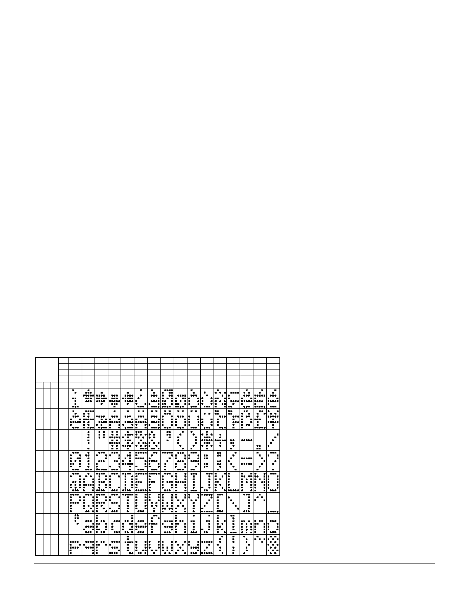
Figure 7. Character Set
ASCII
CODE
D0
D1
D2
D3
0
0
0
0
0
1
0
0
0
1
0
1
0
0
2
1
1
0
0
3
0
0
1
0
4
1
0
1
0
5
0
1
1
0
6
1
1
1
0
7
0
0
0
1
8
1
0
0
1
9
0
1
0
1
A
1
1
0
1
B
0
0
1
1
C
1
0
1
1
D
0
1
1
1
E
1
1
1
1
F
0
0
0
0
1
1
1
1
0
0
1
1
0
0
1
1
0
1
0
1
0
1
0
1
0
1
2
3
4
5
6
7
D6 D5 D4 HEX
Notes:
1. A2 must be held high for ASCII data.
2. Bit D7=1 enables attributes for the
assigned digit.
Power Down Sequence
1. Float all active signals by tri-stating the inputs to the display.
2. Turn off the power to the display.
Soldering Considerations
These displays can be hand soldered with SN63 solder using a
grounded iron set to 260
∞
C.
Wave soldering is also possible following these conditions: Pre-
heat that does not exceed 93
∞
C on the solder side of the PC
board or a package surface temperature of 85
∞
C. Water soluble
organic acid flux (except carboxylic acid) or rosin-based RMA
flux without alcohol can be used.
Wave temperature is 245
∞
C
±
5
∞
C with a dwell between 1.5
seconds to 3.0 seconds. Exposure to the wave should not
exceed temperatures above 260
∞
C, for 5 seconds at 0.063"
below the seating plane. The packages should not be
immersed in the wave.
Voltage Transient Suppression
It has become common practice to provide 0.01
µ
F bypass
capacitors liberally in digital systems. Like other CMOS cir-
cuitry, the Intelligent Display controller chip has very low
power consumption and the usual 0.01
µ
F would be adequate
were it not for the LEDs. To prevent power supply transients,
capacitors with low inductance and high capacitance at high
frequencies are required. This suggests a solid tantalum or
ceramic disc for high frequency bypass. For multiple display
module systems distribute the bypass capacitors evenly, keep-
ing capacitors as close to the power pins as possible. Use a
0.01
µ
F capacitor for each display module and a 22
µ
F for
every third display module.

2001 OSRAM Opto Semiconductors Inc.∑ San Jose, CA
PD2535/6/7, PD3535/6/7, PD4435/6/7
www.infineon.com/opto ∑ 408-456-4000
OSRAM Opto Semiconductors GmbH & Co. OHG ∑ Regensburg, Germany
www.osram-os.com ∑ +49-941-202-7178
11
July 5, 2001-14
Incandescent (with almost no green) or fluorescent (with
almost no red) lights do not have the flat spectral response of
sunlight. Plastic band-pass filters are inexpensive and effective
in optimizing contrast ratios. The PD2435/3535/4435 is high
efficiency red display and should be matched with a long
wavelength pass filter in the 570 nm to 590 nm range. The
PD2436/3536/4436 is a standard red display and should be
matched with a long wavelength pass filter in the 600 nm to
620 nm range. The PD2437/3537/4437 should be matched
with a yellow-green band-pass filter that peaks at 565 nm. For
displays of multiple colors, neutral density grey filters offer the
best compromise.
Additional contrast enhancement can be gained through shad-
ing the displays. Plastic band-pass filters with built-in louvers
offer the "next step up" in contrast improvement. Plastic filters
can be further improved with anti-reflective coatings to reduce
glare. The trade-off is "fuzzy" characters. Mounting the filters
close to the display reduces this effect. Care should be taken
not to overheat the plastic filters by allowing for proper air flow.
Optimal filter enhancements for any condition can be gained
through the use of circular polarized, anti-reflective, band-pass
filters. The circular polarizing further enhances contrast by
reducing the light that travels through the filter and reflects back
off the display to less than 1%. Proper intensity selection of the
displays will allow 10,000 foot candle sunlight viewability.
Several filter manufacturers supply quality filter materials.
Some of them are: Panelgraphic Corporation, W. Caldwell, NJ;
SGL Homalite, Wilmington, DE; 3M Company, Visual Products
Division, St. Paul, MN; Polaroid Corporation, Polarizer Division,
Cambridge, MA; Marks Polarized Corporation, Deer Park, NY;
Hoya Optics, Inc., Fremont, CA.
One last note on mounting filters: recessing display and bezel
assemblies is an inexpensive way to provide a shading effect in
overhead lighting situations. Several Bezel manufacturers are:
R.M.F. Products, Batavia, IL; Nobex Components, Griffith Plas-
tic Corp., Burlingame, CA; Photo Chemical Products of Califor-
nia, Santa Monica, CA; I.E.E.Atlas, Van Nuys, CA.
See Appnote 23.
Post Solder Cleaning Procedures
The least offensive cleaning solution is hot D.l. water (60
∞
C) for
less than 15 minutes. Addition of mild saponifiers is acceptable.
Do not use commercial dishwasher detergents.
For faster cleaning, solvents may be used. Carefully choose the
solvents as some may chemically attack the package. Maxi-
mum exposure should not exceed two minutes at elevated
temperatures. Acceptable solvents are: TF (trichlorotrifluoroet-
hane), TA, 111 Trichloroethane, and unheated acetone.
(1)
Note:
1)
Acceptable commercial solvents are: Basic TF Arklone P.
Genesolv D, Genesolv DA, BlacoTron TF, Blaco-Tron TA and,
Freon TA.
Do not use solvents containing alcohol, methanol, methylene
chloride, ethanol, TP35, TCM, TMC, TMS+, TE, and TES. Since
many commercial mixtures exist, you should contact your pre-
ferred solvent vendor for chemical composition information.
Some major solvent manufacturers are: Allied Chemical Corpo-
ration, Specialty Chemical Division, Morristown, NJ; Baron-
Blakeslee, Chicago, IL; Dow Chemical, Midland, Ml; E.l. DuPont
de Nemours & Co., Wilmington, DE.
For further information refer to Appnotes 18 and 19.
An alternative to soldering and cleaning the display modules is
to use sockets. Naturally, 20 pin DIP sockets 0.600" wide with
0.100" centers work well for single displays. Multiple display
assemblies are best handled by longer SIP sockets or DIP
sockets when available for uniform package alignment. Socket
manufacturers include: Aries Electronics, Inc., Frenchtown,
NJ; Garry Manufacturing, New Brunswick, NJ; Robinson-
Nugent, New Albany, IN; and Samtec Electronic Hardware,
New Albany, IN.
For further information refer to Appnote 22.
Optical Considerations
The character heights of these displays allows readability up to
eight feet. Proper filter selection allows the user to build a dis-
play that can be used over this distance.
Filters allow the user to enhance the contrast ratio between a
lit LED and the character background. This will maximize dis-
crimination of different characters as perceived by the display
user. The only limitation is cost. So first consider the ambient
lighting environment to maximize the cost benefit ratio for
using filters.
