
Advanced Information
Preliminary
OV6630/OV6130
OV6630 SINGLE-CHIP CMOS CIF COLOR DIGITAL CAMERA
OV6130 SINGLE-CHIP CMOS CIF B&W DIGITAL CAMERA
Features
101,376 pixels, 1/4" lens, CIF/QCIF format
Progressive scan read out
Data format - YCrCb 4:2:2, GRB 4:2:2, RGB Raw Data
8/16 bit video data: ITU-601, ITU-656, ZV port
Wide dynamic range, anti-blooming, zero smearing
Electronic exposure/gain/white balance control
Image enhancement - brightness, contrast, gamma,
saturation, sharpness, window, etc.
Internal/external synchronization
Frame exposure/line exposure option
3.3-Volt operation, low power dissipation
- < 20 mA active power
- < 10 �A in power-save mode
Gamma correction (0.45/0.55/1.00)
SCCB programmable:
- Color saturation, brightness, contrast, white balance,
exposure time, gain
General Description
The OV6630 (color) and OV6130 (black and white) CMOS Im-
age sensors are single-chip video/imaging camera devices
designed to provide a high level of functionality in a single,
small-footprint package. Both devices incorporate a 352 x 288
image array capable of operating up to 60 frames per second
image capture. Proprietary sensor technology utilizes advanced
algorithms to cancel Fixed Pattern Noise (FPN), eliminate
smearing, and drastically reduce blooming. All needed camera
functions including exposure control, gamma, gain, white
balance, color matrix, windowing, and more, are programmable
through an SCCB interface. Both devices can be programmed
to provide image output in 4-bit, 8-bit or 16-bit digital formats.
Applications include: Video Conferencing, Video Phone, Video
Mail, Still Image, and PC Multimedia.
8
48
35
VRCAP1
24
SGND
31
17
DEGND
34
15
DEVDD
Y4/CS1
Y3/RGB
10
AVDD
42
20
43
7
27
Y5/SHARP
47
36
26
14
ASUB
OV6630/
OV6130
6
41
MULT
UV2/QCIF
Y6/CS2
29
FODD/CLK
11
3
33
SCCBB
UV3
XCLK1
HREF/VSFRAM
SIO-1
SVDD
DOVDD
22
Y7/CS0
46
UV5/MIR
Y0/CBAR
Y2/G2X
VSYNC/CSYS
23
SIO-0
Y1
16
2
40
PCLK/PWDB
37
FREX
9
DGND
45
28
RESET
CHSYNC/BW
19
32
AGND
HVDD
5
1
38
21
UV0/GAMM
A
UV7/B8
13
30
VTO
12
DOGND
ADVDD
25
44
XCLK2
UV6/ABKE
N
VcCHG
18
UV1/CC65
6
39
ADGND
4
DVDD
AGCEN
UV4
PWDN
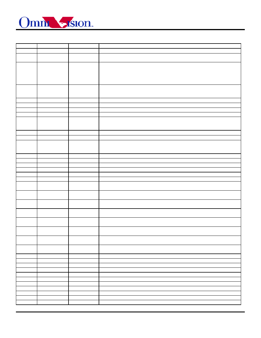
Figure 1. OV6630/OV6130 Pin Assignments
Array Element(CIF)
(QCIF)
352x288
(176x144)
Pixel Size
9
�m x 8.2�m
Image Area
3.1mm x 2.5mm
Max Frames/Sec
Up to 60 FPS
Electronics
Exposure
Up to 500:1 (for selected
FPS)
Scan Mode
Progressive
Gamma Correction
0.45/0.55/1.0
Min. Illumination
(3000K)
OV6630 - < 3lux @ f1.2
OV6130 - < 0.5lux @ f1.2
S/N Ration
> 48 dB
(AGC off, Gamma=1)
FPN
< 0.03% V
PP
Dark Current
< 0.2nA/cm
2
Dynamic Range
> 72 dB
Power Supply
3.0
-3.6VDC
5VDC/3.3VDC (DIO)
Power
Requirements
< 20mA active
< 10
�A Standby
Package
48 pin LCC
Note: Outputs UV0-UV7 are not available on the OV6130. The inputs associated
with these respective pins are still functional.
OmniVision Technologies, Inc. 930 Thompson Place Sunnyvale, CA 94086 U.S.A.
Tel: (408) 733-3030 Fax: (408) 733-3061
e-mail:
info@ovt.com
Website: http://www.ovt.com
Version 1.0, March 4, 2000
SINGLE IC CMOS COLOR AND B/W DIGITAL CAMERAS
Table 1. Pin Description
Pin No.
Name
Pin Type
Function/Description
01 SVDD
V
IN
Array power (+3.3VDC)
02 RESET
Function
(Default=0)
Chip reset, active high
03 AGCEN
Function
(Default=0)
Automatic Gain Control (AGC) selection
"0" � Disable AGC
"1" � Enable AGC
Note: This function is disabled when OV6630/OV6130 sensor is configured in SCCB
mode.
04 FREX
Function
(Default=0)
Frame exposure control
"0" � Disable frame exposure control
"1" � Enable frame exposure control
05 HVDD
V
REF
(4V)
Charge pump voltage. Connect to ground through 10
�F capacitor.
06 ASUB
V
IN
Analog substrate voltage.
07 AGND
V
IN
Analog
ground
08 AVDD
V
IN
Analog power supply (+3.3VDC)
09 PWDN
Function
(Default=0)
Power down mode selection.
"0" � Normal mode.
"1" � Power down mode.
10 VRCAP1
V
REF
(1.5V)
Array reference. Connect to ground through 0.1
�F capacitor.
11 V
C
CHG V
REF
(2.7V)
Internal voltage reference. Connect to ground through 1
�F capacitor.
12 SCCBB
Function
(Default=0)
SCCB enable selection.
"0" � Enable SCCB
"1" � Enable auto-control mode
13
VTO
O
Luminance composite signal output (black/white in PAL standard).
14 ADVDD
V
IN
Analog power supply (+3.3VDC)
15 ADGND
V
IN
Analog signal ground
16
VSYNC/CSYS
I/O
Vertical sync output. At power up, read as CSYS.
17
FODD/CLK
I/O
Field ID FODD output or main clock output
18
HREF/VSFRAM I/O
HREF output. At power up, read as VSFRAM
19
*
UV7/B8
I/O
Bit 7 of U video component output. At power up, sampled as B8.
* Note: Output UV7 is not available on the OV6130 sensor.
20
*
UV6/ABKEN
I/O
Bit 6 of U video component output. At power up, sampled as ABKEN.
* Note: Output UV6 is not available on the OV6130 sensor.
21
*
UV5/MIR
I/O
Bit 5 of U video component output. At power up, sampled as MIR.
* Note: Output UV5 is not available on the OV6130 sensor.
22
*
UV4
I/O
Bit 4 of U video component output.
* Note: Output UV4 is not available on the OV6130 sensor.
23
*
UV3
I/O
Bit 3 of U video component output.
* Note: Output UV3 is not available on the OV6130 sensor.
24
*
UV2/QCIF
I/O
Bit 2 of U video component output. At power up, sampled as QCIF.
* Note: Output UV2 is not available on the OV6130 sensor.
25
*
UV1/CC656
I/O
Bit 1 of U video component output. At power up, sampled as CC656.
* Note: Output UV1 is not available on the OV6130 sensor.
26
*
UV0/GAMMA
I/O
Bit 0 of U video component output. At power up, sampled as GAMMA.
* Note: Output UV0 is not available on the OV6130 sensor.
27
XCLK1
I
Crystal clock input
28
XCLK2
O
Crystal clock output
29 DVDD
V
IN
Digital power supply (+3.3VDC)
30 DGND
V
IN
Digital
ground
31 DOGND
V
IN
Digital interface output buffer ground
32 DOVDD
V
IN
Digital interface output buffer power supply (+3.3VDC or 5VDC)
33
PCLK/PWDB
I/O
PCLK output. At power up sampled as PWDB.
34
Y7/CS0
I/O
Bit 7 of Y video component output. At power up, sampled as CS0.
35
Y6/CS2
I/O
Bit 6 of Y video component output. At power up, sampled as CS2.
36
Y5/SHARP
I/O
Bit 5 of Y video component output. At power up, sampled as SHAPR.
37
Y4/CS1
I/O
Bit 4 of Y video component output. At power up, sampled as CS1.
March 4, 2000
Version 1.0
2
SINGLE IC CMOS COLOR AND B/W DIGITAL CAMERAS
38
Y3/RGB
I/O
Bit 3 of Y video component output. At power up, sampled as RGB.
39
Y2/G2X
I/O
Bit 2 of Y video component output. At power up, sampled as G2X.
40
Y1
I/O
Bit 1 of Y video component output.
41
Y0/CBAR
I/O
Bit 0 of Y video component output. At power up, sampled as CBAR.
42 CHSYNC/BW
I/O
CHSYNC
output.
At power up, sampled as BW.
43 DEGND
V
IN
Decoder
ground.
44 DEVDD
V
IN
Decoder power supply (+3.3VDC)
45
SIO-1
I
SCCB serial interface clock input.
46
SIO-0
I/O
SCCB serial interface data input and output.
47 MULT
Function
(Default=0)
SCCB slave selection
"0" � Select single slave ID.
"1" � Enable multiple (8) slaves.
48 SGND
V
IN
Array
ground
1 Function
Description
(Note: References to color features do not apply to the OV6130 B&W Digital Image Sensor.)
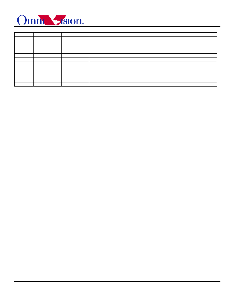
1.1 Overview
Referring to Figure 2 below, the OV6630 sensor includes a 356 x 292
resolution image array, an analog signal processor, dual 8-bit A/D
converters, analog video multiplexer, digital data formatter, video
port, SCCB interface, registers, and digital controls that include
timing block, exposure control, black level control, and white balance.
The OV6630/OV6130 sensor is a � inch CMOS imaging device. The
sensor contains approximately 101,376 pixels (352x288). Its design is
based on a field integration read-out system with line-by-line transfer
and an electronic shutter with a synchronous pixel read out scheme.
The color filter of the sensor consists of a primary color RG/GB array
arranged in line-alternating fashion.
March 4, 2000
Version 1.0
3

SINGLE IC CMOS COLOR AND B/W DIGITAL CAMERAS
WB
Detect
Column Sense Amp
B
Cr
R
PR
OG
Exposure
Control
1/2
AG
CEN
Analog
Prcssing
A/D
MUX
SC
CBB
Cb
Y[7:0]
Exposure
Detect
UV[7:0]
Fo
rmat
ter
SI
O-1
GA
MMA
Ro
w S
ele
ct
(356x292)
Image Array
WB
Control
A/D
SI
O-0
XC
LK1
AW
B
Video Timig
Generator
Vi
deo por
t
Y
AW
BTH
/
AW
BTM
SCCB
Interface
VTO
G
Registes
MUX
HR
EF
PC
LK
VS
YNC
FO
DD
CH
SYN
C
MI
R
Figure 2. OV6630/OV6130 CMOS Image Sensor Block Diagram
1.2 Analog Processor Circuits
1.2.1 Overview
The image is captured by the 356 x 292 pixel image array and routed
to the analog processing section where the majority of signal
processing occurs. This block contains the circuitry that performs
color separation, color correction, automatic gain control (AGC),
gamma correction, color balance, black level calibration, "knee"
smoothing, aperture correction, controls for picture luminance and
chrominance, and anti-alias filtering. The analog video signals are
based on the following formula:
Y = 0.59G + 0.31R + 0.11B
U = R � Y
V = B � Y
Where R,G,B are the equivalent color components in each
pixel.
YCrCb format is also supported, based on the formula below:
Y = 0.59G + 0.31R + 0.11B
Cr = 0.713 (R � Y)
Cb = 0.564 (B � Y)
The YCrCb/RGB data signal from the analog processing section is
fed to two on-chip 8-bit analog-to-digital (A/D) converters: one for
the Y/RG channel and one shared by the CrCb/BG channels. The
converted data stream is further conditioned in the digital formatter.
The processed signal is delivered to the digital video port through the
video multiplexer which routes the user-selected 16-, 8-, or 4-bit
video data to the correct output pins.
The on-chip 8-bit A/D operates up to 9 MHz, and fully synchronous
to the pixel rate. Actual conversion rate is related to the frame rate.
A/D black-level calibration circuitry ensures:
The black level of Y/RGB is normalized to a value of 16
The peak white level is limited to 240
CrCb black level is 128
CrCb Peak/bottom is 240/16
RGB raw data output range is 16/240
(Note: Values 0 and 255 are reserved for sync flag)
March 4, 2000
Version 1.0
4

SINGLE IC CMOS COLOR AND B/W DIGITAL CAMERAS
1.2.2 Image
Processing
The algorithm used for the electronic exposure control is based on the
brightness of the full image. The exposure is optimized for a "normal"
scene that assumes the subject is well lit relative to the background. In
situations where the image is not well lit, the automatic exposure
control (AEC) white/black ratio may be adjusted to suit the needs of
the application.
Additional on-chip functions include
AGC that provides a gain boost of up to 24dB
White balance control that enables setting of proper color
temperature and can be programmed for automatic or manual
operation.
Separate saturation, brightness, contrast, and sharpness
adjustments allow for further fine-tuning of the picture quality
and characteristics.
The OV6630 image sensor also provides control over the White
Balance ratio for increasing/decreasing the image field Red/Blue
component ratio. The sensor provides a default setting that may be
sufficient for many applications.
1.2.3 Windowing
The windowing feature of the OV6630/OV6130 image sensors allows
user-definable window sizing as required by the application. Window
size setting (in pixels) ranges from 2 x 2 to 356 x 292, and can be
positioned anywhere inside the 356 x 292 boundary. Note that
modifying window size and/or position does not change frame or data
rate. The OV6630/OV6130 imager alters the assertion of the HREF
signal to be consistent with the programmed horizontal and vertical
region. The default output window is 352 x 288.
1.2.4
Zoom Video Port (ZV)
The OV6630/OV6130 image sensor includes a Zoom Video (ZV)
function that supports standard ZV Port interface timing. Signals
available include VSYNC, CHSYNC, PCLK and 16-bit data bus:
Y[7:0] and UV[7:0]. The rising edge of PCLK clocks data into the ZV
port. See Figure 3. Zoom Video Port Timing below.
March 4, 2000
Version 1.0
5